EP0385643A2 - Quantum-Well-Laser mit vertikalem Resonator - Google Patents
Quantum-Well-Laser mit vertikalem Resonator Download PDFInfo
- Publication number
- EP0385643A2 EP0385643A2 EP90301850A EP90301850A EP0385643A2 EP 0385643 A2 EP0385643 A2 EP 0385643A2 EP 90301850 A EP90301850 A EP 90301850A EP 90301850 A EP90301850 A EP 90301850A EP 0385643 A2 EP0385643 A2 EP 0385643A2
- Authority
- EP
- European Patent Office
- Prior art keywords
- laser
- lasing
- mirror
- well
- reflectance
- Prior art date
- Legal status (The legal status is an assumption and is not a legal conclusion. Google has not performed a legal analysis and makes no representation as to the accuracy of the status listed.)
- Ceased
Links
Images



Classifications
-
- H—ELECTRICITY
- H01—ELECTRIC ELEMENTS
- H01S—DEVICES USING THE PROCESS OF LIGHT AMPLIFICATION BY STIMULATED EMISSION OF RADIATION [LASER] TO AMPLIFY OR GENERATE LIGHT; DEVICES USING STIMULATED EMISSION OF ELECTROMAGNETIC RADIATION IN WAVE RANGES OTHER THAN OPTICAL
- H01S5/00—Semiconductor lasers
- H01S5/30—Structure or shape of the active region; Materials used for the active region
-
- H—ELECTRICITY
- H01—ELECTRIC ELEMENTS
- H01S—DEVICES USING THE PROCESS OF LIGHT AMPLIFICATION BY STIMULATED EMISSION OF RADIATION [LASER] TO AMPLIFY OR GENERATE LIGHT; DEVICES USING STIMULATED EMISSION OF ELECTROMAGNETIC RADIATION IN WAVE RANGES OTHER THAN OPTICAL
- H01S5/00—Semiconductor lasers
- H01S5/04—Processes or apparatus for excitation, e.g. pumping, e.g. by electron beams
- H01S5/041—Optical pumping
-
- H—ELECTRICITY
- H01—ELECTRIC ELEMENTS
- H01S—DEVICES USING THE PROCESS OF LIGHT AMPLIFICATION BY STIMULATED EMISSION OF RADIATION [LASER] TO AMPLIFY OR GENERATE LIGHT; DEVICES USING STIMULATED EMISSION OF ELECTROMAGNETIC RADIATION IN WAVE RANGES OTHER THAN OPTICAL
- H01S5/00—Semiconductor lasers
- H01S5/10—Construction or shape of the optical resonator, e.g. extended or external cavity, coupled cavities, bent-guide, varying width, thickness or composition of the active region
- H01S5/18—Surface-emitting [SE] lasers, e.g. having both horizontal and vertical cavities
- H01S5/183—Surface-emitting [SE] lasers, e.g. having both horizontal and vertical cavities having only vertical cavities, e.g. vertical cavity surface-emitting lasers [VCSEL]
-
- H—ELECTRICITY
- H01—ELECTRIC ELEMENTS
- H01S—DEVICES USING THE PROCESS OF LIGHT AMPLIFICATION BY STIMULATED EMISSION OF RADIATION [LASER] TO AMPLIFY OR GENERATE LIGHT; DEVICES USING STIMULATED EMISSION OF ELECTROMAGNETIC RADIATION IN WAVE RANGES OTHER THAN OPTICAL
- H01S5/00—Semiconductor lasers
- H01S5/40—Arrangement of two or more semiconductor lasers, not provided for in groups H01S5/02 - H01S5/30
- H01S5/42—Arrays of surface emitting lasers
- H01S5/423—Arrays of surface emitting lasers having a vertical cavity
-
- H—ELECTRICITY
- H01—ELECTRIC ELEMENTS
- H01S—DEVICES USING THE PROCESS OF LIGHT AMPLIFICATION BY STIMULATED EMISSION OF RADIATION [LASER] TO AMPLIFY OR GENERATE LIGHT; DEVICES USING STIMULATED EMISSION OF ELECTROMAGNETIC RADIATION IN WAVE RANGES OTHER THAN OPTICAL
- H01S5/00—Semiconductor lasers
- H01S5/02—Structural details or components not essential to laser action
- H01S5/026—Monolithically integrated components, e.g. waveguides, monitoring photo-detectors, drivers
- H01S5/0261—Non-optical elements, e.g. laser driver components, heaters
-
- H—ELECTRICITY
- H01—ELECTRIC ELEMENTS
- H01S—DEVICES USING THE PROCESS OF LIGHT AMPLIFICATION BY STIMULATED EMISSION OF RADIATION [LASER] TO AMPLIFY OR GENERATE LIGHT; DEVICES USING STIMULATED EMISSION OF ELECTROMAGNETIC RADIATION IN WAVE RANGES OTHER THAN OPTICAL
- H01S5/00—Semiconductor lasers
- H01S5/02—Structural details or components not essential to laser action
- H01S5/026—Monolithically integrated components, e.g. waveguides, monitoring photo-detectors, drivers
- H01S5/0262—Photo-diodes, e.g. transceiver devices, bidirectional devices
-
- H—ELECTRICITY
- H01—ELECTRIC ELEMENTS
- H01S—DEVICES USING THE PROCESS OF LIGHT AMPLIFICATION BY STIMULATED EMISSION OF RADIATION [LASER] TO AMPLIFY OR GENERATE LIGHT; DEVICES USING STIMULATED EMISSION OF ELECTROMAGNETIC RADIATION IN WAVE RANGES OTHER THAN OPTICAL
- H01S5/00—Semiconductor lasers
- H01S5/02—Structural details or components not essential to laser action
- H01S5/026—Monolithically integrated components, e.g. waveguides, monitoring photo-detectors, drivers
- H01S5/0262—Photo-diodes, e.g. transceiver devices, bidirectional devices
- H01S5/0264—Photo-diodes, e.g. transceiver devices, bidirectional devices for monitoring the laser-output
-
- H—ELECTRICITY
- H01—ELECTRIC ELEMENTS
- H01S—DEVICES USING THE PROCESS OF LIGHT AMPLIFICATION BY STIMULATED EMISSION OF RADIATION [LASER] TO AMPLIFY OR GENERATE LIGHT; DEVICES USING STIMULATED EMISSION OF ELECTROMAGNETIC RADIATION IN WAVE RANGES OTHER THAN OPTICAL
- H01S5/00—Semiconductor lasers
- H01S5/10—Construction or shape of the optical resonator, e.g. extended or external cavity, coupled cavities, bent-guide, varying width, thickness or composition of the active region
- H01S5/18—Surface-emitting [SE] lasers, e.g. having both horizontal and vertical cavities
- H01S5/183—Surface-emitting [SE] lasers, e.g. having both horizontal and vertical cavities having only vertical cavities, e.g. vertical cavity surface-emitting lasers [VCSEL]
- H01S5/18305—Surface-emitting [SE] lasers, e.g. having both horizontal and vertical cavities having only vertical cavities, e.g. vertical cavity surface-emitting lasers [VCSEL] with emission through the substrate, i.e. bottom emission
Definitions
- OEIC's - Contemplated uses for integrated lasers - largely represented by OEIC's - include integration with the driving electronics itself as well as inclusion of elements to provide for interaction both within photonic parts of the circuit and between photonic and electronic parts. Examples of purely photonic interaction include laser-to-detector. There are many examples of the second category.
- OEIC's As identified in recent literature include imaging, image processing and optical gas detection.
- the quarter-wave mirror structures in the described experiment consisted of eight layers each of the two materials. Excellent properties observed showed a 54 ⁇ centered transmission band at a wavelength of 0.956 nm.
- the authors report certain properties from which it is possible to calculate absorption/scattering losses of their structure. Properties reported include a peak transmittance of 45%, as well as their calculated “ideal structure" transmittance of 68%.
- the initially vertically directed emitted beam This is of value, for example, in chip-to-chip communication and in certain other instances in which laser output is to be coupled with external circuitry.
- the vertical structure also offers low threshold-related advantages for use involving communication within the chip (or under other circumstances in which coupling is in a direction parallel to the major substrate plane).
- the initially non-parallel beam as emitted by the laser may be redirected, for example, by use of a mirror or prism external to the cavity itself.
- Such mirrors, likely DFB's, of the same nature discussed in conjunction with the cavity itself could be fabricated as part of an integrated circuit.
- the Gourley et al article is representative of the most advanced state of the art at least in terms of DFB mirror cavities. It serves as basis for explaining the general view that a small number of quantum wells is inadequate for lasing.
- a Fabray-Perot etalon has a net maximal transmission of T2/(T+A)2, a relationship well-known to workers in relevant fields and found in many textbooks on optics.
- T is the transmittance of a single mirror of the Fabray-Perot etalon and A is the fraction of energy absorbed by the same mirror. Energy not transmitted or absorbed is reflected.
- cavity efficiency is dependent upon mirror efficiency which, in turn, varies ⁇ as the reciprocal of the difference in refractive index between the two successive layered mirror materials ( ⁇ n). Since, in general, refractive index for suitable mirror materials varies less for increasing wavelength, ⁇ n values are typically less so that a greater number of layers is generally required for the necessary cumulative reflectivities.
- the invention derives from the conclusion that distributed feedback mirrors have better attainable characteristics than previously believed.
- the inventive finding of unexpectedly good reflectivity v loss characteristics has extremely significant characteristics in terms of all Q uantum W ell V ertical C avity L asers - electrically pumped as well as optically pumped.
- Implications of the invention are significant in terms of discrete devices since more effective cavitation permits lasing for lower threshold - for less efficient active materialsas ell as for lesser numbers of quantum wells - as few as two, or even one. Most significantly, however, implications of the invention are in terms of integration. The inventive finding, in giving rise to lower threshold, results in lower power dissipation. Specific structures of the invention - primarily laser-including integrated circuits are possible because of low needed heat dissipation - e.g. in terms of lower permitted device threshold power - as corresponding with small numbers of QW's - two or even one ( S ingle Q uantum W ell structures). Inventive devices are described also in terms of the larger fraction of free wafer surface that may be used for active lasing which translates into permitted integration density, and in turn, generally into permitted design rules.
- While structures of the invention are naturally utilized for chip-to-chip (or generally to offchip) communication, other structures provide for out-of-plane emission beams, e.g. by redirection with mirrors or prisms, to enable within-chip communication.
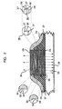
- FIG. 1 depicts an optically pumped SQW structure consisting of lens 10 for directing incoming radiation 11 which first passes through substrate 12 and thereafter through DFB mirror 13 composed of alternating pairs of high and low refractive index material 14 and 15, respectively. Radiation thereafter is introduced into QW structure 16 consisting of one or two quantum wells 16′ embedded in barrier material 17. The structure is completed by mirror 19 which similar to 13 is made up of alternating layers of high and low refractive index material 14 and 15. In the arrangement shown, the emitted lasing beam emerges vertically upward as shown by the arrows.
- FIG. 2 The structure of FIG. 2 is similar to that of FIG. 1 but provides for electrical rather than optical pumping via electrodes 23 and 24.
- the structure 25 is similar to that of FIG. 1 and again consists of QW structure 26 made up of well/s 26 ′embedded in barrier material 27. Cavitation as in FIG. 1 is the consequence of DFB mirrors 29 and 30 each again consisting of quarter wavelength layers, in this instance of alternating refractive index 31, 32 and 33, 34 which may be the same for both mirrors).
- mirrors 29 and 30 are doped, one with m-type, the other with p-type dopant to produce the pn junction responsible for generation of carriers in the usual manner for electrically pumped semiconductor lasers.
- Current pumping produced by means of electrical source not shown, results in current flow between electrodes 23 and 24 in the form of current represented by arrows 35.
- the emerging laser beam, again upwardly directed, is represented by arrows 36.
- Region 37 is composed of dielectric material.
- FIG. 3 The structure of FIG. 3 is functionally similar to FIG. 2 and differs primarily in providing for a face electrode 38 of sufficient reflectivity so that emission is in the form of a downward-directed beam 39 shown in the form of arrows emerging from the underside of substrate 40. Otherwise, the structure is as shown in FIG. 2, being composed of active quantum well structure 41, either one or two wells comprising active material 41 ′ embedded in barrier material 42. Mirrors 44 and 45, composed of alternating high and low refractive index layers 46, 47 and 48, 49, respectively, complete the structure optically. Electrical pumping from means not shown, is across electrodes 38 and 50.
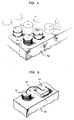
- FIG. 4 depicts an array of lasers 51 which may be of the detailed design shown in any of FIGS. 1 through 3.
- lasers 51 are supported on a substrate, in this instance 52, upon which an in at least some instances, they were grown, for example, by M olecular B eam E pitaxy.
- Lasers depicted in this figure as well as in FIGS. 5 and 6 are exaggerated in dimension in the lasing direction. In general, they are only a few microns in height.
- FIG. 5 shows a portion of an OEIC.
- the portion shown consists simply of a laser 53 together with drive electronics 54 both on common substrate 55.
- the arrangement is schematically shown as connected via lead 56 with the electrical circuit being completed by a common substrate lead.
- FIG. 6 is representative of an important aspect of the invention and shows an integrated circuit including both a laser 57 driven via lead 58 and the conducting surface of substrate 59 by driving circuitry 60.
- the structure shown provides for an optic-to-electronic detector 61 which upon detecting light beam 62 as received from incoming optical fiber 63 converts it to an electrical impulse introduced into the driving ciruit 60 by means of lead 64 and the surface of substrate 59.
- the integrated circuit shown provides for within-chip communication by redirecting vertically emitting beam 64 by means of prisms 65 and 66 to result in beam 64 being made incident on detector 67.
- a first requirement for optimum structures in accordance with the invention is sufficient crystalline perfection - sufficient absence of dislocations - to permit operation as discussed later. Whereas it would be desirable that all materials utilized be of identical crystalline lattice constants in the appropriate directions, other (device-significant) considerations sometimes dictate choice of materials that are not precisely matched. It is well known in the art that sufficient freedome of dislocations ("quasimorphic" structures) are attainable with materials of differing lattice constants. Appropriate growth conditions which depend, inter alia, on the degree of difference of the constants, on growth conditions, on total thickness grown, etc. are discussed, for example, by J. W. Matthews and A. E. Blakeslee, J. Cryst. Growth , Vol. 27, p. 1187 (1974).
- Active material of which the quantum well is composed must have a direct energy bandgap suitable for the desired radiation wavelength, and must otherwise be suitable for lasing.
- the active material is embedded in barrier material (is sandwiched between two barrier layers).
- Barrier material also a direct bandgap material, has a higher energy gap and serves the function of confinement of carriers within the active material.
- Mirror structures are composed of alternating layers of material of differing refractive index.
- the difference in index ⁇ n should be as large as possible since the required number of layers for a desired reflectance is smaller for large ⁇ n.
- otherwise suitable mirror materials of a ⁇ n of at least 0.2 (expressed as the difference between the two refractive indices expressed in usual dimensionless quantities relative to vacuum) may be used.
- electrodes are provided with apertures for emitting beams so that the requirements are uncomplicated by laser function, e.g., pertains to electrical and fabrication properties such as e.g. conductivity, adherence, stability, etc.
- the electrode material is applied as an extremely thin layer.
- Electrically pumped structures require pn junctions - require both p and n type material.
- the two embracing mirror assemblies are oppositely doped, one p type the other n type, again in accordance with well-understood technology, e.g. as developed to an advanced state relative to edge-emitting quantum well structures.
- inventive teaching relies on the high level of development to which the relevant laser art has been developed.
- active materials - appropriate direct bandgap materials - are the compound semiconductors such as selected materials of the III-V, the II-VI, and the ternaries, quaternaries as well as more complex compositions. In common with reported laser work, such active materials may be true compounds - sometimes partially substituted, or functioning may be dependent upon inclusion of critical dopants.
- inventive teaching does not depend on designation of appropriate lasing compositions. Illustrative active materials suitable for the inventive structures, as well as for prior art structures, are listed.
- desired lasing wavelength while necessarily permitted by the bandgap of the active material, depends to some extent on other considerations including well-dimension positioning within the cavity, nature of the barrier material, etc.
- Appropriate active material - barrier material couples together with typical lasing wavelengths are listed: GaAs/AlGaAs - 0.85 ⁇ m; In 0.53 Ga 0.47 As/InP- 1.55 ⁇ m; In 0.2 Ga 0.8 As/GaAs-1 ⁇ m.
- Very thin layers are more likely to have more consequential surface roughness (properly considered as a fraction of total thickness) while thicknesses very much larger than 100-120Angstrom unit result in bulk properties.
- a useful reference authored by Arakawa and Yariv is IEEE Journal of Quantum Electronics Vol. 21, p. 1666, 1985.
- barrier thickness As a general premise, precise dimensions of the barrier material are non-critical. Experiments suggest that so long as there is a continuous coating of barrier of a few atoms thickness, the primary function of carrier confinement is satisfied. In practice, however, it is convenient to adjust barrier thickness so that it, together with the active material, defines the "spacer" dimension to attain most effective resonant quality. This gives rise to inclusion of at least one barrier layer thickness which is at least as large or larger than that of an individual mirror layer.
- DFB mirror structures are, again, well known. (See J. P. van der Ziel and M. Ilegem, Appl. Opt. 14, 2627, 1975.)
- the basic requirement is for alternating layers of relatively high and low refractive index with layer thicknesses such as to permit resonance - most effective structures utilized quarter wavelength thicknesses. Assuming other desired characteristics, such a chemical stability, low absorption loss, etc. are satisfied, optimization is in the direction of largest available ⁇ n as discussed above.
- the invention depends upon the finding that "ideal" structures - in fact practically attainable structures - are characterized by sufficiently good properties to permit lasing of single or double quantum well structures.
- cavity structures are characterized by mirrors of perhaps 22 or preferably (at least from the operational standpoint) 24 or more layer pairs.
- Certain structures of the invention make use of unbalanced mirror reflectances. When device requirement is for a single output direction, it may be achieved by increasing reflectance to a greater value at the non-emitting side. One manner for accomplishing this is to provide a greater number of layers at the non-emitting side of the cavity. The same imbalance serves a fundamental purpose: since each additional mirror layer reduces transmission while increasing reflectance, and assuming non-critical added absorption/scattering loss, the desire for higher reflectance, and therefore accommodation of lower threshold, is satisfied without penalty by increasing the number of layers on the non-transmitting side of the cavity.
- the maximum number of layers is, in any event, no greater than that corresponding with the crossover at which added loss per added layer exceeds reduced pump transmission loss per added layer.
- mirror structures may have fewer layers than this maximum since "incalculable" losses (e.g. absorption, scattering) give rise to an effective crossover for a smaller structure and/or because of fabrication cost/complexity.
- an important aspect of the invention - cavity structures depending upon observed excellence of reflectance v loss characteristics - is properly stated as permitting attainment of needed cavitation to accomplish lasing for relatively low gain structures (single or duplex QWVCL's) including those in which the improvement is ascribed more to one mirror structure than to the other.
- a single quantum well structure of the design shown in FIG. 1, utilizes an 80 ⁇ thick well of area about 400 square micrometers, composed of In 0.2 Ga 0.8 As sandwiched between 1290 ⁇ barrier layers of GaAs.
- the upper mirror structure is composed of 24 pairs of quarter-wavelength thick layers of GaAs and AlAs.
- GaAs has the greater index ( ⁇ 3.5), AlAs has the smaller ( ⁇ 2.9).
- Quarter wavelength for GaAs is 670 ⁇ while for AlAs it is 80 ⁇ .
- the GaAs substrate - of non-critical dimension - is 500 ⁇ m.
- MBE epitaxial layer growth is on a substrate of crystallographic orientation (100).
- the structure is pumped by a synchronously pumped dye laser emitting at a wavelength of 860nm.
- the output laser beam as emitted through the substrate, has a center wavelength of 980nm. Lasing threshold is 7 microwatts per square micrometer.
- Example 1 is repeated, however, substituting a pump wavelength of 880 nm. At this wavelength only the active material - the In-containing material - absorbs. Threshold is about the same and it is not apparent that either example is fundamentally preferable. The observation is ascribed to the surmise that the greater absorption by use of the 860 nm pump does not result in 100% carrier transfer to the active region.
- quantum well structures which for this purpose may include barrier material and even some part of adjacent mirror
- Active structures support standing waves. Effective amplification of resonating energy requires placement of the quantum well as nearly coincident with an energy peak of the standing wave as possible.
- the finite band of laser wavelengths available - those within the band permitted by the active material - permits and, in fact results, in accommodation so that the quantum well is indeed coincident with a peak.
- More complex structures - those containing two quantum wells may or may not accommodate depending upon other structural considerations - for example, thickness of barrier material between the wells.
- design rule In the terminology generally used in integration, e.g. in l arge s cale i ntegration, the term "design rule" has reference to minimum feature size (as well as to other considerations such as spacing between features, etc.). In these terms circuits may be described as of design rules corresponding with the dimensions listed above.
Landscapes
- Physics & Mathematics (AREA)
- Condensed Matter Physics & Semiconductors (AREA)
- General Physics & Mathematics (AREA)
- Electromagnetism (AREA)
- Optics & Photonics (AREA)
- Semiconductor Lasers (AREA)
- Physical Deposition Of Substances That Are Components Of Semiconductor Devices (AREA)
Applications Claiming Priority (2)
| Application Number | Priority Date | Filing Date | Title |
|---|---|---|---|
| US07/317,699 US4999842A (en) | 1989-03-01 | 1989-03-01 | Quantum well vertical cavity laser |
| US317699 | 1989-03-01 |
Publications (2)
| Publication Number | Publication Date |
|---|---|
| EP0385643A2 true EP0385643A2 (de) | 1990-09-05 |
| EP0385643A3 EP0385643A3 (de) | 1991-07-17 |
Family
ID=23234876
Family Applications (1)
| Application Number | Title | Priority Date | Filing Date |
|---|---|---|---|
| EP19900301850 Ceased EP0385643A3 (de) | 1989-03-01 | 1990-02-21 | Quantum-Well-Laser mit vertikalem Resonator |
Country Status (5)
| Country | Link |
|---|---|
| US (1) | US4999842A (de) |
| EP (1) | EP0385643A3 (de) |
| JP (1) | JP2572143B2 (de) |
| KR (1) | KR940004425B1 (de) |
| CA (1) | CA2008904C (de) |
Cited By (3)
| Publication number | Priority date | Publication date | Assignee | Title |
|---|---|---|---|---|
| EP0562768A1 (de) * | 1992-03-25 | 1993-09-29 | AT&T Corp. | Oberflächenemittierender Halbleiterlaser mit reduzierter Schwellspannung und erhöhter optischer Ausgangsleistung |
| EP0395315B1 (de) * | 1989-04-26 | 1994-01-19 | AT&T Corp. | Elektrisch gepumpter Laser mit senkrechtem Resonator |
| GB2307791A (en) * | 1995-11-30 | 1997-06-04 | Hewlett Packard Co | Vertical cavity surface emitting lasers |
Families Citing this family (88)
| Publication number | Priority date | Publication date | Assignee | Title |
|---|---|---|---|---|
| US5132750A (en) * | 1989-11-22 | 1992-07-21 | Daido Tokushuko Kabushiki Kaisha | Light-emitting diode having light reflecting layer |
| US5289018A (en) * | 1990-08-14 | 1994-02-22 | Canon Kabushiki Kaisha | Light emitting device utilizing cavity quantum electrodynamics |
| US5412229A (en) * | 1990-08-31 | 1995-05-02 | Sumitomo Electric Industries, Ltd. | Semiconductor light detecting device making use of a photodiode chip |
| US5253262A (en) * | 1990-10-31 | 1993-10-12 | Kabushiki Kaisha Toshiba | Semiconductor laser device with multi-directional reflector arranged therein |
| EP0483868B1 (de) * | 1990-11-02 | 1997-01-22 | Norikatsu Yamauchi | Halbleitervorrichtung mit reflektierender Schicht |
| US5146465A (en) * | 1991-02-01 | 1992-09-08 | Apa Optics, Inc. | Aluminum gallium nitride laser |
| US5182670A (en) * | 1991-08-30 | 1993-01-26 | Apa Optics, Inc. | Narrow band algan filter |
| US5206872A (en) * | 1991-11-01 | 1993-04-27 | At&T Bell Laboratories | Surface emitting laser |
| US5258990A (en) * | 1991-11-07 | 1993-11-02 | The United States Of America As Represented By The Secretary Of The United States Department Of Energy | Visible light surface emitting semiconductor laser |
| DE69217344T2 (de) * | 1991-12-16 | 1997-08-21 | Ibm | Abstimmbarer Laser mit gekoppelter Quantumwell-Struktur |
| US5266794A (en) * | 1992-01-21 | 1993-11-30 | Bandgap Technology Corporation | Vertical-cavity surface emitting laser optical interconnect technology |
| US5245622A (en) * | 1992-05-07 | 1993-09-14 | Bandgap Technology Corporation | Vertical-cavity surface-emitting lasers with intra-cavity structures |
| US5278435A (en) * | 1992-06-08 | 1994-01-11 | Apa Optics, Inc. | High responsivity ultraviolet gallium nitride detector |
| US5249195A (en) * | 1992-06-30 | 1993-09-28 | At&T Bell Laboratories | Erbium doped optical devices |
| US5264715A (en) * | 1992-07-06 | 1993-11-23 | Honeywell Inc. | Emitting with structures located at positions which prevent certain disadvantageous modes and enhance generation of light in advantageous modes |
| US5244749A (en) * | 1992-08-03 | 1993-09-14 | At&T Bell Laboratories | Article comprising an epitaxial multilayer mirror |
| US5483511A (en) * | 1993-02-17 | 1996-01-09 | Vixel Corporation | Multiple beam optical memory system with solid-state lasers |
| US5526182A (en) * | 1993-02-17 | 1996-06-11 | Vixel Corporation | Multiple beam optical memory system |
| US5675436A (en) * | 1995-04-05 | 1997-10-07 | Lucent Technologies Inc. | Optical image processor employing a nonlinear medium with active gain |
| US5513203A (en) * | 1995-04-05 | 1996-04-30 | At&T Corp. | Surface emitting laser having improved pumping efficiency |
| DE19523267A1 (de) * | 1995-06-27 | 1997-01-02 | Bosch Gmbh Robert | Lasermodul |
| US5694412A (en) * | 1996-04-08 | 1997-12-02 | He Holdings Inc. | Epitaxial visible-light-emitting devices with light extracted through the substrate and method of making same |
| US5960024A (en) | 1998-03-30 | 1999-09-28 | Bandwidth Unlimited, Inc. | Vertical optical cavities produced with selective area epitaxy |
| US6760357B1 (en) | 1998-04-14 | 2004-07-06 | Bandwidth9 | Vertical cavity apparatus with tunnel junction |
| US6535541B1 (en) | 1998-04-14 | 2003-03-18 | Bandwidth 9, Inc | Vertical cavity apparatus with tunnel junction |
| US6493371B1 (en) | 1998-04-14 | 2002-12-10 | Bandwidth9, Inc. | Vertical cavity apparatus with tunnel junction |
| US6493373B1 (en) | 1998-04-14 | 2002-12-10 | Bandwidth 9, Inc. | Vertical cavity apparatus with tunnel junction |
| US6487230B1 (en) | 1998-04-14 | 2002-11-26 | Bandwidth 9, Inc | Vertical cavity apparatus with tunnel junction |
| US5991326A (en) | 1998-04-14 | 1999-11-23 | Bandwidth9, Inc. | Lattice-relaxed verticle optical cavities |
| US6493372B1 (en) | 1998-04-14 | 2002-12-10 | Bandwidth 9, Inc. | Vertical cavity apparatus with tunnel junction |
| US6487231B1 (en) | 1998-04-14 | 2002-11-26 | Bandwidth 9, Inc. | Vertical cavity apparatus with tunnel junction |
| US6226425B1 (en) | 1999-02-24 | 2001-05-01 | Bandwidth9 | Flexible optical multiplexer |
| US6233263B1 (en) | 1999-06-04 | 2001-05-15 | Bandwidth9 | Monitoring and control assembly for wavelength stabilized optical system |
| US6275513B1 (en) | 1999-06-04 | 2001-08-14 | Bandwidth 9 | Hermetically sealed semiconductor laser device |
| US6392257B1 (en) | 2000-02-10 | 2002-05-21 | Motorola Inc. | Semiconductor structure, semiconductor device, communicating device, integrated circuit, and process for fabricating the same |
| US6693033B2 (en) | 2000-02-10 | 2004-02-17 | Motorola, Inc. | Method of removing an amorphous oxide from a monocrystalline surface |
| KR20030011083A (ko) | 2000-05-31 | 2003-02-06 | 모토로라 인코포레이티드 | 반도체 디바이스 및 이를 제조하기 위한 방법 |
| US6410941B1 (en) | 2000-06-30 | 2002-06-25 | Motorola, Inc. | Reconfigurable systems using hybrid integrated circuits with optical ports |
| US6427066B1 (en) | 2000-06-30 | 2002-07-30 | Motorola, Inc. | Apparatus and method for effecting communications among a plurality of remote stations |
| US6477285B1 (en) | 2000-06-30 | 2002-11-05 | Motorola, Inc. | Integrated circuits with optical signal propagation |
| US6501973B1 (en) | 2000-06-30 | 2002-12-31 | Motorola, Inc. | Apparatus and method for measuring selected physical condition of an animate subject |
| US6590236B1 (en) | 2000-07-24 | 2003-07-08 | Motorola, Inc. | Semiconductor structure for use with high-frequency signals |
| AU2001277001A1 (en) * | 2000-07-24 | 2002-02-05 | Motorola, Inc. | Heterojunction tunneling diodes and process for fabricating same |
| US6555946B1 (en) | 2000-07-24 | 2003-04-29 | Motorola, Inc. | Acoustic wave device and process for forming the same |
| US6482538B2 (en) | 2000-07-24 | 2002-11-19 | Motorola, Inc. | Microelectronic piezoelectric structure and method of forming the same |
| US6432546B1 (en) | 2000-07-24 | 2002-08-13 | Motorola, Inc. | Microelectronic piezoelectric structure and method of forming the same |
| US6493497B1 (en) | 2000-09-26 | 2002-12-10 | Motorola, Inc. | Electro-optic structure and process for fabricating same |
| US6638838B1 (en) | 2000-10-02 | 2003-10-28 | Motorola, Inc. | Semiconductor structure including a partially annealed layer and method of forming the same |
| US6583034B2 (en) | 2000-11-22 | 2003-06-24 | Motorola, Inc. | Semiconductor structure including a compliant substrate having a graded monocrystalline layer and methods for fabricating the structure and semiconductor devices including the structure |
| US6559471B2 (en) | 2000-12-08 | 2003-05-06 | Motorola, Inc. | Quantum well infrared photodetector and method for fabricating same |
| US6563118B2 (en) | 2000-12-08 | 2003-05-13 | Motorola, Inc. | Pyroelectric device on a monocrystalline semiconductor substrate and process for fabricating same |
| US20020096683A1 (en) * | 2001-01-19 | 2002-07-25 | Motorola, Inc. | Structure and method for fabricating GaN devices utilizing the formation of a compliant substrate |
| US6673646B2 (en) | 2001-02-28 | 2004-01-06 | Motorola, Inc. | Growth of compound semiconductor structures on patterned oxide films and process for fabricating same |
| US7046719B2 (en) | 2001-03-08 | 2006-05-16 | Motorola, Inc. | Soft handoff between cellular systems employing different encoding rates |
| WO2002082551A1 (en) | 2001-04-02 | 2002-10-17 | Motorola, Inc. | A semiconductor structure exhibiting reduced leakage current |
| US6709989B2 (en) | 2001-06-21 | 2004-03-23 | Motorola, Inc. | Method for fabricating a semiconductor structure including a metal oxide interface with silicon |
| US6992321B2 (en) | 2001-07-13 | 2006-01-31 | Motorola, Inc. | Structure and method for fabricating semiconductor structures and devices utilizing piezoelectric materials |
| US20030010992A1 (en) * | 2001-07-16 | 2003-01-16 | Motorola, Inc. | Semiconductor structure and method for implementing cross-point switch functionality |
| US6646293B2 (en) | 2001-07-18 | 2003-11-11 | Motorola, Inc. | Structure for fabricating high electron mobility transistors utilizing the formation of complaint substrates |
| US7019332B2 (en) | 2001-07-20 | 2006-03-28 | Freescale Semiconductor, Inc. | Fabrication of a wavelength locker within a semiconductor structure |
| US6693298B2 (en) | 2001-07-20 | 2004-02-17 | Motorola, Inc. | Structure and method for fabricating epitaxial semiconductor on insulator (SOI) structures and devices utilizing the formation of a compliant substrate for materials used to form same |
| US6472694B1 (en) | 2001-07-23 | 2002-10-29 | Motorola, Inc. | Microprocessor structure having a compound semiconductor layer |
| US6855992B2 (en) * | 2001-07-24 | 2005-02-15 | Motorola Inc. | Structure and method for fabricating configurable transistor devices utilizing the formation of a compliant substrate for materials used to form the same |
| US6667196B2 (en) | 2001-07-25 | 2003-12-23 | Motorola, Inc. | Method for real-time monitoring and controlling perovskite oxide film growth and semiconductor structure formed using the method |
| US6585424B2 (en) | 2001-07-25 | 2003-07-01 | Motorola, Inc. | Structure and method for fabricating an electro-rheological lens |
| US6594414B2 (en) | 2001-07-25 | 2003-07-15 | Motorola, Inc. | Structure and method of fabrication for an optical switch |
| US6462360B1 (en) | 2001-08-06 | 2002-10-08 | Motorola, Inc. | Integrated gallium arsenide communications systems |
| US6639249B2 (en) | 2001-08-06 | 2003-10-28 | Motorola, Inc. | Structure and method for fabrication for a solid-state lighting device |
| US6589856B2 (en) | 2001-08-06 | 2003-07-08 | Motorola, Inc. | Method and apparatus for controlling anti-phase domains in semiconductor structures and devices |
| US20030034491A1 (en) | 2001-08-14 | 2003-02-20 | Motorola, Inc. | Structure and method for fabricating semiconductor structures and devices for detecting an object |
| US6673667B2 (en) | 2001-08-15 | 2004-01-06 | Motorola, Inc. | Method for manufacturing a substantially integral monolithic apparatus including a plurality of semiconductor materials |
| US20030036217A1 (en) * | 2001-08-16 | 2003-02-20 | Motorola, Inc. | Microcavity semiconductor laser coupled to a waveguide |
| US20030071327A1 (en) * | 2001-10-17 | 2003-04-17 | Motorola, Inc. | Method and apparatus utilizing monocrystalline insulator |
| US6916717B2 (en) | 2002-05-03 | 2005-07-12 | Motorola, Inc. | Method for growing a monocrystalline oxide layer and for fabricating a semiconductor device on a monocrystalline substrate |
| US20040012037A1 (en) * | 2002-07-18 | 2004-01-22 | Motorola, Inc. | Hetero-integration of semiconductor materials on silicon |
| US20040070312A1 (en) * | 2002-10-10 | 2004-04-15 | Motorola, Inc. | Integrated circuit and process for fabricating the same |
| US20040069991A1 (en) * | 2002-10-10 | 2004-04-15 | Motorola, Inc. | Perovskite cuprate electronic device structure and process |
| US7169619B2 (en) | 2002-11-19 | 2007-01-30 | Freescale Semiconductor, Inc. | Method for fabricating semiconductor structures on vicinal substrates using a low temperature, low pressure, alkaline earth metal-rich process |
| US6885065B2 (en) | 2002-11-20 | 2005-04-26 | Freescale Semiconductor, Inc. | Ferromagnetic semiconductor structure and method for forming the same |
| US7112830B2 (en) * | 2002-11-25 | 2006-09-26 | Apa Enterprises, Inc. | Super lattice modification of overlying transistor |
| US7020374B2 (en) * | 2003-02-03 | 2006-03-28 | Freescale Semiconductor, Inc. | Optical waveguide structure and method for fabricating the same |
| US6965128B2 (en) * | 2003-02-03 | 2005-11-15 | Freescale Semiconductor, Inc. | Structure and method for fabricating semiconductor microresonator devices |
| US20040164315A1 (en) * | 2003-02-25 | 2004-08-26 | Motorola, Inc. | Structure and device including a tunneling piezoelectric switch and method of forming same |
| US7219018B2 (en) * | 2003-09-11 | 2007-05-15 | Franco Vitaliano | Quantum information processing elements and quantum information processing platforms using such elements |
| US7216038B2 (en) * | 2003-09-11 | 2007-05-08 | Franco Vitaliano | Quantum information processing elements and quantum information processing platforms using such elements |
| US7219017B2 (en) * | 2003-09-11 | 2007-05-15 | Franco Vitaliano | Quantum information processing elements and quantum information processing platforms using such elements |
| KR101240558B1 (ko) * | 2007-11-05 | 2013-03-06 | 삼성전자주식회사 | 광 연결 수단을 구비한 멀티칩 |
| JP6849371B2 (ja) * | 2015-10-08 | 2021-03-24 | 三星電子株式会社Samsung Electronics Co.,Ltd. | 側面発光レーザ光源、及びそれを含む三次元映像取得装置 |
Family Cites Families (8)
| Publication number | Priority date | Publication date | Assignee | Title |
|---|---|---|---|---|
| JPS59152684A (ja) * | 1983-02-21 | 1984-08-31 | Nec Corp | 量子井戸型面発光半導体レ−ザ |
| JPS6097684A (ja) * | 1983-10-31 | 1985-05-31 | Rohm Co Ltd | 半導体レーザ |
| JPS614291A (ja) * | 1984-06-19 | 1986-01-10 | Agency Of Ind Science & Technol | 面発光レ−ザ |
| JPS6179280A (ja) * | 1984-09-27 | 1986-04-22 | Agency Of Ind Science & Technol | 面発光型半導体レ−ザ装置及びその製造方法 |
| US4675876A (en) * | 1985-02-14 | 1987-06-23 | Northern Telecom Limited | Bragg distributed feedback surface emitting laser |
| JPH0419819Y2 (de) * | 1985-03-23 | 1992-05-06 | ||
| JPH01209776A (ja) * | 1987-02-20 | 1989-08-23 | Siemens Ag | レーザ送信器装置 |
| JPS63269594A (ja) * | 1987-04-27 | 1988-11-07 | Nec Corp | 面発光型双安定半導体レ−ザ |
-
1989
- 1989-03-01 US US07/317,699 patent/US4999842A/en not_active Expired - Lifetime
-
1990
- 1990-01-30 CA CA002008904A patent/CA2008904C/en not_active Expired - Fee Related
- 1990-02-21 EP EP19900301850 patent/EP0385643A3/de not_active Ceased
- 1990-02-28 KR KR1019900002599A patent/KR940004425B1/ko not_active Expired - Fee Related
- 1990-03-01 JP JP2047388A patent/JP2572143B2/ja not_active Expired - Lifetime
Cited By (4)
| Publication number | Priority date | Publication date | Assignee | Title |
|---|---|---|---|---|
| EP0395315B1 (de) * | 1989-04-26 | 1994-01-19 | AT&T Corp. | Elektrisch gepumpter Laser mit senkrechtem Resonator |
| EP0562768A1 (de) * | 1992-03-25 | 1993-09-29 | AT&T Corp. | Oberflächenemittierender Halbleiterlaser mit reduzierter Schwellspannung und erhöhter optischer Ausgangsleistung |
| GB2307791A (en) * | 1995-11-30 | 1997-06-04 | Hewlett Packard Co | Vertical cavity surface emitting lasers |
| GB2307791B (en) * | 1995-11-30 | 2000-11-15 | Hewlett Packard Co | Vertical cavity surface emitting lasers |
Also Published As
| Publication number | Publication date |
|---|---|
| CA2008904C (en) | 1994-07-26 |
| KR940004425B1 (ko) | 1994-05-25 |
| CA2008904A1 (en) | 1990-09-01 |
| JP2572143B2 (ja) | 1997-01-16 |
| EP0385643A3 (de) | 1991-07-17 |
| JPH02278784A (ja) | 1990-11-15 |
| KR900015398A (ko) | 1990-10-26 |
| US4999842A (en) | 1991-03-12 |
Similar Documents
| Publication | Publication Date | Title |
|---|---|---|
| US4999842A (en) | Quantum well vertical cavity laser | |
| EP0395315B1 (de) | Elektrisch gepumpter Laser mit senkrechtem Resonator | |
| KR102518449B1 (ko) | 유전체 dbr을 갖는 인듐 인화물 vcsel | |
| US6434180B1 (en) | Vertical cavity surface emitting laser (VCSEL) | |
| US5978401A (en) | Monolithic vertical cavity surface emitting laser and resonant cavity photodetector transceiver | |
| US5754578A (en) | 1250-1650 nm vertical cavity surface emitting laser pumped by a 700-1050 nm vertical cavity surface emitting laser | |
| KR100273594B1 (ko) | 가시광선 표면방출 반도체 레이저 | |
| RU2153746C2 (ru) | Оптическое устройство | |
| US6687281B2 (en) | Double intracavity contacted long-wavelength VCSELs | |
| US6936486B2 (en) | Low voltage multi-junction vertical cavity surface emitting laser | |
| US6720585B1 (en) | Low thermal impedance DBR for optoelectronic devices | |
| US6277696B1 (en) | Surface emitting laser using two wafer bonded mirrors | |
| US20050040410A1 (en) | Tilted cavity semiconductor optoelectronic device and method of making same | |
| US5253263A (en) | High-power surface-emitting semiconductor injection laser with etched internal 45 degree and 90 degree micromirrors | |
| US6782019B2 (en) | VCSEL with heat-spreading layer | |
| Symonds et al. | High performance 1.55 µm vertical external cavity surface emitting laser with broadband integrated dielectric-metal mirror | |
| JP2940644B2 (ja) | 面形発光素子 | |
| KR100404043B1 (ko) | 수직으로 집적화된 고출력 면발광 반도체 레이저 장치 및그 제조 방법 | |
| KR100918400B1 (ko) | 장파장 표면 방출 레이저 소자 및 그 제조 방법 | |
| CA2284319A1 (en) | Long wavelength vertical cavity laser with integrated short wavelength pump laser | |
| Calvert et al. | 80° C continuous wave operation of AlGaInP based visible VCSEL | |
| Ouchi et al. | Thin-film vertical-cavity surface-emitting lasers containing strained InGaAs quantum wells fabricated by substrate removal | |
| Robbins et al. | High-power single-mode 1330-and 1550-nm VCSELs bonded to silicon substrates | |
| KR980012737A (ko) | 표면광 레이저 | |
| Goyal et al. | Grazing-incidence-slab semiconductor laser (GRISSL) |
Legal Events
| Date | Code | Title | Description |
|---|---|---|---|
| PUAI | Public reference made under article 153(3) epc to a published international application that has entered the european phase |
Free format text: ORIGINAL CODE: 0009012 |
|
| AK | Designated contracting states |
Kind code of ref document: A2 Designated state(s): BE DE FR GB NL |
|
| PUAL | Search report despatched |
Free format text: ORIGINAL CODE: 0009013 |
|
| AK | Designated contracting states |
Kind code of ref document: A3 Designated state(s): BE DE FR GB NL |
|
| 17P | Request for examination filed |
Effective date: 19920109 |
|
| 17Q | First examination report despatched |
Effective date: 19930129 |
|
| RAP3 | Party data changed (applicant data changed or rights of an application transferred) |
Owner name: AT&T CORP. |
|
| APCB | Communication from the board of appeal sent |
Free format text: ORIGINAL CODE: EPIDOS OBAPE |
|
| APCB | Communication from the board of appeal sent |
Free format text: ORIGINAL CODE: EPIDOS OBAPE |
|
| APAB | Appeal dossier modified |
Free format text: ORIGINAL CODE: EPIDOS NOAPE |
|
| STAA | Information on the status of an ep patent application or granted ep patent |
Free format text: STATUS: THE APPLICATION HAS BEEN REFUSED |
|
| 18R | Application refused |
Effective date: 19990712 |
|
| APAF | Appeal reference modified |
Free format text: ORIGINAL CODE: EPIDOSCREFNE |