EP0385672A2 - Treiber für eine Induktionsspule - Google Patents
Treiber für eine Induktionsspule Download PDFInfo
- Publication number
- EP0385672A2 EP0385672A2 EP90301965A EP90301965A EP0385672A2 EP 0385672 A2 EP0385672 A2 EP 0385672A2 EP 90301965 A EP90301965 A EP 90301965A EP 90301965 A EP90301965 A EP 90301965A EP 0385672 A2 EP0385672 A2 EP 0385672A2
- Authority
- EP
- European Patent Office
- Prior art keywords
- signal
- delay
- pulse
- modulated signal
- switch
- Prior art date
- Legal status (The legal status is an assumption and is not a legal conclusion. Google has not performed a legal analysis and makes no representation as to the accuracy of the status listed.)
- Withdrawn
Links
- 230000006698 induction Effects 0.000 title claims abstract description 37
- 230000000630 rising effect Effects 0.000 claims abstract description 21
- 230000003111 delayed effect Effects 0.000 claims abstract description 15
- 230000001939 inductive effect Effects 0.000 claims description 21
- 238000000034 method Methods 0.000 claims description 6
- 230000001105 regulatory effect Effects 0.000 claims 2
- 230000005669 field effect Effects 0.000 abstract description 3
- 229910044991 metal oxide Inorganic materials 0.000 abstract description 2
- 150000004706 metal oxides Chemical class 0.000 abstract description 2
- 239000003990 capacitor Substances 0.000 description 14
- 239000003550 marker Substances 0.000 description 11
- 230000008878 coupling Effects 0.000 description 5
- 238000010168 coupling process Methods 0.000 description 5
- 238000005859 coupling reaction Methods 0.000 description 5
- 238000010586 diagram Methods 0.000 description 4
- 239000004020 conductor Substances 0.000 description 3
- 238000012986 modification Methods 0.000 description 2
- 230000004048 modification Effects 0.000 description 2
- 239000010865 sewage Substances 0.000 description 2
- XLYOFNOQVPJJNP-UHFFFAOYSA-N water Substances O XLYOFNOQVPJJNP-UHFFFAOYSA-N 0.000 description 2
- 230000003466 anti-cipated effect Effects 0.000 description 1
- 239000000872 buffer Substances 0.000 description 1
- 230000000295 complement effect Effects 0.000 description 1
- 230000001143 conditioned effect Effects 0.000 description 1
- 230000003247 decreasing effect Effects 0.000 description 1
- 230000002950 deficient Effects 0.000 description 1
- 230000001934 delay Effects 0.000 description 1
- 238000001514 detection method Methods 0.000 description 1
- 230000000694 effects Effects 0.000 description 1
- 238000001914 filtration Methods 0.000 description 1
- 230000010354 integration Effects 0.000 description 1
- 238000005065 mining Methods 0.000 description 1
- NJPPVKZQTLUDBO-UHFFFAOYSA-N novaluron Chemical compound C1=C(Cl)C(OC(F)(F)C(OC(F)(F)F)F)=CC=C1NC(=O)NC(=O)C1=C(F)C=CC=C1F NJPPVKZQTLUDBO-UHFFFAOYSA-N 0.000 description 1
- 230000001681 protective effect Effects 0.000 description 1
- 230000008439 repair process Effects 0.000 description 1
- 230000004044 response Effects 0.000 description 1
- 230000002441 reversible effect Effects 0.000 description 1
- 239000004065 semiconductor Substances 0.000 description 1
- 230000035939 shock Effects 0.000 description 1
Images


Classifications
-
- H—ELECTRICITY
- H04—ELECTRIC COMMUNICATION TECHNIQUE
- H04B—TRANSMISSION
- H04B1/00—Details of transmission systems, not covered by a single one of groups H04B3/00 - H04B13/00; Details of transmission systems not characterised by the medium used for transmission
- H04B1/06—Receivers
- H04B1/16—Circuits
- H04B1/18—Input circuits, e.g. for coupling to an antenna or a transmission line
-
- H—ELECTRICITY
- H03—ELECTRONIC CIRCUITRY
- H03F—AMPLIFIERS
- H03F3/00—Amplifiers with only discharge tubes or only semiconductor devices as amplifying elements
- H03F3/20—Power amplifiers, e.g. Class B amplifiers, Class C amplifiers
- H03F3/21—Power amplifiers, e.g. Class B amplifiers, Class C amplifiers with semiconductor devices only
- H03F3/217—Class D power amplifiers; Switching amplifiers
- H03F3/2171—Class D power amplifiers; Switching amplifiers with field-effect devices
Definitions
- the present invention generally relates to devices for producing electrical signals to be inductively coupled to a conductor, and more particularly to an amplifier having an application as a driver for an induction coil which may be used in locating buried cables and the like.
- Induction coils are well known in the art, and are used to generate alternating currents or high voltage pulses in conductors, as well as to create high voltage signals from low-voltage current, as is accomplished in a standard transformer.
- the present invention is not directed to induction coils per se, but rather relates to circuits for driving such coils.
- induction coils relate to location of previously buried objects. It often becomes necessary to locate defective or damaged cables, pipes, etc., in order to repair or replace them. Conversely, it is important to know the approximate vicinity of such items in order to avoid disturbing them when digging or excavating for other purposes.
- Several methods employing inductive coupling of signals have been devised for searching for such objects.
- underground cables such as telephone and CATV cables, surface at various locations in terminal boxes known as pedestals.
- An amplified signal source may be inductively coupled to a given wire or wire pair at the pedestal.
- the wire acts as an antenna, re-radiating the signal along the full length of the cable.
- a receiver unit may then be used above ground to trace the path of the buried cable.
- 3M's Dynatel 500 Cable Locator and Dynatel 573 Fault Locator each employ inductive coupling to send the source signal through the cable.
- the transmitter unit of these devices may simply be placed above the cable, as there is an internal antenna within the transmitter housing which acts as an inductive coil.
- 3M's Dyna-Coupler accessory may be used to isolate a single wire for inductive coupling ("Dynatel" and "Dyna-Coupler” are registered trademarks of 3M).
- Passive markers are basically wire coils surrounded in a protective envelope, which are then buried adjacent the cable, pipe, or other object to be marked. There is no power supply in a passive marker, and they are self-contained, with no external, accessible connections.
- 3M markets several kinds of passive markers for different applications as part of its ScotchMark Electronic Marker System ("ScotchMark” is a registered trademark of 3M). Two of these markers are described in the following U.S. Patents which are hereby incorporated by reference: no. 4,334,227 issued to B. Marks, and no. 4,712,094 issued to J.Bolson.
- Passive markers are activated by radiating a signal toward the ground in the area where the marker is expected to be found.
- the signal is emitted via an inductive coil held very close to the surface.
- a resonance is created, and the passive marker re-emits the signal.
- a second coil within the unit acts as a receiver, and detects the re-radiated signal, alerting the service technician with an audible tone or other indicator means.
- Passive markers are usually color-coded according to the particular type of utility line they mark. Specifically, gas line markers are yellow; telephone cable markers are orange; sewage tunnel markers are green; water pipe markers are blue; and power supply markers are red.
- the inductive coil in a passive marker is "coded" by tuning the coil for a specific resonant frequency. Five distinct frequencies have been designated: 83.0 kHz for gas; 101.4 kHz for telephone; 121.6 kHz for sewage; 145.7 kHz for water; and 169.8 kHz for power. In this manner, a service technician searching for, say, a gas line, cannot accidentally activate a telephone marker since his transmitter will only be sending out an 83 kHz signal which will not affect the telephone marker tuned for 101.4 kHz.
- tuning markers has obvious advantages, it also creates several problems.
- Tuning the transmitter coil minimizes power losses in the transmitter and maximizes power output at the desired frequency. This is normally accomplished by including a variable capacitor in series with the transmitter's induction coil (forming an LC circuit).
- the usefulness of the device becomes limited to that particular frequency. For example, suppose the service technician from the preceding paragraph wanted to search for both gas and telephone lines in the designated area. He would have to use two different transmitter/receivers, separately scanning the area, and thus doubling his effort. Transmitters have been designed which are capable of emitting more than one frequency to an induction coil. The two different frequencies are not, however, transmitted simultaneously.
- Figure 1 is a representation of a generalized prior art transmitter similar in nature to the Dynatel 500 and 573 Cable Locators.
- a switch 1 directs the appropriate frequency signal 2 , 3 or 4 (f1, f2 or f3) through a linear amplifier 5 to one of three induction coils 6 , 7 and 8 .
- Each induction coil is tuned by provision of separate LC circuits (L1C1, L2C2 and L3C3).
- L1C1, L2C2 and L3C3 Such a device is still inadequate with regard to detection of different frequency markers since it emits only a single-frequency signal at any given time.
- the transmitter of Figure 1 could be altered to provide a multiple-frequency signal through a conventional linear amplifier(s) to all three coils simultaneously, or to simply provide the multiple-frequency signal to a single, non-tuned induction coil.
- the primary object of the present invention is to provide an amplifier having a particular application as a driver for an induction coil.
- Another object of the invention is to provide such an induction coil driver which supplies a single- or multiple-frequency source.
- Still another object of the invention is to provide an induction coil circuit which may drive the coil in a non-resonant mode.
- Yet another object of the invention is to provide an induction coil driver with a high efficiency over a wide frequency range for use in a portable, battery-power supplied unit.
- the foregoing objects are achieved in an induction coil driver which modulates the pulse width of a square wave carrier based on the frequencies from a signal source.
- the apparatus comprises a pulse width modulator connected to switching means responsive to the pulse modulated signal, the output of the switching means being filtered to remove the carrier frequency and switching noise.
- the modulated square wave is divided into two signals which are conditioned to have the falling edge of one signal and the rising edge of the other signal delayed. This delay creates a dead band space between the modulated pulses enabling high-efficiency switching by a pair of MOSFETs acting as a class D amplifier.
- the MOSFETs together with the inductors in a low-pass filter, provide high efficiency power consumption as energy is transferred between the inductor and the power supply with very little power loss.
- Induction coil driver 10 is generally comprised of signal source 12 , square wave generator 14 , pulse width modulator 16 , dead band generator 18 , amplifier 20 , low-pass filter 24 and induction coil 26 .
- the inventor prefers to use a direct digital synthesizer for signal source 12 .
- Other signal generators such as a sine wave oscillator, may be used.
- signal source 12 may emit multi-frequency signals.
- Square wave generator 14 is conventional, and should generate a frequency much higher than the highest frequency component in the signal source, preferably by a factor of five or more, in order to reduce signal distortion and simplify the use of low-pass filter 24 .
- cable and marker locating a frequency range of approximately 50 kHz to 200 kHz
- the inventor has found a square wave of about 500 kilohertz acceptable, which results in a carrier output from pulse width modulator 16 of about one megahertz.
- pulse width modulator 16 is a phase-locked loop circuit; other techniques may be utilized. Basically, the pulse duration of the square wave is decreased by a positive amplitude at signal source 12 and is increased by a negative amplitude at signal source 12 . Those skilled in the art will appreciate that the inverse operation would work equally well.
- the pulse modulated signal is directed from pulse width modulator 16 to dead band generator 18 , where two complimentary, pulse modulated signals are created. These signals are virtually the same as the pulse modulated signal except that the falling edge of one signal has been slightly delayed, while the rising edge of the second signal is slightly delayed. These delays complement one another by creating a space or "dead band" which optimizes switching in amplifier 20 between positive and negative power supplies.
- Amplifier 20 is essentially a class D amplifier utilizing a pair of MOSFETs, and is discussed in more detail in conjunction with Figure 3 below.
- a variable power supply 22 may optionally be provided for amplifier 20 , for controlled power output of induction coil driver 10 .
- Variable power supplies are known in the art.
- a programmable high-voltage supply optimally set at ⁇ 50 volts, is preferred.
- dead band generator 18 and amplifier 20 in combination, may be regarded as switching means responsive to the pulse modulated signal which produces an amplified modulated signal.
- amplifier 20 still a pulse modulated (digital) signal, is fed to low-pass filter 24 which filters out the one megahertz pulses and noise from the switches in amplifier 20 .
- the signal is now analog but has much higher voltage compared to the original signal source. It drives a conventional induction coil(s) 26 which transmits an amplified version of the original signal from signal source 12 to a nearby conductor, such as a telephone cable.
- induction coil 26 may take the form of an antenna within the housing of a transmitter unit, or a remote inductive coupler (as shown in Figure 4).
- the preferred embodiment includes a multi-frequency (analog) signal 12a in place of signal source 12 , with peak-to-peak amplitude of approximately four volts.
- the signal from square wave generator 14 is a 500 kHz square wave 14a (preferably between zero and five volts). Signals from both of these sources lead to a phase-locked loop circuit 16a .
- phase-locked loop circuits are known.
- the preferred embodiment utilizes an integrated circuit (IC) chip 30 known in the art as a 74HC4046, available from vendors such as Motorola and National Semiconductor.
- Lead 32 corresponds to pin number 9 on a 74HC4046, the standard input to an internal voltage-controlled oscillator.
- Multi-frequency signal 12a is connected to lead 32 via summing capacitor 34 and summing resistor 36 .
- Leads 38 and 40 (corresponding to pin numbers 4 and 3, respectively, on a 74HC4046) are connected to one another, and direct the output from the voltage controlled oscillator to the input of an internal comparator (XOR).
- XOR internal comparator
- Lead 42 (corresponding to pin number 14 on a 74HC4046) is the primary input for chip 30 , and is connected to the 500 kHz square wave 14a .
- Lead 44 (corresponding to pin number 5 on a 74HC4046) is the inhibit control, and is shunted to ground.
- Leads 46 and 48 (corresponding to pins 6 and 7, respectively, on a 74HC4046) are connected to capacitor 50 which controls the frequency response of the internal voltage controlled oscillator. The inventor has found that capacitor 50 should have a capacitance of approximately 800 picofarads for the purposes disclosed herein.
- Lead 52 (corresponding to pin number 11 on a 74HC4046) also relates to the voltage controlled oscillator, and is connected to a variable resistor 54 .
- Variable resistor 54 should optimally be set to provide a fifty percent (50%) duty cycle at the comparator output of phase-locked loop 16a with no modulation. For the circuit shown in Figure 3, variable resistor 54 should be approximately 20 k ⁇ .
- Lead 56 is the output of IC chip 30 , and it is also connected via resistor 58 to the voltage-controlled oscillator input lead 32 .
- the voltage-controlled oscillator is normally the output of a phase-locked loop circuit, but here, acting as a pulse width modulator, the output (lead 56 ) is from the comparator.
- Resistor 58 and capacitor 60 provide integration of the error signal for phase-locked loop circuit 16a .
- Power for chip 30 is supplied via leads 62 and 64 (pin numbers 8 and 16, respectively, on a 74HC4046), which are connected to ground and supply terminal 66 , respectively.
- the supply voltage V s is preferably 5 volts DC.
- Supply terminal 66 is also connected to ground via capacitor which smoothes out the supply voltage V s .
- the remaining leads on chip 30 (shown with open terminations) are not necessary for the purposes described herein.
- the comparator output of phase-locked loop circuit 16a is the input to dead band generator 18 .
- the signal trace 70 adjacent block 18 on Figure 3 illustrates the modulation of the pulse widths of the square wave signal. Some pulses are longer than others, but the cycle time between pulses, highlighted by the hash marks under signal trace (at the rising edge), remains constant. Based on the 500 kHz input to phase-locked loop circuit 16a , the frequency of signal 70 is about one megahertz, so the pulse duration (with no modulation) is about 500 nanoseconds. Either the rising edge or the falling edge of the signal may be modulated. In the embodiment depicted, modulation occurs at the falling edge; the signal varies between zero and five 5 volts (V s ) .
- Pulse modulated signal 70 is divided into two channels 72 and 74 in dead band generator 18 .
- the channels lead to a p-MOSFET and an n-MOSFET, respectively, it is convenient to refer to them as p-channel 72 and n-channel 74 .
- Both channels first pass through Schmitt triggers 76 and 78 to delay networks.
- Schmitt trigger 76 is connected to a resistor 80 and diode 82 in parallel, and then to a capacitor 84 .
- Diode 82 passes only positive voltage.
- the output of Schmitt trigger 78 is connected to resistor 86 and diode 88 in parallel, and then to capacitor 90 , but diode 88 passes only negative voltage.
- the n-channel signal has a ramped rising edge.
- the width of the ramps, or delay time is a function of the RC constants of the resistor-capacitor pairs formed by resistor 80 and capacitor 84 , and resistor 86 and capacitor 90 .
- the time delay should be on the order of the switching time of the MOSFETs described below in amplifier 20 . It should also be much smaller than the pulse width of signal 70 . For the previously enumerated values of parameters in the illustrative embodiment, a delay of approximately 25 nanoseoonds is optimal.
- Schmitt triggers 92 and 94 After passage of each of these signals through a second set of Schmitt triggers 92 and 94 , two delay signals are created, which have delayed rising and falling edges.
- Schmitt triggers 92 and 94 act to square-off the ramped signals.
- Schmitt triggers 76 and 78 merely act as buffers for the delay networks and may be replaced by inverters; they are, however, conveniently available in a 6-trigger dual-inline-package commonly known as a 74HC14.
- the delay signals pass through inverters 100 and 102 , they appear as signals 96 and 98 as illustrated in Figure 3. It will be appreciated that the delay in signals 96 and 98 as shown are exaggerated for purposes of explanation.
- the average pulse width (500 ns) is about twenty times the size of the delay (25 ns).
- the pulses in delay signals 96 and 98 correspond to the pulses in modulated signal 70 , i.e., the first pulse in delay signal 96 and the first pulse in delay signal 98 are essentially identical to the first pulse in modulated signal 70 , with the exception of the delayed rising/falling edges.
- P-channel delay signal 96 and n-channel delay signal 98 are coupled to the source reference voltage of amplifier 20 by means of capacitors 104 and 106 .
- Inverters 100 and 102 act as drivers for a pair of metal oxide semiconducting field-effect transistors (MOSFETs) 108 and 110 , and raise the peak voltage of delay signals 96 and 98 to 10 volts.
- MOSFETs metal oxide semiconducting field-effect transistors
- the particular inverters utilized by the inventor are sold by Maxim Co. under the model number MAX626.
- MOSFET 108 is a p-type field-effect transistor
- MOSFET 110 is an n-type.
- the source lead of MOSFET 108 is connected to a positive voltage supply V+ which may be the positive rail 22a of variable power supply 22 .
- V+ which may be the positive rail 22a of variable power supply 22 .
- a supply of about fifty volts is adequate for driving the induction coil employed in the anticipated application.
- Diode 112 and resistor 114 connected in parallel with the gate and source leads of MOSFET 108 , clamp the gate-source voltage to the diode voltage, or about one volt (above V+ ).
- the source lead of MOSFET 110 is connected to a negative voltage supply V- which may be the negative rail 22b of variable power supply 22 , optimally set at minus fifty volts.
- Diode 116 and resistor 118 also clamp the gate- source voltage of MOSFET 110 to about one volt (below V- ).
- MOSFET 108 and MOSFET 110 are connected at node 120 ; however, due to the overlap of pulses between delay signal 96 and delay signal 98 , a given MOSFET is allowed to turn off before the other one turns on.
- the switching time of the MOSFETs is about 25 ns, which is also the approximate dead band time. This effect, when combined with the inductors in low-pass filter 24 , provides power transfer with practically no energy loss (explained further below).
- MOSFETs 108 and 110 are basically high-efficiency switches, and could be exchanged with alternate components, such as bipolar transistors. Also, the P/N channel combination could be replaced by a P/P channel combination or an N/N channel combination.
- the output of amplifier 20 leads to low-pass filter 24 which is essentially comprised of two inductors 122 and 124 , and a capacitor 125 .
- inductors 122 and 124 help minimize power losses due to switching. This may be understood by examination of a full cycle of output at node 120 .
- MOSFET 108 is activated, raising the output to V+ for the duration of the first pulse, and energizing inductors 122 and 124 .
- MOSFET 108 When MOSFET 108 is turned off, a negative voltage is induced at node 120 .
- the energy stored in the inductors would normally be dissipated as heat, but a diode (rectifier) 128 directs the energy back to negative rail 22b , i.e., creates zero power supply current.
- MOSFET 110 is activated, similarly energizing the inductors (with reverse polarity), and changing the output to V- .
- MOSFET 110 When MOSFET 110 is turned off, the inductive energy is directed back to positive rail 22a via diode 126 .
- current never flows directly from V+ to V- as the MOSFETs are never simultaneously activated.
- a capacitor 130 is added to low-pass filter 24 to remove any DC bias from the filtered signal.
- the amplified analog signal 132 shown adjacent box 24 on Figure 3, is essentially identical to the original multi-frequency signal 12a , except that its peak-to-peak voltage now varies between V+ and V- (actually, due to optimal 80% modulation, the voltage varies between 80% of V+ and V- ).
- the signal may be directed to an antenna 26a acting as an inductive coil, or may be detoured to a remote coil by means of a switching phone jack 134 .
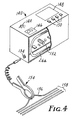
- Transmitter unit 140 includes housing 142 , output control switch 144 , output meter 146 , display 148 , and keys 150 .
- Output control switch 144 sets V+ and V- via variable power supply 22 .
- Output meter 146 is optional and merely measures the r.m.s. voltage (or current) of output signal 132 .
- Display 148 may be utilized in conjunction with logic circuitry (beyond the scope of the present invention) to set the frequencies of multi-frequency signal 12a .
- the cutaway in housing 142 reveals a printed circuit board 152 for receiving the various components of induction coil driver 10 , and also reveals antenna 26a , placed at the side of unit 140 to facilitate its use as an inductive coil.
- a remote inductive coupler 154 is also shown adjacent switching phone jack 134 , illustrating its use on a single wire 156 in cable group 158 .
- unit 140 includes a conventional portable power supply or battery pack (not shown), although an adapter could be provided for connection to an external power source.
Landscapes
- Engineering & Computer Science (AREA)
- Power Engineering (AREA)
- Computer Networks & Wireless Communication (AREA)
- Signal Processing (AREA)
- Amplifiers (AREA)
- Geophysics And Detection Of Objects (AREA)
- Details Of Aerials (AREA)
- Near-Field Transmission Systems (AREA)
Applications Claiming Priority (2)
| Application Number | Priority Date | Filing Date | Title |
|---|---|---|---|
| US07/317,820 US4914399A (en) | 1989-03-01 | 1989-03-01 | Induction coil driver |
| US317820 | 1989-03-01 |
Publications (2)
| Publication Number | Publication Date |
|---|---|
| EP0385672A2 true EP0385672A2 (de) | 1990-09-05 |
| EP0385672A3 EP0385672A3 (de) | 1991-03-13 |
Family
ID=23235407
Family Applications (1)
| Application Number | Title | Priority Date | Filing Date |
|---|---|---|---|
| EP19900301965 Withdrawn EP0385672A3 (de) | 1989-03-01 | 1990-02-23 | Treiber für eine Induktionsspule |
Country Status (6)
| Country | Link |
|---|---|
| US (1) | US4914399A (de) |
| EP (1) | EP0385672A3 (de) |
| JP (1) | JPH02278928A (de) |
| KR (1) | KR900015479A (de) |
| AU (1) | AU624474B2 (de) |
| CA (1) | CA2008442A1 (de) |
Families Citing this family (22)
| Publication number | Priority date | Publication date | Assignee | Title |
|---|---|---|---|---|
| DE4007566C2 (de) * | 1990-03-09 | 1998-07-16 | Siemens Ag | Leistungsverstärker für die Speisung einer Induktivität mit geschalteten Transistoren |
| US5187473A (en) * | 1990-08-31 | 1993-02-16 | Halliburton Company | Bipolar signal amplification or generation |
| US5920596A (en) * | 1995-01-31 | 1999-07-06 | Motorola, Inc. | Apparatus for amplifying a signal using a digital processor |
| US5886576A (en) * | 1996-10-16 | 1999-03-23 | Baxter International Inc. | Electrical power amplifier for continuous cardiac output monitoring |
| US6175272B1 (en) * | 1997-12-19 | 2001-01-16 | Nikon Corporation | Pulse—width modulation system |
| US6469919B1 (en) | 1999-07-22 | 2002-10-22 | Eni Technology, Inc. | Power supplies having protection circuits |
| US7180758B2 (en) * | 1999-07-22 | 2007-02-20 | Mks Instruments, Inc. | Class E amplifier with inductive clamp |
| US6819011B2 (en) * | 2002-11-14 | 2004-11-16 | Fyre Storm, Inc. | Switching power converter controller with watchdog timer |
| DE102005007803A1 (de) * | 2005-02-21 | 2006-08-24 | Robert Bosch Gmbh | Verfahren zur Detektion von in einem Medium eingeschlossenen Objekten sowie Messgerät zur Durchführung des Verfahrens |
| US7160426B2 (en) * | 2005-03-01 | 2007-01-09 | Wang Baosheng | Water treatment apparatus |
| US7288929B2 (en) * | 2005-07-19 | 2007-10-30 | Seektech, Inc. | Inductive clamp for applying signal to buried utilities |
| US7737671B2 (en) * | 2005-12-05 | 2010-06-15 | Texas Instruments Incorporated | System and method for implementing high-resolution delay |
| RU2008127063A (ru) * | 2005-12-20 | 2010-01-27 | Майнлэб Электроникс Пти Лимитед (AU) | Металлодетекторная платформа реального времени с прямоугольной формой передаваемого сигнала и выбираемыми пользователем параметрами передачи и приема |
| CN101089462B (zh) * | 2007-07-27 | 2010-06-02 | 极沣科技有限公司 | 载具的非接触发光显示装置 |
| US8344801B2 (en) | 2010-04-02 | 2013-01-01 | Mks Instruments, Inc. | Variable class characteristic amplifier |
| US9214901B2 (en) | 2012-07-27 | 2015-12-15 | Mks Instruments, Inc. | Wideband AFT power amplifier systems with frequency-based output transformer impedance balancing |
| CN103336306A (zh) * | 2013-06-25 | 2013-10-02 | 杭州展悦科技有限公司 | 一种用于管线探测的信号夹钳 |
| WO2015017476A1 (en) * | 2013-07-29 | 2015-02-05 | SeeScan, Inc. | Inductive clamp devices, systems, and methods |
| CA2946904C (en) * | 2014-03-24 | 2022-11-22 | Outer-Rim Developments Pty Ltd | High frequency modulated transmitter arrangement |
| US20160329885A1 (en) * | 2015-05-08 | 2016-11-10 | Hong Fu Jin Precision Industry (Shenzhen) Co., Ltd. | Signal processing circuit |
| ES3041928T3 (en) * | 2015-12-22 | 2025-11-17 | Thermatool Corp | High frequency power supply system with closely regulated output for heating a workpiece |
| US11783696B2 (en) * | 2019-10-18 | 2023-10-10 | Carrier Corporation | Fire detection system diagnostic systems and methods |
Family Cites Families (12)
| Publication number | Priority date | Publication date | Assignee | Title |
|---|---|---|---|---|
| CA993516A (en) * | 1974-12-17 | 1976-07-20 | Armond D. Cosman | Apparatus and system for locating buried objects |
| US4119908A (en) * | 1975-11-28 | 1978-10-10 | A. P. C. Industries, Inc. | Method for locating buried markers which are disposed along the path of an underground conductor |
| JPS5942492B2 (ja) * | 1976-11-18 | 1984-10-15 | ソニー株式会社 | プツシユプルパルス増巾回路 |
| US4322677A (en) * | 1979-03-16 | 1982-03-30 | Minnesota Mining And Manufacturing Company | System and method for locating resistive faults and interconnect errors in multi-conductor cables |
| US4387337A (en) * | 1979-11-07 | 1983-06-07 | Beeman Terrence M | Ground locating device for cathodically protected steel piping and/or electrical conduits |
| US4334227A (en) * | 1980-09-26 | 1982-06-08 | A.P.C. Industries, Inc. | Electronic marker device and method of making same |
| NL8203428A (nl) * | 1982-09-02 | 1984-04-02 | Philips Nv | Inrichting voor het omzetten van een elektrisch signaal in een akoestisch signaal. |
| JPS5967719A (ja) * | 1982-10-09 | 1984-04-17 | Nippon Gakki Seizo Kk | パルス幅変調回路 |
| DE3307689C2 (de) * | 1983-03-04 | 1984-12-20 | Standard Elektrik Lorenz Ag, 7000 Stuttgart | Schaltungsanordnung zum Betrieb eines induktiv arbeitenden Schienenkontakts |
| US4600891A (en) * | 1984-08-21 | 1986-07-15 | Peavey Electronics Corporation | Digital audio amplifier having a high power output level and low distortion |
| US4554512A (en) * | 1984-08-27 | 1985-11-19 | Aerotech, Inc. | Switching amplifier with MOSFET driver circuit |
| US4712094A (en) * | 1986-05-29 | 1987-12-08 | Minnesota Mining And Manufacturing Company | Self-orienting passive marker structure |
-
1989
- 1989-03-01 US US07/317,820 patent/US4914399A/en not_active Expired - Lifetime
-
1990
- 1990-01-24 CA CA002008442A patent/CA2008442A1/en not_active Abandoned
- 1990-02-01 AU AU48973/90A patent/AU624474B2/en not_active Ceased
- 1990-02-23 EP EP19900301965 patent/EP0385672A3/de not_active Withdrawn
- 1990-02-28 KR KR1019900002878A patent/KR900015479A/ko not_active Withdrawn
- 1990-02-28 JP JP2049128A patent/JPH02278928A/ja active Pending
Also Published As
| Publication number | Publication date |
|---|---|
| EP0385672A3 (de) | 1991-03-13 |
| US4914399A (en) | 1990-04-03 |
| JPH02278928A (ja) | 1990-11-15 |
| AU4897390A (en) | 1990-09-06 |
| KR900015479A (ko) | 1990-10-27 |
| CA2008442A1 (en) | 1990-09-01 |
| AU624474B2 (en) | 1992-06-11 |
Similar Documents
| Publication | Publication Date | Title |
|---|---|---|
| US4914399A (en) | Induction coil driver | |
| CA1163343A (en) | Method of, and apparatus for, inserting carrier frequency signal information onto distribution transformer primary winding | |
| US5469098A (en) | Isolated gate drive | |
| US6377163B1 (en) | Power line communication circuit | |
| US5986498A (en) | Audio direct from power supply | |
| US6922101B2 (en) | Phase shift modulation class D amplifier | |
| ATE136388T1 (de) | Elektromagnetisches detektor system | |
| JP3493537B2 (ja) | 無線電力伝送装置 | |
| EP0552598B1 (de) | Vorrichtung zum Schweissen medizinischer Kunststoffrohre | |
| FI84302B (fi) | Foerfarande och anordning foer lokalisering av en i jord eller vatten nedsaenkt kabels laege eller kabelfel fraon marken eller ovan vatten. | |
| US4541112A (en) | Electroacoustic transducer system | |
| US4141608A (en) | Circuitry for driving a non-linear transducer for ultrasonic cleaning | |
| US6608488B2 (en) | Apparatus for high voltage testing of insulated conductors and oscillator circuit for use with same | |
| EP0727900A2 (de) | Isolierte Hochimpedanz-Gleichstromquelle für Telekommunikationsanwendungen | |
| US5428295A (en) | Fault-locator for use in locating high-resistance ground faults in or on concentric-ground electrical power cables | |
| US4301499A (en) | Inverter circuit with current equalization | |
| US4387337A (en) | Ground locating device for cathodically protected steel piping and/or electrical conduits | |
| US3529150A (en) | Electronic track circuit for railway signalling | |
| US4767978A (en) | Hybrid switching circuit in a DC to DC converter | |
| US4233561A (en) | Automatic impedance matching conduit locator | |
| EP1088392B1 (de) | Sendeempfängerschaltung | |
| US4439738A (en) | Class D pulse width modulated amplifier | |
| EP1028522A1 (de) | Übertragungsvorrichtung | |
| FI84108C (fi) | Foerfarande och anordning foer lokalisering av kabelfel. | |
| EP0237303A1 (de) | Weckschaltung |
Legal Events
| Date | Code | Title | Description |
|---|---|---|---|
| PUAI | Public reference made under article 153(3) epc to a published international application that has entered the european phase |
Free format text: ORIGINAL CODE: 0009012 |
|
| AK | Designated contracting states |
Kind code of ref document: A2 Designated state(s): DE ES FR GB IT |
|
| PUAL | Search report despatched |
Free format text: ORIGINAL CODE: 0009013 |
|
| 17P | Request for examination filed |
Effective date: 19910102 |
|
| AK | Designated contracting states |
Kind code of ref document: A3 Designated state(s): DE ES FR GB IT |
|
| 17Q | First examination report despatched |
Effective date: 19930714 |
|
| STAA | Information on the status of an ep patent application or granted ep patent |
Free format text: STATUS: THE APPLICATION IS DEEMED TO BE WITHDRAWN |
|
| 18D | Application deemed to be withdrawn |
Effective date: 19940125 |