EP0385703A2 - Contrôle d'interface de clavier - Google Patents
Contrôle d'interface de clavier Download PDFInfo
- Publication number
- EP0385703A2 EP0385703A2 EP90302044A EP90302044A EP0385703A2 EP 0385703 A2 EP0385703 A2 EP 0385703A2 EP 90302044 A EP90302044 A EP 90302044A EP 90302044 A EP90302044 A EP 90302044A EP 0385703 A2 EP0385703 A2 EP 0385703A2
- Authority
- EP
- European Patent Office
- Prior art keywords
- keyboard
- data
- clock signal
- host processor
- receiving
- Prior art date
- Legal status (The legal status is an assumption and is not a legal conclusion. Google has not performed a legal analysis and makes no representation as to the accuracy of the status listed.)
- Withdrawn
Links
Images


Classifications
-
- G—PHYSICS
- G06—COMPUTING OR CALCULATING; COUNTING
- G06F—ELECTRIC DIGITAL DATA PROCESSING
- G06F3/00—Input arrangements for transferring data to be processed into a form capable of being handled by the computer; Output arrangements for transferring data from processing unit to output unit, e.g. interface arrangements
- G06F3/01—Input arrangements or combined input and output arrangements for interaction between user and computer
- G06F3/02—Input arrangements using manually operated switches, e.g. using keyboards or dials
- G06F3/023—Arrangements for converting discrete items of information into a coded form, e.g. arrangements for interpreting keyboard generated codes as alphanumeric codes, operand codes or instruction codes
Definitions
- the present application relates generally to data processing systems and more particularly to apparatus for controlling data transfer between a keyboard and its associated host processor.
- Prior art keyboards commonly contain logic to repetitively scan all keys and, in response to a detected change in key position, generate a scan code containing information descriptive of the keystroke.
- a scan code is available for transmission to the keyboard's associated system and if the associated system is configured to receive the keyboard data, the data is transmitted by the keyboard.
- Many keyboards transmit and receive this data serially in a synchronous fashion. This synchronous mode of data transmission typically requires the serial data stream, representing the keystroke information from the keyboard or command information to the keyboard, to be accompanied by a "clock" signal generated by the keyboard which allows the data to be properly received.
- the common method of controlling data transmission to and from such keyboards is by means of a single-chip microprocessor programmed to support the keyboard's serial interface and located in the system to which the keyboard is attached.
- the keyboard controller checks parity of a received byte, inserts a parity bit into a byte to be transmitted, translates the scan code from the keyboard into appropriate keystroke information and makes keystroke information and transmission error information available to the system.
- Such a microprocessor-based keyboard controller can represent a significant cost item in the price of the system.
- the cost of the microprocessor can become especially significant in regard to products, such as personal computers, which are highly competitive, price sensitive and involve high production volumes.
- the present invention enables the manufacturer of a design for keyboard interface control logic that is substantially less expensive to implement than prior art microprocessor based systems.
- the present invention is defined in the appended claims and relates to apparatus for handling data transfer between a synchronous keyboard and a system processor.
- the apparatus includes an asynchronous receiver/transmitter and associated control logic.
- keyboard control logic can be implemented at significantly lower cost compared to microprocessor-based keyboard controllers.
- FIG. 1 a simplified block diagram of a host/keyboard system is shown.
- the various signals commonly interchanged among the know elements in prior art keyboard communication systems are well understood and, for clarity of presentation, signals not relevant to the description and understanding of the invention have not been shown.
- Fig. 1 shows host processor 110 which sends data and commands to, and receives data from, keyboard interface control logic 120 via bus 101.
- Keyboard interface control logic 120 communicates with keyboard 130 via clock line 102 and data line 103.
- the typical ground and +5v lines between host 100 and keyboard 130 are not shown.
- Connector 140 provides the means of physical connection between the keyboard and the host system.
- keyboard interface control logic 120 would be a microprocessor, such as an Intel 8042, which would control keyboard protocol and handle the assembly, disassembly and interpretation of keyboard scan codes.
- keyboard interface control logic 120 performs the assembly/disassembly of the scan code byte while the host processor performs the interpretation of the scan code and the handling of the line protocol.
- the method and manner of interpreting scan codes and programming host processor 110 to implement the protocol discussed below are well understood by those of ordinary skill in the art.
- Keyboard 130 is a synchronous device which, as will be discussed, is implemented in a "pseudo-synchronous" system. Data is clocked in and out of the keyboard in accordance with clock line 102. The source of the signal on clock line 102 is controlled by keyboard interface control logic 120. As will be discussed in more detail below, keyboard interface control logic in conjunction with software signals from host 110 manipulates clock line 102 and data line 103 to achieve the receipt of data from and the providing of data to keyboard 130.
- the source of the data and clock lines is typically an open collector device located on the keyboard. Either the keyboard or the system can force the line low. When no communication is occurring, clock line 102 is generally held high. Keyboard transmission will not occur if the host has forced clock line 102 low.
- Data transmissions to and from the keyboard are sent serially over data line 103.
- Each transmission consists of 11 bits: a start bit, eight data bits, a parity bit and a stop bit. The method for accomplishing this transmission is discussed in more detail below.
- Keyboard interface control logic 120 requires no modification to the keyboard or its operations. Therefore, the keyboard will continue to operate in what appears to the keyboard to be its normal manner.
- the keyboard wants to send keystroke data to the host, it checks the clock and data lines for either a keyboard-inhibit (clock line low/data line high) or a request-to-send (clock line low/data line low) condition. If either of these conditions is present, the keyboard data is temporarily stored in the keyboard buffer until the next opportunity to transmit.
- the keyboard is permitted to output data and the eleven bits of the transmission are sent.
- the keyboard repetitively checks the clock line. If the clock line is pulled low by the host prior to the occurrence of the leading edge of the 10th bit (parity bit), the keyboard will stop its data transmission. If the clock line is pulled low after the occurrence of the leading edge of the 10th bit, the transmission will be completed. As discussed below, the host system will inhibit the keyboard after each transmission until the received data is processed and any necessary responses to the keyboard are sent.
- the keyboard will repetitively check the data clock lines for the request-to-send condition (data and clock lines both low).
- the host allows the clock line to return to a high condition.
- the keyboard will then clock in the 11 bits of the transmission.
- the keyboard indicates to the host that the data has been received by forcing the data line low after the 10th bit.
- the 11th (stop) bit is always high. Therefore, if the keyboard finds the data line low after the 10th received bit, an error has occurred and the keyboard will request that the data be resent from the host.
- the keyboard will respond to every transmission from the host by sending back a confirming transmission.
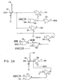
- Figs. 2A, 2B and 2C viewed together, comprise a schematic of keyboard interface control logic (KICL) 120.
- Fig 2A logic for controlling the keyboard clock and data lines is shown.
- the incoming clock signal on line 102 is provided through tristate buffer 201 to the TXC input of UART 220 (Fig. 2B) and through tristate buffer 207 to the RXC input of UART 220.
- the enabling input to buffer 201 is controlled by the output of gate 202.
- the keyboard clock signal is isolated from UART 220 when either ENABLE_TXC , indicating that the TXC input has been disabled, or TXMT, indicating that the UART 220 transmitter is empty (i.e. does not contain information awaiting transmission), are high.
- the output of gate 202 is inverted by inverter 203 and provided as ENTXC to gate 206 and tristate buffer 210.
- the clock signal seen at the TXC input of UART 220 is also controlled by the output of tristate buffer 204 in accordance with the output of gate 205.
- the output of buffer 204 can act as source of the clock signal to TXC by manipulation of the output of gate 205 by means of the signal DISABLE_CLK , indicating that the clock signal from the keyboard is disabled.
- the output of gate 205 is also controlled by RXRDY , indicating a received character is ready for input to the host, and ENTXC.
- IRQ_KBD is provided to host processor 110 to indicate whether or not UART 220 has received a character and requires service.
- Data is received from and sent to the keyboard over data line 103.
- Received data is supplied to the RXD input of UART 220 under control of tristate buffer 210, which is enabled and disabled by ENTXC.
- Serial data sent to the keyboard is provided from tristate buffer 211 under control of the output of gate 212.
- ENABLE_TXC is low, indicating the transmitter is enabled, the TXD serial data output from UART 220 will control the signal level seen at the enabling input of buffer 211 and, thereby, control the data signal provided to the keyboard.
- UART 220 shown in Fig 2B is in this embodiment a Signetics SCN2661 universal synchronous/asynchronous data communications controller. It will be understood that various other commercially available UART's could have been employed or that the functions of UART 220 could have been implemented in discrete logic.
- TXC is the clock signal used to transmit data from the UART. In this application, it is supplied externally.
- RXC is the clock signal used to clock received data into UART 220. Again, this signal is provided externally.
- CE is the chip enable signal, controlled by host processor 110.
- A0 and A1 are host processor 110 controlled lines to address one of the four internal UART 220 registers (mode register 1, mode register 2, command register and status register). RESET, controlled by the host processor, performs a master reset of the UART 220.
- R/W controlled by the host processor, determines the read or write condition of UART 220.
- RXD is the serial data input to the UART receiver.
- DSR is a general purpose input implemented to force a low condition at TXEMT if ENABLE_TXC goes low.
- TXEMT indicates whether the transmitter has completed serialization of the last character received from the host.
- RXRDY indicates whether the receive data holding register has a character ready for reading by the host.
- D0-D7 provide the 8-bit parallel path for transfer of data, commands and status between UART 220 and host processor 110.
- TXD is the serial data output from the transmitter.
- DTR is a general purpose output, controlled by host processor 110 by means of the UART 220 command register. DTR is implemented to control whether or not TXEMT is allowed to inhibit keyboard data transmission. When UART 220 is configured to receive data, DTR will be low.
- TXEMT and DTR are provided to gate 221, the output of which is provided as the data input to register 222.
- the Q output of register 222 is in turn connected to the data input of register 223.
- the TXC clock signal from buffer 201 is provided as the clocking signal to registers 222 and 223. Whenever ENABLE_TXC is low to gate 225, indicating the UART 220 transmitter is not enabled, register 223 will hold TXMT high.
- registers 222 and 223 The general function of registers 222 and 223 is to delay the generation of TXMT, indicating that the transmitter is empty, for two TXC clock times. This is necessary since UART 220 is not operating in a synchronous mode compatible with the typical synchronous operating mode of keyboard 130. TXEMT from UART 220 would normally indicate that the transmitter is empty after nine bits of data have been transmitted. To ensure that the final two bits (parity and stop bits) of the eleven bit transmission are transmitted, the transmitter empty signal must be delayed beyond its normal generation time.
- Logic for generation of the DISABLE_CLK and ENABLE_TXC signals is shown in Fig. 2C. Both signals can be generated under the control of host processor 110 by means of data signal SIO0 and clocking signals CS_DISCLK and CS_EN_TXC provided by host 110. As explained in more detail below, the ability to enable/disable the keyboard clock and the UART transmitter are useful in coordinating data transfer between the keyboard and UART 220.
- the output of gate 232 is connected to the reset input of register 230 and the set input of register 231.
- RST-KBD indicating keyboard reset, will remain high during normal system operations. Therefore, during normal operations, TXMT going low during transmission to the keyboard, indicating that the UART transmitter is empty, will operate to force DISABLE_CLK low, thereby disabling the keyboard clock, and force ENABLE_TXC high, thereby preventing the keyboard clock from being passed through to the UART 220 TXC input.
- clock line 102 and data line 103 The states of clock line 102 and data line 103, and therefore the transfer of data to and from the keyboard, is under the control of host processor 110.
- the typical clock and data line protocol is given below: CLOCK DATA INTERFACE CONTROL H H KEYBOARD PERMITTED TO OUTPUT DATA L H KEYBOARD INHIBITED FROM OUTPUTTING DATA L L HOST REQUESTS TO SEND TO KEYBOARD H L KEYBOARD PERMITTED TO RECEIVE DATA
- the keyboard When the keyboard is ready to transmit data to the host. it checks the status of the data and clock lines. If a keyboard inhibit or request-to-send is detected, the data is stored in the keyboard data buffer until the data and clock lines allow transmission. If the data and clock lines are both high, the keyboard clocks out the 11 bit serial data stream. The keyboard continues to periodically check the clock line during the data transmission and, if the line has been forced low by the host and the transmission in not beyond the leading edge of the 10th bit, the keyboard will terminate the transmission.
- the host system when configuring itself into a condition to accept data from the keyboard, the host system will perform the following steps: (a) ensure that the keyboard will not attempt to send additional data by forcing clock line 102 low (by clocking a low signal on line SIO0 into register 230), (b) disable TXC by clocking a high signal on line SIO0 into register 231, (c) enable the UART 220 receiver by setting the proper bits in the UART command register and (d) release the keyboard to drive the clock signal on line 102 by clocking a high signal on line SIO0 into register 230.
- KICL 120 when in the condition to receive data from the keyboard, KICL 120 will be configured with buffers 201, 204 and 211 disabled and buffers 207 and 210 enabled, thereby allowing data from keyboard 130 to be passed through to the RXD input of UART 220 and the clock signal from keyboard 130 to be passed through to the RXC input.
- the host system will perform the following steps: (a) further transmission from the keyboard will be temporarily inhibited by forcing clock line 102 low (by forcing DISABLE_CLK low), (b) the received scan code will be transmitted to host processor 110, (c) host processor 110 will determine if the received scan code requires a transmission back to the keyboard, (d) if a transmission to the keyboard is required, the transmitting procedure, discussed below, will be initiated, and (e) if no transmission to the keyboard is required, the keyboard will be reenabled by returning the clock line high (by driving DISABLE_CLK high).
- UART 220 and keyboard 130 are not directly compatible and therefore cannot communicate without benefit of KICL 120.
- the particular protocol for sending data to the keyboard involves generation of pseudo-clock signals to ensure proper data handling by UART 220.
- the UART 220 receiver and transmitter are disabled by setting the proper bits in the UART command register, (b) the data from host processor 110 is loaded into the UART 220 transmit holding register, (c) the transmitter is enabled by setting the proper bit in the command register, (d) TXC is enabled by forcing ENABLE_TXC low, thereby generating a falling edge of TXC, (e) after an appropriate time interval (a minimum of 0.5 microseconds in this embodiment), disable TXC, (e) after another similar time interval, again enable TXC, thereby generating a second falling edge of TXC, (f) after another similar time interval, again disabling TXC, (g) after another similar time interval, again enabling TXC, thereby generating a third falling edge of TXC (The "start" bit will be output from the TXD output of UART 220 at this point.
- This bit always low, brings data line 103 low.
- the clock and data lines are both now low, indicating that the host requests to send data to the keyboard.), (h) after a suitable interval (in this embodiment, a minimum of 60 microseconds), releasing the keyboard clock by forcing DISABLE_CLK high, allowing the keyboard to clock in the data, (i) checking status of the transmission by monitoring ENABLE_TXC, and (j) when the transmission is completed, configuring the system for receiving the next scan code from the keyboard. Normally, the keyboard will respond to each transmission from the host by sending an acknowledgement scan code.
Landscapes
- Engineering & Computer Science (AREA)
- General Engineering & Computer Science (AREA)
- Theoretical Computer Science (AREA)
- Human Computer Interaction (AREA)
- Physics & Mathematics (AREA)
- General Physics & Mathematics (AREA)
- Input From Keyboards Or The Like (AREA)
- Communication Control (AREA)
Applications Claiming Priority (2)
| Application Number | Priority Date | Filing Date | Title |
|---|---|---|---|
| US07/316,357 US5146584A (en) | 1989-02-27 | 1989-02-27 | Keyboard interface system allowing a synchronous keyboard to communicate with a host processor asynchronously by manipulating the keyboard clock's state |
| US316357 | 1994-10-03 |
Publications (2)
| Publication Number | Publication Date |
|---|---|
| EP0385703A2 true EP0385703A2 (fr) | 1990-09-05 |
| EP0385703A3 EP0385703A3 (fr) | 1992-06-24 |
Family
ID=23228719
Family Applications (1)
| Application Number | Title | Priority Date | Filing Date |
|---|---|---|---|
| EP19900302044 Withdrawn EP0385703A3 (fr) | 1989-02-27 | 1990-02-27 | Contrôle d'interface de clavier |
Country Status (2)
| Country | Link |
|---|---|
| US (1) | US5146584A (fr) |
| EP (1) | EP0385703A3 (fr) |
Cited By (1)
| Publication number | Priority date | Publication date | Assignee | Title |
|---|---|---|---|---|
| EP0414357A3 (en) * | 1989-08-22 | 1992-06-24 | Acer Incorporated | Keyboard interface |
Families Citing this family (5)
| Publication number | Priority date | Publication date | Assignee | Title |
|---|---|---|---|---|
| US5222228A (en) * | 1990-12-14 | 1993-06-22 | Cybex Corporation | Character and signal generator for detecting keyboard disconnected condition generated by an interrupted booting process and generating signal indicating that keyboard is now coupled thereto |
| JPH07111670B2 (ja) * | 1991-03-12 | 1995-11-29 | インターナショナル・ビジネス・マシーンズ・コーポレイション | コントローラ、通信インターフェース、およびデータ伝送を制御する方法 |
| US5418825A (en) * | 1992-09-16 | 1995-05-23 | Texas Instruments Incorporated | Time-domain boundary bridge method and apparatus |
| JPH08212151A (ja) * | 1995-02-08 | 1996-08-20 | Canon Inc | 情報処理機器 |
| CN100340953C (zh) * | 2005-01-13 | 2007-10-03 | 中国科学院长春光学精密机械与物理研究所 | 数字信号处理器与标准计算机键盘的接口装置 |
Family Cites Families (4)
| Publication number | Priority date | Publication date | Assignee | Title |
|---|---|---|---|---|
| GB2101859A (en) * | 1981-04-22 | 1983-01-19 | Pitney Bowes Inc | Display processor for use in a word processing system |
| US4460957A (en) * | 1981-08-12 | 1984-07-17 | International Business Machines Corporation | Self-pacing serial keyboard interface for data processing system |
| JPS59123336A (ja) * | 1982-12-28 | 1984-07-17 | インタ−ナシヨナル ビジネス マシ−ンズ コ−ポレ−シヨン | 直列キ−ボ−ド・インタフエ−ス・システム |
| US4964075A (en) * | 1987-05-08 | 1990-10-16 | A. J. Weiner, Inc. | Software and hardware independent auxiliary user programmable intelligent keyboard |
-
1989
- 1989-02-27 US US07/316,357 patent/US5146584A/en not_active Expired - Lifetime
-
1990
- 1990-02-27 EP EP19900302044 patent/EP0385703A3/fr not_active Withdrawn
Cited By (1)
| Publication number | Priority date | Publication date | Assignee | Title |
|---|---|---|---|---|
| EP0414357A3 (en) * | 1989-08-22 | 1992-06-24 | Acer Incorporated | Keyboard interface |
Also Published As
| Publication number | Publication date |
|---|---|
| EP0385703A3 (fr) | 1992-06-24 |
| US5146584A (en) | 1992-09-08 |
Similar Documents
| Publication | Publication Date | Title |
|---|---|---|
| US5790895A (en) | Modem sharing | |
| EP0071747B1 (fr) | Interface sérielle d'un clavier à horloge autonome pour un système de traitement de données | |
| US5600793A (en) | Method and system of bi-directional parallel port data transfer between data processing systems | |
| EP0189638B1 (fr) | Adaptateur de largeur de bus | |
| US6070204A (en) | Method and apparatus for using universal serial bus keyboard to control DOS operations | |
| EP0335424B1 (fr) | Dispositif de vérification de parité | |
| EP1546898B1 (fr) | Dispositf de circuit integre a interface pour connexion usb | |
| US5797038A (en) | Method and system for serially based host/peripheral communication | |
| US8099529B1 (en) | Software based native command queuing utilizing direct memory access transfer context information | |
| US5068785A (en) | Bus control for small computer system interface with transfer indication preceding final word transfer and buffer empty indication preceding receipt acknowledgement | |
| US4779190A (en) | Communication bus interface | |
| US6098120A (en) | Peripheral sharing system using a bus bridge to emulate peripherals on a first bus to a host on a second bus | |
| JPH09179812A (ja) | 情報処理システム及びその制御方法 | |
| EP0311760A2 (fr) | Circuit de commande pour transmission en parallèle de données à grande vitesse | |
| US6366877B1 (en) | Method and device for emulation of peripheral input/output (I/O) controller of a computer system | |
| JP3609051B2 (ja) | Usb−hubデバイスおよびその制御方法 | |
| EP0385703A2 (fr) | Contrôle d'interface de clavier | |
| EP0139254A2 (fr) | Appareil et méthode pour un transfert direct de données de mémoire vers un dispositif périphérique et du dispositif périphérique vers la mémoire | |
| DK170081B1 (da) | Dataoverføringskredsløb | |
| US6772238B2 (en) | Parallel port with direct memory access capabilities | |
| EP0464729A2 (fr) | Circuit logique d'une interface de bus SCSI pour le traitement de code d'identification | |
| JP2000076178A (ja) | ブロック・モ―ドで動作する装置間の、通信リンクによるバ―スト・モ―ド・デ―タ転送の自動化制御 | |
| US5218683A (en) | Method and apparatus for concealing the enablement of a device by modifying a status word | |
| US6654845B1 (en) | System and method implementing a secondary bus to avoid read data latency | |
| US20050144331A1 (en) | On-chip serialized peripheral bus system and operating method thereof |
Legal Events
| Date | Code | Title | Description |
|---|---|---|---|
| PUAI | Public reference made under article 153(3) epc to a published international application that has entered the european phase |
Free format text: ORIGINAL CODE: 0009012 |
|
| AK | Designated contracting states |
Kind code of ref document: A2 Designated state(s): DE FR GB |
|
| PUAL | Search report despatched |
Free format text: ORIGINAL CODE: 0009013 |
|
| AK | Designated contracting states |
Kind code of ref document: A3 Designated state(s): DE FR GB |
|
| STAA | Information on the status of an ep patent application or granted ep patent |
Free format text: STATUS: THE APPLICATION IS DEEMED TO BE WITHDRAWN |
|
| 18D | Application deemed to be withdrawn |
Effective date: 19921228 |