EP0385885A1 - Frequenz-Codierungssystem mit Hochsicherheitsbetriebsart - Google Patents
Frequenz-Codierungssystem mit Hochsicherheitsbetriebsart Download PDFInfo
- Publication number
- EP0385885A1 EP0385885A1 EP90420077A EP90420077A EP0385885A1 EP 0385885 A1 EP0385885 A1 EP 0385885A1 EP 90420077 A EP90420077 A EP 90420077A EP 90420077 A EP90420077 A EP 90420077A EP 0385885 A1 EP0385885 A1 EP 0385885A1
- Authority
- EP
- European Patent Office
- Prior art keywords
- output
- test
- frequency
- outputs
- inputs
- Prior art date
- Legal status (The legal status is an assumption and is not a legal conclusion. Google has not performed a legal analysis and makes no representation as to the accuracy of the status listed.)
- Ceased
Links
Images


Classifications
-
- G—PHYSICS
- G06—COMPUTING OR CALCULATING; COUNTING
- G06F—ELECTRIC DIGITAL DATA PROCESSING
- G06F11/00—Error detection; Error correction; Monitoring
- G06F11/07—Responding to the occurrence of a fault, e.g. fault tolerance
- G06F11/0796—Safety measures, i.e. ensuring safe condition in the event of error, e.g. for controlling element
-
- G—PHYSICS
- G05—CONTROLLING; REGULATING
- G05B—CONTROL OR REGULATING SYSTEMS IN GENERAL; FUNCTIONAL ELEMENTS OF SUCH SYSTEMS; MONITORING OR TESTING ARRANGEMENTS FOR SUCH SYSTEMS OR ELEMENTS
- G05B9/00—Safety arrangements
- G05B9/02—Safety arrangements electric
-
- G—PHYSICS
- G06—COMPUTING OR CALCULATING; COUNTING
- G06F—ELECTRIC DIGITAL DATA PROCESSING
- G06F11/00—Error detection; Error correction; Monitoring
- G06F11/07—Responding to the occurrence of a fault, e.g. fault tolerance
- G06F11/08—Error detection or correction by redundancy in data representation, e.g. by using checking codes
- G06F11/10—Adding special bits or symbols to the coded information, e.g. parity check, casting out 9's or 11's
-
- G—PHYSICS
- G06—COMPUTING OR CALCULATING; COUNTING
- G06F—ELECTRIC DIGITAL DATA PROCESSING
- G06F11/00—Error detection; Error correction; Monitoring
- G06F11/07—Responding to the occurrence of a fault, e.g. fault tolerance
- G06F11/16—Error detection or correction of the data by redundancy in hardware
- G06F11/18—Error detection or correction of the data by redundancy in hardware using passive fault-masking of the redundant circuits
- G06F11/187—Voting techniques
Definitions
- the invention relates to a frequency coding system with high operational reliability.
- Oriented fault logic systems, or dynamic safety logic systems, intended to control actuators reliably according to a predetermined number of logic information, are very widely used in monitoring or control devices in which security plays a fundamental role.
- the invention aims to allow a significant reduction in the size of such systems without changing the operating principle.
- such circuits cannot directly replace the logic part of a oriented fault logic system because they supply binary signals which are not compatible with the frequency control of the actuators of a oriented fault logic system. .
- a frequency coding system with high operational reliability characterized in that it comprises a frequency input connected to the output of a frequency generator whose frequency F is included in a predetermined range of frequencies, at least one output associated with one or more inputs to which the binary coded output signals of a self-test logic circuit are applied, the system output signals being intended to control actuators, the system consisting of a plurality of semiconductor components, comprising switches controlled by the system input signals, interconnected so that: - in the absence of a fault in the system, an output signal of frequency F, called an unsafe output signal, corresponds to a first predetermined logic state of the associated binary input signal (s), and a continuous output signal or frequency not included in said predetermined range, called safe output signal, corresponds to a second predetermined logic state of the associated binary input signal (s) , - a simple failure inside the system does not modify its behavior or produce a safe output signal at output and - a fault is detected by a fault detector before another fault occurs, the system consisting of a plurality of semiconductor components,
- Such a system preferably comprises at least two controlled switches, the control electrodes of which are connected to predetermined inputs of the system, arranged in series between the frequency generator and the output associated with said inputs, and of which only simultaneous conduction allows the connection between the output and the frequency generator.
- the frequency coding system is connected to the outputs of a self-testing logic circuit 10.
- This circuit is designed so as to deliver n information bits, or functional bits, I1 to In, and k coding bits, C1 to Ck. It can also provide error indication bits M, grouped in pairs, the two bits of a pair being identical (0.0 or 1.1) when an error associated with this pair is detected in the self-test circuit. .
- the coding system is designed so that an output, S1 to Sn, of the system, intended for controlling an actuator (not shown), is associated with each of the outputs of the self-test circuit delivering an information bit , I1 to In.
- the functional binary outputs, I1 to In, of the self-testing circuit must be transformed into frequency-coded outputs S1 to Sn, a signal of predetermined frequency F being present on an output Si when the associated input signal Ii is at logical state 1.
- the coding system comprises a frequency generator 12 producing an alternating signal whose frequency F is included in a predetermined range of frequencies.
- the system represented in FIG. 1 is a so-called “fail-safe” system.
- An output signal of frequency F corresponds to a state considered to be insecure, its accidental presence being able to lead downstream of the system to a dangerous situation.
- any continuous output signal or frequency other than F that is to say not belonging to the aforementioned range of frequencies, is considered as safe.
- an output must be in a safe state in the absence of failure, cannot go into an unsafe state in the presence of a single fault belonging to a set of listed simple faults likely affect the system components.
- any erroneous output produced by a fault must be an output whose state is safe.
- each branch of the system disposed between the frequency generator 12 and an output Si, comprises at least two controlled switches of which only the simultaneous activation authorizes a connection between the frequency generator and the output considered.
- the output S1 is connected to the generator 12 by two field effect transistors T1 and T2 arranged in series and the gates of which are both connected to the associated output I1 of the self-test circuit 10.
- a frequency signal F cannot be present on the output S1 only when the input signal I1 is in logic state 1, making the two transistors T1 and T2 simultaneously conductive.
- the transistors T1 and T2 are blocked and the link is interrupted between the frequency generator 12 and the output S1. Due to the redundancy, the aforementioned simple failure, constituted by the bonding of one of the transistors T1 or T2 in the conduction position, cannot lead to an unsafe output.
- the point 16 common to all the branches is connected to the generator 12 by means of a field effect transistor T4, the gate of which is connected to the output of a logic gate 18, of the EXCLUSIVE OR type.
- the two input signals (F1 and F2) of the logic gate 18 are different, its output A is in the logic state 1 and the transistor T4 is conductive.
- a controller 20 receives as input both the information bits, I1 to In, and the coding bits, C1 to Ck, supplied by the self-test logic circuit 10. If the information is coded by a parity code, there is is a parity checker. If, as in the embodiment according to FIG. 1, they are coded by means of a Berger code, the controller 20 is a Berger controller, of known type. Such a controller reconstructs coding bits from the information bits which it receives and compares these reconstituted coding bits with the coding bits, C1 to Ck, which are supplied to it by the circuit 10. If the codes are not identical, the controller considers that the information transmitted by the self-test circuit 10 is incorrect and produces two identical bits (0.0 or 1.1).
- the controller 22 receives not only the outputs from the controller 20, but also the error indication bits M produced by the self-test circuit.
- the output A of the gate 18 then goes to the logic state 0, blocking the transistor T4 and interrupting the links between the frequency generator 12 and all the outputs, S1 to Sn of the system which are thus automatically placed in a state sure.
- the transistors T1 and T2 are blocked, the transistors T3 and T4 are conductive and the output Si is at 0.
- the transistors T1, T2 and T4 are conductive , the transistor T3 is blocked and the output signal Si is a frequency signal F.
- FIG. 5 represents a safe frequency coding system intended to be connected to a self-testing circuit 10 whose outputs are duplicated.
- the circuit 10 comprises two subsystems 24 and 26, the outputs I1i and I2i of which are identical in the absence of a fault inside the self-test circuit.
- Each branch of the system is constituted as previously by two transistors T1 and T2 arranged in series between the frequency generator 12 and an output Si.
- the gate of the first transistor T1 of a branch is connected to the output I1i of the subsystem 24, while the gate of the second transistor T2 is connected to the corresponding output I2i of the subsystem 26.
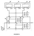
- FIG. 6 there is shown a secure frequency coding system intended to be connected to a self-test circuit 10 whose outputs are triplicated.
- Circuit 10 comprises three subsystems 28, 30 and 32, the outputs I1i, I2i and I3i of which are identical in the absence of a fault inside the self-test circuit.
- Each branch of the system, connecting an output Si to the frequency generator 12, is constituted by the parallel connection of three elementary branches 34, 36 and 38.
- Each elementary branch comprises, as in the previous systems, two transistors T1 and T2 arranged in series between the frequency generator 12 and the output Si.
- the gates of the transistors T1 and T2 of the first elementary branch 34 are connected respectively to the outputs I1i and I3i of the subsystems 28 and 32.
- the gates of the transistors T1 and T2 of the second elementary branch 36 are connected respectively to the outputs I1i and I2i of the subsystems 28 and 30, while the gates of the transistors T1 and T2 of the third elementary branch 38 are connected respectively to the outputs I2i and I3i of the subsystems 30 and 32
- its three outputs I1i, I2i and I3i are identical and the three elementary branches are include as a branch of the systems described above, connecting the output S1 to the generator 12 when the outputs of the circuit 10 are at 1 and interrupting this connection when they are at 0.
- the hardware redundancy of the three elementary branches makes it possible to obtain the expected result at the output even if one of the outputs of the self-test circuit 10 is erroneous.
- the system indeed performs a majority vote between its three associated inputs I1i, I2i and I3i and provides an output Si corresponding to the logic state of the two inputs which are identical.
- each elementary branch is connected to ground via two transistors T3 and T ⁇ 3 arranged in series and controlled respectively, after inversion, by the signals applied to the gates of the transistors T1 and T2 of said elementary branch.
- a simple failure cannot lead to an unsafe state at the output.
- a multiple fault constituted by the superposition of several simple faults can, in certain cases, lead to an unwanted connection of an output and of the frequency generator.
- the simultaneous bonding to 1 of the gate of T4 and of the input I1 leads to an unsafe, undesired state, of the output S1 when the input I1 should be in logical state 0.
- Additional measures must therefore be taken to obtain a system with high operational safety (“strongly fail safe”), ie a system which remains safe even in the presence of failures multiple.
- strongly fail safe strongly fail safe
- a secure coding system is supplemented so as to ensure the detection of a fault, by a fault detector, before another fault occurs, the combination of which with the first would be capable of producing an output signal. wrong not sure.
- the fault detector interrupts the link between the frequency generator and all of the system outputs when a fault is detected. It should be noted that it is not essential that the fault detector detects all the simple faults likely to occur in the system, but that the system must remain safe in the presence of a simple undetectable fault.
- BIST Bus in self test
- FIG. 7 represents an exemplary embodiment of a coding system with high operational reliability developed from a system according to FIG. 1.
- the self-test circuit 10 the controllers 20 and 22 have been put on the figure.
- a test vector generator (GVT) 40 used for the offline test of the system, produces a test sequence intended to highlight at least all the simple faults likely to cause an erroneous incorrect output signal in combination with a subsequent failure.
- the test vector generator has 5 outputs A1, A2, A3, A4, A5, connected to test points of the system, respectively at the input of the inverter 14, to the gate of the tansistors T2 and T1 of each branch of the system, and to the two inputs of the logic gate 18. In the embodiment shown, these connections are made via transistors 42 whose gates receive a test signal T throughout the duration of a test sequence. In addition, transistors 44, whose gate receives a signal complementary to the test signal, are arranged between each of the test points and the associated output (I1 to In) of the self-test circuit 10 or F1, F2 of the controller 22.
- a transistor T5 the gate of which is connected to the output of an inverter 45, the input of which receives the test signal T, is connected between the frequency generator 12 and the transistor T4.
- the transistors 44 are conductive and the test points are normally connected to the corresponding inputs (Ii, F1, F2) of the system, while during a test sequence the transistors 44 are blocked. isolating the test points from the corresponding inputs of the system and the transistors 42 are conductive, thus connecting the test points to the outputs of the test vector generator.
- the entire system is also isolated from the frequency generator, due to the blocking of transistor T5, during the test sequence.
- a test vector is formed by the set of binary signals present at a given time on the outputs A1 to A5 of the test vector generator 40. During a test sequence, this generates a predetermined sequence of the test vector, whose constitution and succession are such that all faults to be detected can be highlighted by observation of a certain number of test outputs.
- each branch has a test output Ei arranged at the common point between the transistors T1 and T2.
- Test outputs E11 and E12 are located on either side of the transistor T4, in the part common to all the branches.
- the test circuit is completed by transistors T6 and T7 arranged in series between the output Si and the supply voltage corresponding to the logic state 1.
- the gate of the transistor T6 is connected to the input of the inverter 14 and the gate of transistor T7 to the test signal T.
- the transistor T7 is always in conduction state and, when the test signal A1 is in logic state 0, the transistor T6 is blocked and transistor T3 conductive, forcing output Si to 0.
- transistor T6 is conductive and transistor T3 blocked, forcing output Si to 1.
- the logic states of the test outputs E1 to En, E11 and E12 are a function of the test vectors applied to the system and of the presence or absence of faults in the system.
- a test output may be floating, that is to say in none of the predetermined logic states 0 to 1. This is the case, for example, of the test output Ei when neither the transistor T1 nor the transistor T2 are conductive. To eliminate any uncertainty, the holding transistors, shown in FIG. 8, are available at each of the test output points.
- holding transistors have the function of maintaining a point of the circuit in the previous logic state when this point is isolated from the rest of the circuit.
- a first transistor TM1 connected between the point considered and the positive supply voltage corresponding to the logic state 1, and the gate of which is connected to the point considered, and a second transistor TM2, connected between said point and the ground, and whose gate is connected to the previous one by an inverter 46.
- the transistor TM2 is conductive and the point remains at ground if it is isolated from the rest of the circuit, while if point E is in logic state 1 it is the transistor TM1 which is conductive and maintains it in this logic state in case of isolation of the rest of the circuit. It can be checked that the faults likely to appear in these holding transistors maintain their safety quality to the system.
- the test outputs E1 to En, E11 and E12 are connected to the inputs of a signature analyzer 48.
- the signature analyzer of known type, constituted by a loopback register, produces in G1 a signature from the logic states successive test outputs applied to it during a test sequence.
- the signature analyzer will be designed and initialized at the start of a test sequence, so that, in the absence of a failure in the system, the final signature obtained is a series of bits where alternate the 1 and the 0, for example 010101 ...
- a complementary circuit 50 serving as a reference generates in G2 a complementary reference signature (10101 ).
- Signals G1 and G2 are applied to the global dual-rail controller 22 ( Figure 1).
- the controller 22 produces identical bits F1 and F2 and the output A of the gate 18 goes to the state logic 0, blocking transistor T4 and putting outputs S1 to Sn in a safe state.
- the table below illustrates a sequence of test vectors making it possible to detect all the faults likely to occur in the system represented in FIGS. 7 and 8, except the bonding in the blocked position of the transistor T4. This last fault may not be detected because it automatically interrupts the link between the frequency generator 12 and the outputs S1 to Sn of the system.
- the logical states expected from the test outputs Ei, E11 and E12 and from signal A have also been indicated in the table in the absence of a fault in the system. Test Vector No.
- A1 A2 A3 A4 AT 5 AT Yes Ei E11 E12 1 1 1 1 1 1 0 1 1 1 1 1 2 0 1 1 1 0 1 0 0 0 0 3 1 1 1 0 0 0 1 1 1 0 4 0 1 1 0 1 1 0 0 0 0 5 1 1 1 0 1 1 1 1 1 6 0 1 1 1 1 0 0 0 0 1 7 1 1 0 1 1 1 0 1 1 0 1 8 0 0 0 0 0 0 0 1 0 1
- all the elements of the fault detector namely the test vector generator 40, the signature analyzer 48 and the complementary circuit 50, operate at a very high frequency compared to the frequency F.
- the frequency F may be of the order of 1 kHz and the clock frequency of the elements of the fault detector is greater than 20 kHz.
- this frequency is of the order of 1 MHz. Normal operation of the system can therefore be interrupted for a very short time, duration of the test signal T, to allow a test sequence.
- Modifications at high frequency of the output signals S1 to Sn due to a test sequence are considered as interference by the actuators located downstream of the system and do not disturb their operation.
- the test sequences are repeated periodically with a period much less than the average time between two failures ("MTBF").
- MTBF average time between two failures
- several test sequences are carried out during a half-period of the output signal of the frequency generator 12. It must nevertheless be ensured that the test sequence is not carried out at the time of a change of state of the signal of frequency generator output. This can be done very simply by synchronizing the test signal T with the frequency signal F.
- the controlled switches of the system are preferably constituted by field effect transistors with an insulated gate type of tyoe MOSFET and the entire system and the self-testing logic circuit can be integrated on the same wafer.
- the invention is in no way limited to the particular embodiments shown.
- the principles described allow the creation of coding systems with high operational reliability intended to code the outputs of the self-testing circuit whatever the type of coding adopted.
- the structure of the fault detector and the sequence of test vectors will also be adapted according to the type of coding of the information at the input of the system and the set of listed faults likely to occur.
Landscapes
- Engineering & Computer Science (AREA)
- Physics & Mathematics (AREA)
- General Physics & Mathematics (AREA)
- Theoretical Computer Science (AREA)
- Quality & Reliability (AREA)
- General Engineering & Computer Science (AREA)
- Automation & Control Theory (AREA)
- Tests Of Electronic Circuits (AREA)
Applications Claiming Priority (2)
| Application Number | Priority Date | Filing Date | Title |
|---|---|---|---|
| FR8902638 | 1989-02-27 | ||
| FR8902638A FR2643762B1 (fr) | 1989-02-27 | 1989-02-27 | Systeme de codage en frequence a haute surete de fonctionnement |
Publications (1)
| Publication Number | Publication Date |
|---|---|
| EP0385885A1 true EP0385885A1 (de) | 1990-09-05 |
Family
ID=9379240
Family Applications (1)
| Application Number | Title | Priority Date | Filing Date |
|---|---|---|---|
| EP90420077A Ceased EP0385885A1 (de) | 1989-02-27 | 1990-02-14 | Frequenz-Codierungssystem mit Hochsicherheitsbetriebsart |
Country Status (2)
| Country | Link |
|---|---|
| EP (1) | EP0385885A1 (de) |
| FR (1) | FR2643762B1 (de) |
Cited By (3)
| Publication number | Priority date | Publication date | Assignee | Title |
|---|---|---|---|---|
| EP0526350A1 (de) * | 1991-07-29 | 1993-02-03 | Schneider Electric Sa | Kompakte und fehlertolerante Schnittstelle und deren Verwendung in einer Mehrheitsentscheidungsvorrichtung |
| WO1995006908A1 (en) * | 1993-09-02 | 1995-03-09 | Sofia Koloni Ltd. | Strongly fail-safe interface based on concurrent checking |
| US5930254A (en) * | 1991-11-08 | 1999-07-27 | Teledesic Llc | Non-blocking dynamic fast packet switch for satellite communication system |
Citations (5)
| Publication number | Priority date | Publication date | Assignee | Title |
|---|---|---|---|---|
| FR1266500A (fr) * | 1960-05-20 | 1961-07-17 | Alsacienne Constr Meca | Commutateur électronique à haute sécurité |
| US3600604A (en) * | 1968-12-03 | 1971-08-17 | Westinghouse Electric Corp | Failsafe logic gates |
| EP0101037A2 (de) * | 1982-08-09 | 1984-02-22 | Hitachi, Ltd. | Logische Schaltung |
| DE3519252A1 (de) * | 1985-05-29 | 1986-12-04 | Fresenius AG, 6380 Bad Homburg | Fehlersichere logikschaltung |
| DE3621022A1 (de) * | 1986-06-20 | 1987-12-23 | Licentia Gmbh | Fehlersicheres und-glied |
-
1989
- 1989-02-27 FR FR8902638A patent/FR2643762B1/fr not_active Expired - Lifetime
-
1990
- 1990-02-14 EP EP90420077A patent/EP0385885A1/de not_active Ceased
Patent Citations (5)
| Publication number | Priority date | Publication date | Assignee | Title |
|---|---|---|---|---|
| FR1266500A (fr) * | 1960-05-20 | 1961-07-17 | Alsacienne Constr Meca | Commutateur électronique à haute sécurité |
| US3600604A (en) * | 1968-12-03 | 1971-08-17 | Westinghouse Electric Corp | Failsafe logic gates |
| EP0101037A2 (de) * | 1982-08-09 | 1984-02-22 | Hitachi, Ltd. | Logische Schaltung |
| DE3519252A1 (de) * | 1985-05-29 | 1986-12-04 | Fresenius AG, 6380 Bad Homburg | Fehlersichere logikschaltung |
| DE3621022A1 (de) * | 1986-06-20 | 1987-12-23 | Licentia Gmbh | Fehlersicheres und-glied |
Non-Patent Citations (1)
| Title |
|---|
| PROCEEDINGS OF THE EIGHTH INTERNATIONAL SYMPOSIUM ON MULTIPLE-VALUED LOGIC 1978, ROSEMONT,ILLINOIS,US pages 287 - 295; J.E.SMITH AND J.DUSSAULT: "FAULT SECURE MULTIPLE-VALUED LOGIC NETWORKS" * |
Cited By (7)
| Publication number | Priority date | Publication date | Assignee | Title |
|---|---|---|---|---|
| EP0526350A1 (de) * | 1991-07-29 | 1993-02-03 | Schneider Electric Sa | Kompakte und fehlertolerante Schnittstelle und deren Verwendung in einer Mehrheitsentscheidungsvorrichtung |
| FR2680024A1 (fr) * | 1991-07-29 | 1993-02-05 | Merlin Gerin | Interface de securite compacte et module de vote la comportant. |
| US5404497A (en) * | 1991-07-29 | 1995-04-04 | Merlin Gerin | Compact fail safe interface and voting module including the compact fail safe interface |
| CN1043822C (zh) * | 1991-07-29 | 1999-06-23 | 施内德电气公司 | 袖珍故障保险接口及包含该接口的表决模块 |
| US5930254A (en) * | 1991-11-08 | 1999-07-27 | Teledesic Llc | Non-blocking dynamic fast packet switch for satellite communication system |
| WO1995006908A1 (en) * | 1993-09-02 | 1995-03-09 | Sofia Koloni Ltd. | Strongly fail-safe interface based on concurrent checking |
| US5586124A (en) * | 1993-09-02 | 1996-12-17 | Sofia Koloni, Ltd. | Strongly fail-safe interface based on concurrent checking |
Also Published As
| Publication number | Publication date |
|---|---|
| FR2643762A1 (fr) | 1990-08-31 |
| FR2643762B1 (fr) | 1991-05-10 |
Similar Documents
| Publication | Publication Date | Title |
|---|---|---|
| FR2730107A1 (fr) | Tampon de sortie de circuit integre tolerant aux surtensions | |
| US5828243A (en) | Method for detecting clock failure and switching to backup clock | |
| EP2280364A1 (de) | Fehlerinjektionsdetektor in einer integrierten Schaltung | |
| WO2019133087A1 (en) | Determination of reliability of vehicle control commands using a voting mechanism | |
| WO2018221136A1 (ja) | 異常判定装置、異常判定方法及び異常判定プログラム | |
| FR2954618A1 (fr) | Onduleur reconfigurable, a tolerance de pannes, pour l'alimentation d'un moteur triphase synchrone a aimants permanents, et ensemble desdits onduleur et moteur | |
| FR2996651A1 (fr) | Systeme de commande de vol utilisant des calculateurs simplex et aeronef le comportant | |
| FR2477738A1 (fr) | Appareil de commande et de controle destine a etre utilise entre un poste central de calculateur et des postes terminaux | |
| FR2704329A1 (fr) | Système de sécurité à microprocesseur, applicable notamment au domaine des transports ferroviaires. | |
| JP2002539543A (ja) | 過渡擾乱に対して保護された論理回路 | |
| EP0385885A1 (de) | Frequenz-Codierungssystem mit Hochsicherheitsbetriebsart | |
| EP2864201B1 (de) | Elektrische schaltung zum abschalten einer elektrischen stromversorgung mit transistoren und schmelzsicherungen mit redundanter logik | |
| EP0695442B1 (de) | Auf gleichzeitiger prüfung basierte stark ausfallsichere schnittstelle | |
| FR3126159A1 (fr) | Méthode de protection d'un circuit intégré numerique reconfigurable contre les erreurs réversibles | |
| EP3420619B1 (de) | Flugzeug mit einem elektrischen gleichstromnetzwerk und system zum schutz dieses netzwerks | |
| FR2884988A1 (fr) | Bascule protegee contre les pics de courant ou de tension | |
| FR2999352A1 (fr) | Circuit electrique redonde de coupure de l'alimentation electronique d'un equipement | |
| US10313095B2 (en) | Control system | |
| FR2510845A1 (fr) | Circuits logiques de securite utilisables notamment en signalisation ferroviaire et boite de traitement electronique, ou automatisme incorporant au moins un de ces circuits | |
| EP3893117B1 (de) | Überprüfungsschaltkreis des inhalts von registern | |
| KR101875251B1 (ko) | 디지털 출력 시스템 | |
| EP4053727B1 (de) | Zufallszahlengenerator | |
| FR2928769A1 (fr) | Dispositif permettant l'utilisation d'un composant programmable dans un environnement radiatif naturel | |
| FR2889378A1 (fr) | Dispositif de comparaison d'un signal d'entree avec une consigne, et circuit electronique correspondant | |
| US7483326B2 (en) | Apparatus and method for monitoring a state, in particular of a fuse |
Legal Events
| Date | Code | Title | Description |
|---|---|---|---|
| PUAI | Public reference made under article 153(3) epc to a published international application that has entered the european phase |
Free format text: ORIGINAL CODE: 0009012 |
|
| AK | Designated contracting states |
Kind code of ref document: A1 Designated state(s): DE ES GB IT |
|
| 17P | Request for examination filed |
Effective date: 19901214 |
|
| 17Q | First examination report despatched |
Effective date: 19930416 |
|
| STAA | Information on the status of an ep patent application or granted ep patent |
Free format text: STATUS: THE APPLICATION HAS BEEN REFUSED |
|
| 18R | Application refused |
Effective date: 19931008 |