EP0386464A2 - Accéléromètre capacitif à compensationn d'inertie et force de rappel de ressort prédéterminée - Google Patents
Accéléromètre capacitif à compensationn d'inertie et force de rappel de ressort prédéterminée Download PDFInfo
- Publication number
- EP0386464A2 EP0386464A2 EP90102092A EP90102092A EP0386464A2 EP 0386464 A2 EP0386464 A2 EP 0386464A2 EP 90102092 A EP90102092 A EP 90102092A EP 90102092 A EP90102092 A EP 90102092A EP 0386464 A2 EP0386464 A2 EP 0386464A2
- Authority
- EP
- European Patent Office
- Prior art keywords
- plate
- proof mass
- sensing plate
- acceleration
- reference plane
- Prior art date
- Legal status (The legal status is an assumption and is not a legal conclusion. Google has not performed a legal analysis and makes no representation as to the accuracy of the status listed.)
- Granted
Links
Images

Classifications
-
- G—PHYSICS
- G01—MEASURING; TESTING
- G01P—MEASURING LINEAR OR ANGULAR SPEED, ACCELERATION, DECELERATION, OR SHOCK; INDICATING PRESENCE, ABSENCE, OR DIRECTION, OF MOVEMENT
- G01P15/00—Measuring acceleration; Measuring deceleration; Measuring shock, i.e. sudden change of acceleration
- G01P15/02—Measuring acceleration; Measuring deceleration; Measuring shock, i.e. sudden change of acceleration by making use of inertia forces using solid seismic masses
- G01P15/08—Measuring acceleration; Measuring deceleration; Measuring shock, i.e. sudden change of acceleration by making use of inertia forces using solid seismic masses with conversion into electric or magnetic values
- G01P15/125—Measuring acceleration; Measuring deceleration; Measuring shock, i.e. sudden change of acceleration by making use of inertia forces using solid seismic masses with conversion into electric or magnetic values by capacitive pick-up
-
- G—PHYSICS
- G01—MEASURING; TESTING
- G01P—MEASURING LINEAR OR ANGULAR SPEED, ACCELERATION, DECELERATION, OR SHOCK; INDICATING PRESENCE, ABSENCE, OR DIRECTION, OF MOVEMENT
- G01P1/00—Details of instruments
- G01P1/003—Details of instruments used for damping
-
- G—PHYSICS
- G01—MEASURING; TESTING
- G01P—MEASURING LINEAR OR ANGULAR SPEED, ACCELERATION, DECELERATION, OR SHOCK; INDICATING PRESENCE, ABSENCE, OR DIRECTION, OF MOVEMENT
- G01P15/00—Measuring acceleration; Measuring deceleration; Measuring shock, i.e. sudden change of acceleration
- G01P15/02—Measuring acceleration; Measuring deceleration; Measuring shock, i.e. sudden change of acceleration by making use of inertia forces using solid seismic masses
- G01P15/08—Measuring acceleration; Measuring deceleration; Measuring shock, i.e. sudden change of acceleration by making use of inertia forces using solid seismic masses with conversion into electric or magnetic values
- G01P15/0802—Details
-
- G—PHYSICS
- G01—MEASURING; TESTING
- G01P—MEASURING LINEAR OR ANGULAR SPEED, ACCELERATION, DECELERATION, OR SHOCK; INDICATING PRESENCE, ABSENCE, OR DIRECTION, OF MOVEMENT
- G01P15/00—Measuring acceleration; Measuring deceleration; Measuring shock, i.e. sudden change of acceleration
- G01P15/02—Measuring acceleration; Measuring deceleration; Measuring shock, i.e. sudden change of acceleration by making use of inertia forces using solid seismic masses
- G01P15/08—Measuring acceleration; Measuring deceleration; Measuring shock, i.e. sudden change of acceleration by making use of inertia forces using solid seismic masses with conversion into electric or magnetic values
- G01P15/13—Measuring acceleration; Measuring deceleration; Measuring shock, i.e. sudden change of acceleration by making use of inertia forces using solid seismic masses with conversion into electric or magnetic values by measuring the force required to restore a proofmass subjected to inertial forces to a null position
- G01P15/131—Measuring acceleration; Measuring deceleration; Measuring shock, i.e. sudden change of acceleration by making use of inertia forces using solid seismic masses with conversion into electric or magnetic values by measuring the force required to restore a proofmass subjected to inertial forces to a null position with electrostatic counterbalancing means
Definitions
- This invention relates to solid state accelerometers micro-machined from silicon.
- U.S. Patent 4,574,327 illustrates one version of such a transducer in which a proof mass having a textured surface containing many grooves and apertures extending through the proof mass has its surface tailored in order to achieve the desired frequency response by using the squeeze-film damping phenomenon.
- response is hindered by the fact that the surface of the proof mass is corrugated and is not uniform so that the capacitance is much less than it would be if the surface were smooth.
- the removal of a substantial portion of mass limits the amount of mass available and thereby decreases the sensitivity of the accelerometer.
- Closed-loop micromachined accelerometers in the art have soft springs or hinges because, when the proof mass is in the nominal position, the springs do not exert any force.
- the invention relates to an improved closed-loop capacitive accelerometer in which a three-plate capacitor is formed with the proof mass being the central plate and the spring constant of the retaining hinges is constrained within predetermined limits dependent on the maximum acceleration to be measured and the acceleration causing maximum deflection of the proof mass.
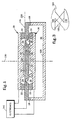
- Fig. 1 there is shown in cross section an embodiment of the invention adapted to register acceleration coaxial with an axis 230 extending upwardly through the drawing. For clarity, the vertical dimensions are greatly exaggerated.
- the apparatus is a three-plate capacitor in which top and bottom plates 20 and 30 respectively are formed of rigid silicon members that are bonded to an intermediate silicon frame 105 that contains a proof mass 110. Bonding, by means of standard anodic or thermal methods, is between frame 105 and glass borders 22 formed on the top and bottom plates 20 and 30 using standard glass deposition and etching techniques.
- Fig. 2 Differences between prior art three-plate capacitor arrangements and that of the present invention may be illustrated conveniently with respect to Fig. 2, showing frame 105 and proof mass 110 in simplified perspective.
- the same axis 230 is the Z axis in this drawing with corresponding X axis 210 and Y axis 220 which lie an the midplane of the proof mass and pass through its centroid.
- Proof mass 110 is surrounded by a gap 163 formed by anisotropic etching, illustratively EDP etching.
- An important distinction between prior art arrangements and the present invention is that of the layout of the flexures, or hinges, which couple proof mass 110 to frame 105.
- Y axis 220 it can be seen that there is a relatively large flexure 162 in the top plane at both the top and bottom of the drawing.
- On the bottom surface of proof mass 110 there is a pair of smaller flexures 164 disposed symmetrically about Y axis 220, each having half the width of flexure 162, so that the total stiffness of the flexures on the top and bottom surface is the same.
- On the lower portion of gap 163 on the opposite side of the proof mass there is a symmetric arrangement of corresponding flexures 162 and 164.
- the top and bottom of the arrangement symmetric about axis 220, but also it is symmetric about X axis 210 since there is a balance on the top and bottom of the drawing.
- flexures 164 and 162 that differs from the top and bottom sides in that the smaller flexures 164 are on the top surface and the larger one, 162, is on the bottom surface.
- axes 240 and 250 respectively, which extend along the diagonals of the square proof mass 110 midplane.
- axis 240 for example, there is a flexure 164 on the bottom surface of proof mass 110 on the left and a corresponding flexure 164 on the top surface on the right. This would induce a slight torque about axis 240 but that is balanced by corresponding flexures 162 on the bottom right and top left, respectively.
- flexure layout is not, of course, confined to a three-flexure per side arrangement and many other arrangements relative to widths, numbers and placement of the flexures will be evident to those skilled in the art.
- Flexures may be placed on the top and bottom surfaces, as shown, or in the midplane of the proof mass. The principle being followed in this embodiment is that of high symmetry about the transverse axes 210 and 220 together with the out of plane symmetry about the diagonal axes 240 and 250.
- Fig. 4A, 4B and 4C Alternative forms of proof mass 110 are illustrated in Fig. 4A, 4B and 4C.
- Etching of square corners in silicon is known to those skilled in the art to be possible by various techniques disclosed in the literature, such as "Corner Undercutting in Anisotropically Etched Contours", by M.M. Abou-Zaid, in Journal of the Electrochemical Society, Solid State Science and Technology, Sept. 1984, page 2138.
- Some expense can be saved by an arrangement such as that in Fig. 4A, in which the corners are permitted to be "faceted" or non-square.
- Fig. 4B has inside corners, which are square, as well as outside corners and has a longer “lever arm” for the hinges than for the capacitor which would be in the central portion. This may be useful for closed-loop applications.
- Fig. 4C shows a 12 sided layout that follows the contours that naturally result from differential etching. It is approximately circular, which aids in preserving the symmetry of the proof mass about the acceleration axis.
- the 4C embodiment would preferably have springs on four sides, for ease in fabricating consistent hinges of uniform length in the gap between the proof mass and the frame.
- ⁇ 100> oriented silicon was the starting material, with the geometry laid out so that the edges are along the ⁇ 110> directions. Anisotropic etching does not proceed at the same rate in the different crystal planes.
- the flexures 162 and 164 are fabricated by masking and boron doping both top and bottom surfaces of a silicon wafer illustratively 10 mils (about 0.25 in thickness such that the limit of 6xl019 boron atoms per cm3 is reached at the depth corresponding to the desired flexure thickness, illustratively 2 ⁇ m.
- the boron layers, in the top and bottom surfaces serve as etch stops for a standard anisotropic etchant, illustratively ethylenediamine pyrocatohol (EDP), so that when gap 163 is etched, the gap is opened until the boron layer is reached which serves as an etch stop in those areas where it exists and the etchant opens the apertures around the gap 163.
- a standard anisotropic etchant illustratively ethylenediamine pyrocatohol (EDP)
- EDP ethylenediamine pyrocatohol
- the wafer is etched from both top and bottom at the same time by immersing in a fluid bath.
- FIG. 1 the cross section is taken through the Y/Z plane showing two of flexures 162 at the top of proof mass 110.
- Apertures 24 in the top plate 20 and 26 in bottom plate 30 have been opened by any convenient etching method to sharply define the area of the variable capacitors formed by plates 20 and 30 and the proof mass 110 and also to reduce parasitic capacitance.
- gas will be forced out of the inter-plate chambers 32 and 34 into these apertures and into other apertures described below.
- the thickness of bonding glass 22 is relatively large compared with the capacitor gap and the horizontal dimension of the bonding glass 22 is relatively small compared with the width of mesa 31.
- the width of mesas 31 and 33 was about. 0.150 inch (about 3.8 mm) and the width of the glass 22 was about 0.010 inch (about 0.25 mm).
- the entire arrangement will be enclosed in a hermetically sealed enclosure having a pressure chosen for convenient damping and having a gas volume communicating with apertures 24 and 26 far in excess of the volume of capacitance chambers 32 and 34 plus the apertures 24 and 26.
- Insulating travel stops 72 are shown as being located at various locations on mesas 31 and 33 in order to prevent the proof mass from coming in contact with either mesa. These stops are illustratively glass coated in order to prevent electrical short circuits when the proof mass touches them and have illustrative dimensions of 0.005 inch (about 0.13 mm) in width and 0.4 ⁇ m in height, with a glass layer of 0.5 ⁇ m in thickness for insulation.
- the distance between capacitor plates may be controlled conveniently by the thickness of layer 22, so that the nominal capacitance, and thus the sensitivity of the sensor, may be altered without affecting the proof mass.
- the squeeze film damping phenomenon is used to control the frequency response of the proof mass.
- a sample channel or passageway is shown that serves to provide a reservoir to hold displaced gas that is squeezed out from the volume between the plates, denoted by the numeral 42. This channel will be part of a network covering surfaces 58 and 52. As chamber 34 contracts, gas is forced into these reservoirs.
- the total volume of the gas reservoirs should be considerably greater than the change in volume of gas chamber 34 so that there will be only a small increase in pressure in the reservoirs.
- the ratio is about 10 to 1 or greater and the channels have a width of 0.005" (about 0.13 mm) and a depth of 12 ⁇ m.
- Channels 42 are formed by any of the standard silicon processing techniques, such as ion milling or reactive ion etching. Since the passageways are relatively shallow, little additional surface is removed beyond that associated with their width in spite of the non-vertical walls that result from a wet etch process, as illustrated in the figure. In contrast, if the passageways are formed in the proof mass, its much greater thickness (typically .01”) (about 0.25 mm) requires deep trenches in order to form the through holes, thereby removing appreciable mass and surface area. Thus, the surface area effectively available for the capacitor is much reduced, and for a given capacitance the area of the capacitor itself must be larger.
- upper plate 20, lower plate 30 and frame 105 is supported by a three-dimensional lower frame 120 having a generally U-shaped cross section. It is connected to frame 105 by glass joints 28.
- An advantage of this method is that the thermal effects of heat conduction or loss to the outside world are entered symmetrically relative to the upper and lower plates. If the device were mounted on lower plate 30, for example, that would usually be at a different temperature from upper plate 20 with consequent thermal stresses and distortion and different temperatures experienced by the glass dielectric capacitors.
- the capacitance of the upper and lower capacitors is set by the gap between the proof mass and the surfaces of the top and bottom plates.
- This gap illustratively 2 microns, is determined both by the thickness of glass layers 22 which are deposited across the surface of the wafers and etched away except in predetermined areas and by the heights of mesas 31 and 33. Consequently, the gap can be controlled simply by changing the thickness of glass layer 22, in contrast to other art wherein the gap is set by removing material from the face of the proof mass.
- the network of damping passageways have minimal impact on the surface areas 52 and 58, and therefore on the capacitance , and being located on the plates 20 and 30 rather than on the proof mass 110 have no effect on the maximum detectable acceleration G max .
- the full scale range can be controlled independently by selecting the thickness of the proof mass and by controlling the numbers and the thicknesses of flexures 162 and 164 and their lengths and widths.
- flexures 162 and 164 had a thickness of 2.5 ⁇ m and respective widths of 0.066" (about 1.7 mm) and 0.033" (about 0.84) for gap spacing 163 of 0.010" (about 0.25 mm) and a proof mass 110 having a thickness of 0.010" (about 0.25 mm) and a mass of 7 milligrams. Since no material is removed from the proof mass to create the damping passageways in this invention, G max is independent of damping characteristics. Further, since the sensitivity is proportional to the ratio of the nominal capacitance to G max , two of the three parameters, sensitivity, capacitance and G max can be selected independently with the damping characteristics being virtually independent of these. This is in contrast to prior art designs wherein these parameters are all closely linked together and compromised because of the extensive sculpturing of the proof mass.
- the top and bottom silicon slabs 20 and 30 having a nominal thickness of 0.050" (about 1.3 mm) have within them top and bottom mesas referred to by the numerals 33 and 31, respectively.
- These mesas are formed by repeated oxidation of the areas that will be gas plenums 24 and 26 and that will contain the glass spacers 22, followed by etching to remove the silicon dioxide formed in repeated oxidation.
- the result of this method is a desirable, tightly controlled mesa area surrounded by extremely smooth surface upon which the glass dielectric is deposited.
- An accelerometer constructed according to the invention with a generally circular cross section and having a nominal diameter of .150 inches (about 3.8 mm) and a gap thickness of 2 ⁇ m has demonstrated resolution to one part in ten thousand with a response frequency from 0 Hertz to an adjustable upper limit of several hundred Hertz using an open loop configuration.
- a closed loop configuration would result in even better performance.
- the electronic portion of the apparatus is illustrated schematically in box 310. This box contains straight forward circuits which may apply forcing voltages to the electrodes for closed loop operation and also to sense capacitance by monitoring the unbalance of the high frequency bridge circuit of which the three-plate capacitor forms a part.
- a signal proportional to the external acceleration is derived from the forcing voltages required to return the proof mass to its null position.
- the restoring torques due to hinge deflections must overcome the electrostatic torques experienced by a proof mass that is not parallel to the plane defined by the surface of either mesa.
- the condition derived from the spring constant on the restoring voltages is that the voltage required to bring the proof mass back from contact with the travel stops, V null , be greater than the maximum voltage times a numerical factor, N; i.e., V null > N*V t , where N is of the order one, typically between 1/2 and 2 depending on the geometry and stiffness of the hinges and the shape of the proof mass, and V t is the maximum voltage available to be applied to the capacitor plates.
- N will depend on the shape of the proof mass and the location and stiffness of the hinges and may readily be calculated by those skilled in the art using the condition that the spring constant be able to overcome the electrical torque produced by misaligned capacitor plates. Small values of N are associated with a geometry in which the capacitor area is smaller than the proof mass, so that the torque exerted by the flexures has a larger lever arm than the electrostatic torque.
- G bottom /N2 G max
- G max the maximum acceleration that can be measured with the instrument
- G bottom the acceleration that will drive the proof mass in contact with the travel stops.
- Closed-loop accelerometers readily can be designed which will satisfy this stability constraint, which, when allowing for the numerical range given above, becomes G bottom /4 ⁇ G max ⁇ 4G bottom .
- the art customarily considers that the stiffness of the hinges in closed-loop accelerometers is not important. It can be seen, however, that the flexures may not be too soft and that there is a constraint on the sensitivity of the device.
- the sensitivity is close to the nominal capacitance divided by the acceleration that will force the proof mass down to the stops (about 3pf/G with this technology).
- the maximum acceleration that can be measured may be only one quarter of the acceleration that one would think of as the maximum.
- FIG. 3 there is shown an alternative layout for the flexures.
- this drawing which is a plan view of a portion of frame 105 and proof mass 110
- two diagonal flexures both referred to by the numeral 165, crossing gap 163.
- the angle of these flexures with the straight edges of frame 105 and proof mass 110 and their width and length is such that the right hand edge of the upper flexure 165 intersects proof mass 110 to the left of the point where the left hand edge of the same flexure intersects frame 105.
- the lower flexure has a similar displacement condition. Under these conditions, a wet etch in EDP will selectively undercut both Boron doped flexures leaving a gap in the space between them.
Landscapes
- Physics & Mathematics (AREA)
- General Physics & Mathematics (AREA)
- Pressure Sensors (AREA)
- Switches Operated By Changes In Physical Conditions (AREA)
Applications Claiming Priority (2)
| Application Number | Priority Date | Filing Date | Title |
|---|---|---|---|
| US317238 | 1989-02-28 | ||
| US07/317,238 US4930043A (en) | 1989-02-28 | 1989-02-28 | Closed-loop capacitive accelerometer with spring constraint |
Publications (3)
| Publication Number | Publication Date |
|---|---|
| EP0386464A2 true EP0386464A2 (fr) | 1990-09-12 |
| EP0386464A3 EP0386464A3 (fr) | 1992-03-25 |
| EP0386464B1 EP0386464B1 (fr) | 1994-07-13 |
Family
ID=23232746
Family Applications (1)
| Application Number | Title | Priority Date | Filing Date |
|---|---|---|---|
| EP90102092A Expired - Lifetime EP0386464B1 (fr) | 1989-02-28 | 1990-02-02 | Accéléromètre capacitif à compensationn d'inertie et force de rappel de ressort prédéterminée |
Country Status (7)
| Country | Link |
|---|---|
| US (1) | US4930043A (fr) |
| EP (1) | EP0386464B1 (fr) |
| JP (1) | JPH02271260A (fr) |
| BR (1) | BR9000843A (fr) |
| CA (1) | CA2010369A1 (fr) |
| DE (1) | DE69010525T2 (fr) |
| IL (1) | IL93549A (fr) |
Cited By (2)
| Publication number | Priority date | Publication date | Assignee | Title |
|---|---|---|---|---|
| EP0754953A1 (fr) | 1995-07-21 | 1997-01-22 | Commissariat A L'energie Atomique | Procédé de fabrication d'une structure avec une couche utile maintenue à distance d'un substrat par des butées, et de désolidarisation d'une telle couche |
| WO1997045703A1 (fr) * | 1996-05-29 | 1997-12-04 | Ruslanov, Alexandr Semenovich | Procede permettant de determiner la position d'un objet mobile et dispositif de mise en oeuvre de ce procede |
Families Citing this family (70)
| Publication number | Priority date | Publication date | Assignee | Title |
|---|---|---|---|---|
| US5326726A (en) * | 1990-08-17 | 1994-07-05 | Analog Devices, Inc. | Method for fabricating monolithic chip containing integrated circuitry and suspended microstructure |
| EP0543901B1 (fr) * | 1990-08-17 | 1995-10-04 | Analog Devices, Inc. | Accelerometre monolithique |
| US5314572A (en) * | 1990-08-17 | 1994-05-24 | Analog Devices, Inc. | Method for fabricating microstructures |
| US5417111A (en) | 1990-08-17 | 1995-05-23 | Analog Devices, Inc. | Monolithic chip containing integrated circuitry and suspended microstructure |
| US5620931A (en) * | 1990-08-17 | 1997-04-15 | Analog Devices, Inc. | Methods for fabricating monolithic device containing circuitry and suspended microstructure |
| US5069071A (en) * | 1990-08-27 | 1991-12-03 | United Technologies Corporation | Vibration monitoring in the frequency domain with a capacitive accelerometer |
| FR2687777B1 (fr) * | 1992-02-20 | 1994-05-20 | Sextant Avionique | Micro-capteur capacitif a faible capacite parasite et procede de fabrication. |
| US5333504A (en) * | 1992-09-01 | 1994-08-02 | Rosemount Inc. | High overpressure low range pressure sensor |
| FR2697090B1 (fr) * | 1992-10-21 | 1994-12-30 | Suisse Electronique Micro Cent | Dispositif de mesure d'une force. |
| EP0590658A1 (fr) * | 1992-10-02 | 1994-04-06 | CSEM, Centre Suisse d'Electronique et de Microtechnique S.A. | Dispositif de mesure d'une force |
| FR2701561B1 (fr) * | 1993-02-10 | 1995-05-05 | Sextant Avionique | Micro-capteur capacitif et procédé de découpe. |
| US6109114A (en) * | 1993-08-16 | 2000-08-29 | California Institute Of Technology | Caging, calibration, characterization and compensation of microstructural transducers |
| DE4332843C2 (de) * | 1993-09-27 | 1997-04-24 | Siemens Ag | Verfahren zur Herstellung einer mikromechanischen Vorrichtung und mikromechanische Vorrichtung |
| FR2710741B1 (fr) * | 1993-09-30 | 1995-10-27 | Commissariat Energie Atomique | Capteur électronique destiné à la caractérisation de grandeurs physiques et procédé de réalisation d'un tel capteur. |
| US5369057A (en) * | 1993-12-21 | 1994-11-29 | Delco Electronics Corporation | Method of making and sealing a semiconductor device having an air path therethrough |
| JP3435844B2 (ja) * | 1994-03-07 | 2003-08-11 | 株式会社デンソー | 半導体加速度センサ及びその製造方法 |
| US5604313A (en) * | 1994-11-23 | 1997-02-18 | Tokyo Gas Co., Ltd. | Varying apparent mass accelerometer |
| US5726480A (en) * | 1995-01-27 | 1998-03-10 | The Regents Of The University Of California | Etchants for use in micromachining of CMOS Microaccelerometers and microelectromechanical devices and method of making the same |
| FR2734641B1 (fr) * | 1995-05-24 | 1997-08-14 | Sextant Avionique | Accelerometre electromagnetique |
| RU2107301C1 (ru) * | 1996-06-03 | 1998-03-20 | Акционерное общество "Раменское приборостроительное конструкторское бюро" | Компенсационный акселерометр |
| US6303986B1 (en) | 1998-07-29 | 2001-10-16 | Silicon Light Machines | Method of and apparatus for sealing an hermetic lid to a semiconductor die |
| US6872984B1 (en) | 1998-07-29 | 2005-03-29 | Silicon Light Machines Corporation | Method of sealing a hermetic lid to a semiconductor die at an angle |
| US6956878B1 (en) | 2000-02-07 | 2005-10-18 | Silicon Light Machines Corporation | Method and apparatus for reducing laser speckle using polarization averaging |
| US7177081B2 (en) | 2001-03-08 | 2007-02-13 | Silicon Light Machines Corporation | High contrast grating light valve type device |
| US6707591B2 (en) | 2001-04-10 | 2004-03-16 | Silicon Light Machines | Angled illumination for a single order light modulator based projection system |
| US6865346B1 (en) | 2001-06-05 | 2005-03-08 | Silicon Light Machines Corporation | Fiber optic transceiver |
| US6782205B2 (en) | 2001-06-25 | 2004-08-24 | Silicon Light Machines | Method and apparatus for dynamic equalization in wavelength division multiplexing |
| US6747781B2 (en) | 2001-06-25 | 2004-06-08 | Silicon Light Machines, Inc. | Method, apparatus, and diffuser for reducing laser speckle |
| US6829092B2 (en) | 2001-08-15 | 2004-12-07 | Silicon Light Machines, Inc. | Blazed grating light valve |
| US6930364B2 (en) * | 2001-09-13 | 2005-08-16 | Silicon Light Machines Corporation | Microelectronic mechanical system and methods |
| US6956995B1 (en) | 2001-11-09 | 2005-10-18 | Silicon Light Machines Corporation | Optical communication arrangement |
| US6800238B1 (en) | 2002-01-15 | 2004-10-05 | Silicon Light Machines, Inc. | Method for domain patterning in low coercive field ferroelectrics |
| US6728023B1 (en) | 2002-05-28 | 2004-04-27 | Silicon Light Machines | Optical device arrays with optimized image resolution |
| US6767751B2 (en) * | 2002-05-28 | 2004-07-27 | Silicon Light Machines, Inc. | Integrated driver process flow |
| US7054515B1 (en) | 2002-05-30 | 2006-05-30 | Silicon Light Machines Corporation | Diffractive light modulator-based dynamic equalizer with integrated spectral monitor |
| US6822797B1 (en) | 2002-05-31 | 2004-11-23 | Silicon Light Machines, Inc. | Light modulator structure for producing high-contrast operation using zero-order light |
| US6862795B2 (en) * | 2002-06-17 | 2005-03-08 | Vty Holding Oy | Method of manufacturing of a monolithic silicon acceleration sensor |
| US6829937B2 (en) | 2002-06-17 | 2004-12-14 | Vti Holding Oy | Monolithic silicon acceleration sensor |
| US6829258B1 (en) | 2002-06-26 | 2004-12-07 | Silicon Light Machines, Inc. | Rapidly tunable external cavity laser |
| US6908201B2 (en) | 2002-06-28 | 2005-06-21 | Silicon Light Machines Corporation | Micro-support structures |
| US6813059B2 (en) | 2002-06-28 | 2004-11-02 | Silicon Light Machines, Inc. | Reduced formation of asperities in contact micro-structures |
| US6714337B1 (en) | 2002-06-28 | 2004-03-30 | Silicon Light Machines | Method and device for modulating a light beam and having an improved gamma response |
| US6801354B1 (en) | 2002-08-20 | 2004-10-05 | Silicon Light Machines, Inc. | 2-D diffraction grating for substantially eliminating polarization dependent losses |
| US7057795B2 (en) | 2002-08-20 | 2006-06-06 | Silicon Light Machines Corporation | Micro-structures with individually addressable ribbon pairs |
| US6712480B1 (en) | 2002-09-27 | 2004-03-30 | Silicon Light Machines | Controlled curvature of stressed micro-structures |
| US6928207B1 (en) | 2002-12-12 | 2005-08-09 | Silicon Light Machines Corporation | Apparatus for selectively blocking WDM channels |
| US7057819B1 (en) | 2002-12-17 | 2006-06-06 | Silicon Light Machines Corporation | High contrast tilting ribbon blazed grating |
| US6987600B1 (en) | 2002-12-17 | 2006-01-17 | Silicon Light Machines Corporation | Arbitrary phase profile for better equalization in dynamic gain equalizer |
| US6934070B1 (en) | 2002-12-18 | 2005-08-23 | Silicon Light Machines Corporation | Chirped optical MEM device |
| US6927891B1 (en) | 2002-12-23 | 2005-08-09 | Silicon Light Machines Corporation | Tilt-able grating plane for improved crosstalk in 1×N blaze switches |
| US7068372B1 (en) | 2003-01-28 | 2006-06-27 | Silicon Light Machines Corporation | MEMS interferometer-based reconfigurable optical add-and-drop multiplexor |
| US7286764B1 (en) | 2003-02-03 | 2007-10-23 | Silicon Light Machines Corporation | Reconfigurable modulator-based optical add-and-drop multiplexer |
| US6947613B1 (en) | 2003-02-11 | 2005-09-20 | Silicon Light Machines Corporation | Wavelength selective switch and equalizer |
| US6922272B1 (en) | 2003-02-14 | 2005-07-26 | Silicon Light Machines Corporation | Method and apparatus for leveling thermal stress variations in multi-layer MEMS devices |
| US6829077B1 (en) | 2003-02-28 | 2004-12-07 | Silicon Light Machines, Inc. | Diffractive light modulator with dynamically rotatable diffraction plane |
| US6806997B1 (en) | 2003-02-28 | 2004-10-19 | Silicon Light Machines, Inc. | Patterned diffractive light modulator ribbon for PDL reduction |
| US7027202B1 (en) | 2003-02-28 | 2006-04-11 | Silicon Light Machines Corp | Silicon substrate as a light modulator sacrificial layer |
| US6922273B1 (en) | 2003-02-28 | 2005-07-26 | Silicon Light Machines Corporation | PDL mitigation structure for diffractive MEMS and gratings |
| US7391973B1 (en) | 2003-02-28 | 2008-06-24 | Silicon Light Machines Corporation | Two-stage gain equalizer |
| US7042611B1 (en) | 2003-03-03 | 2006-05-09 | Silicon Light Machines Corporation | Pre-deflected bias ribbons |
| US7121141B2 (en) * | 2005-01-28 | 2006-10-17 | Freescale Semiconductor, Inc. | Z-axis accelerometer with at least two gap sizes and travel stops disposed outside an active capacitor area |
| US7490519B2 (en) * | 2005-09-30 | 2009-02-17 | General Electric Company | System and method for sensing differential pressure |
| US20070163346A1 (en) * | 2006-01-18 | 2007-07-19 | Honeywell International Inc. | Frequency shifting of rotational harmonics in mems devices |
| ITTO20070033A1 (it) * | 2007-01-19 | 2008-07-20 | St Microelectronics Srl | Dispositivo microelettromeccanico ad asse z con struttura di arresto perfezionata |
| DE102008042366A1 (de) * | 2008-09-25 | 2010-04-01 | Robert Bosch Gmbh | Sensor und Verfahren zur Herstellung eines Sensors |
| US8322216B2 (en) * | 2009-09-22 | 2012-12-04 | Duli Yu | Micromachined accelerometer with monolithic electrodes and method of making the same |
| CN102435780B (zh) * | 2011-11-22 | 2013-07-17 | 中国人民解放军国防科学技术大学 | 一种单片三轴微机械加速度计 |
| US9134337B2 (en) * | 2012-12-17 | 2015-09-15 | Maxim Integrated Products, Inc. | Microelectromechanical z-axis out-of-plane stopper |
| US9752900B2 (en) | 2015-07-10 | 2017-09-05 | Wyrobek International, Inc. | Multi-plate capacitive transducer |
| CN106289334A (zh) * | 2016-08-02 | 2017-01-04 | 上海芯赫科技有限公司 | 一种具有自检测功能的电容式复合传感器及其制造方法 |
Family Cites Families (9)
| Publication number | Priority date | Publication date | Assignee | Title |
|---|---|---|---|---|
| US4244225A (en) * | 1979-06-08 | 1981-01-13 | Itt Industries, Inc. | Mechanical resonator arrangements |
| GB2130373B (en) * | 1982-11-17 | 1986-12-31 | Stc Plc | Accelerometer device |
| GB2130372A (en) * | 1982-11-17 | 1984-05-31 | Stc Plc | Accelerometer device |
| US4699006A (en) * | 1984-03-19 | 1987-10-13 | The Charles Stark Draper Laboratory, Inc. | Vibratory digital integrating accelerometer |
| US4574327A (en) * | 1984-05-18 | 1986-03-04 | Becton, Dickinson And Company | Capacitive transducer |
| US4609968A (en) * | 1984-05-18 | 1986-09-02 | Becton, Dickinson And Company | Glass inlays for use in bonding semiconductor wafers |
| JPS6117959A (ja) * | 1984-07-05 | 1986-01-25 | Japan Aviation Electronics Ind Ltd | 加速度計 |
| US4679434A (en) * | 1985-07-25 | 1987-07-14 | Litton Systems, Inc. | Integrated force balanced accelerometer |
| DE3625411A1 (de) * | 1986-07-26 | 1988-02-04 | Messerschmitt Boelkow Blohm | Kapazitiver beschleunigungssensor |
-
1989
- 1989-02-28 US US07/317,238 patent/US4930043A/en not_active Expired - Fee Related
-
1990
- 1990-02-02 EP EP90102092A patent/EP0386464B1/fr not_active Expired - Lifetime
- 1990-02-02 DE DE69010525T patent/DE69010525T2/de not_active Expired - Fee Related
- 1990-02-19 CA CA002010369A patent/CA2010369A1/fr not_active Abandoned
- 1990-02-22 BR BR909000843A patent/BR9000843A/pt not_active Application Discontinuation
- 1990-02-27 IL IL93549A patent/IL93549A/xx not_active IP Right Cessation
- 1990-02-28 JP JP2049162A patent/JPH02271260A/ja active Pending
Cited By (3)
| Publication number | Priority date | Publication date | Assignee | Title |
|---|---|---|---|---|
| EP0754953A1 (fr) | 1995-07-21 | 1997-01-22 | Commissariat A L'energie Atomique | Procédé de fabrication d'une structure avec une couche utile maintenue à distance d'un substrat par des butées, et de désolidarisation d'une telle couche |
| US5750420A (en) * | 1995-07-21 | 1998-05-12 | Commissariat A L'energie Atomique | Method for manufacturing a structure with a useful layer held at a distance from a substrate by abutments, and for detaching such a layer |
| WO1997045703A1 (fr) * | 1996-05-29 | 1997-12-04 | Ruslanov, Alexandr Semenovich | Procede permettant de determiner la position d'un objet mobile et dispositif de mise en oeuvre de ce procede |
Also Published As
| Publication number | Publication date |
|---|---|
| US4930043A (en) | 1990-05-29 |
| CA2010369A1 (fr) | 1990-08-31 |
| DE69010525D1 (de) | 1994-08-18 |
| DE69010525T2 (de) | 1995-03-02 |
| IL93549A (en) | 1993-02-21 |
| JPH02271260A (ja) | 1990-11-06 |
| EP0386464B1 (fr) | 1994-07-13 |
| BR9000843A (pt) | 1991-02-05 |
| EP0386464A3 (fr) | 1992-03-25 |
Similar Documents
| Publication | Publication Date | Title |
|---|---|---|
| US4930043A (en) | Closed-loop capacitive accelerometer with spring constraint | |
| US4928203A (en) | Capacitive accelerometer with hinges on top and bottom surface | |
| EP0387518B1 (fr) | Accéléromètre capacitif avec amortissement et sensibilité indépendamment ajustables | |
| US5008774A (en) | Capacitive accelerometer with mid-plane proof mass | |
| US4574327A (en) | Capacitive transducer | |
| US6128953A (en) | Dynamical quantity sensor | |
| EP0490419B1 (fr) | Accéléromètre | |
| US6294400B1 (en) | Method for making micro-mechanical semiconductor accelerometer | |
| US5635739A (en) | Micromechanical angular accelerometer with auxiliary linear accelerometer | |
| US6935175B2 (en) | Capacitive pick-off and electrostatic rebalance accelerometer having equalized gas damping | |
| US6829937B2 (en) | Monolithic silicon acceleration sensor | |
| US5817942A (en) | Capacitive in-plane accelerometer | |
| EP3657178B1 (fr) | Accéléromètre | |
| FI81915B (fi) | Kapacitiv accelerationsgivare och foerfarande foer framstaellning daerav. | |
| US5780742A (en) | Mechanical resonance, silicon accelerometer | |
| US20010020726A1 (en) | Single crystal silicon sensor with high aspect ratio and curvilinear structures and associated method | |
| JPS6227666A (ja) | 加速度計 | |
| Lüdtke et al. | Laterally driven accelerometer fabricated in single crystalline silicon | |
| CN100565212C (zh) | 基于(111)硅的微机械加速度传感器及制造方法 | |
| US20230305036A1 (en) | Accelerometer element for detecting out-of-plane accelerations | |
| CA2213245C (fr) | Accelerometre au silicium a resonance mecanique | |
| Shoji et al. | Diode integrated capacitive accelerometer with reduced structural distortion | |
| EP4379396B1 (fr) | Optimisation de la conception de supports d'accéléromètre | |
| JP2512171B2 (ja) | 加速度検出器 | |
| JPH09178770A (ja) | 半導体加速度センサ |
Legal Events
| Date | Code | Title | Description |
|---|---|---|---|
| PUAI | Public reference made under article 153(3) epc to a published international application that has entered the european phase |
Free format text: ORIGINAL CODE: 0009012 |
|
| AK | Designated contracting states |
Kind code of ref document: A2 Designated state(s): DE FR GB IT NL SE |
|
| PUAL | Search report despatched |
Free format text: ORIGINAL CODE: 0009013 |
|
| AK | Designated contracting states |
Kind code of ref document: A3 Designated state(s): DE FR GB IT NL SE |
|
| 17P | Request for examination filed |
Effective date: 19920924 |
|
| 17Q | First examination report despatched |
Effective date: 19930107 |
|
| ITF | It: translation for a ep patent filed | ||
| GRAA | (expected) grant |
Free format text: ORIGINAL CODE: 0009210 |
|
| AK | Designated contracting states |
Kind code of ref document: B1 Designated state(s): DE FR GB IT NL SE |
|
| REF | Corresponds to: |
Ref document number: 69010525 Country of ref document: DE Date of ref document: 19940818 |
|
| ET | Fr: translation filed | ||
| EAL | Se: european patent in force in sweden |
Ref document number: 90102092.5 |
|
| PLBE | No opposition filed within time limit |
Free format text: ORIGINAL CODE: 0009261 |
|
| STAA | Information on the status of an ep patent application or granted ep patent |
Free format text: STATUS: NO OPPOSITION FILED WITHIN TIME LIMIT |
|
| 26N | No opposition filed | ||
| PGFP | Annual fee paid to national office [announced via postgrant information from national office to epo] |
Ref country code: SE Payment date: 19960117 Year of fee payment: 7 |
|
| PGFP | Annual fee paid to national office [announced via postgrant information from national office to epo] |
Ref country code: GB Payment date: 19960119 Year of fee payment: 7 |
|
| PGFP | Annual fee paid to national office [announced via postgrant information from national office to epo] |
Ref country code: NL Payment date: 19960123 Year of fee payment: 7 |
|
| PGFP | Annual fee paid to national office [announced via postgrant information from national office to epo] |
Ref country code: DE Payment date: 19960124 Year of fee payment: 7 |
|
| PGFP | Annual fee paid to national office [announced via postgrant information from national office to epo] |
Ref country code: FR Payment date: 19960201 Year of fee payment: 7 |
|
| PG25 | Lapsed in a contracting state [announced via postgrant information from national office to epo] |
Ref country code: GB Effective date: 19970202 |
|
| PG25 | Lapsed in a contracting state [announced via postgrant information from national office to epo] |
Ref country code: SE Effective date: 19970203 |
|
| PG25 | Lapsed in a contracting state [announced via postgrant information from national office to epo] |
Ref country code: NL Effective date: 19970901 |
|
| GBPC | Gb: european patent ceased through non-payment of renewal fee |
Effective date: 19970202 |
|
| PG25 | Lapsed in a contracting state [announced via postgrant information from national office to epo] |
Ref country code: FR Effective date: 19971030 |
|
| PG25 | Lapsed in a contracting state [announced via postgrant information from national office to epo] |
Ref country code: DE Effective date: 19971101 |
|
| EUG | Se: european patent has lapsed |
Ref document number: 90102092.5 |
|
| NLV4 | Nl: lapsed or anulled due to non-payment of the annual fee |
Effective date: 19970901 |
|
| REG | Reference to a national code |
Ref country code: FR Ref legal event code: ST |
|
| PG25 | Lapsed in a contracting state [announced via postgrant information from national office to epo] |
Ref country code: IT Free format text: LAPSE BECAUSE OF NON-PAYMENT OF DUE FEES;WARNING: LAPSES OF ITALIAN PATENTS WITH EFFECTIVE DATE BEFORE 2007 MAY HAVE OCCURRED AT ANY TIME BEFORE 2007. THE CORRECT EFFECTIVE DATE MAY BE DIFFERENT FROM THE ONE RECORDED. Effective date: 20050202 |