EP0387789A2 - Matrice de commutation à large bande pour égalisation de retard et élimination d'inversion - Google Patents
Matrice de commutation à large bande pour égalisation de retard et élimination d'inversion Download PDFInfo
- Publication number
- EP0387789A2 EP0387789A2 EP90104725A EP90104725A EP0387789A2 EP 0387789 A2 EP0387789 A2 EP 0387789A2 EP 90104725 A EP90104725 A EP 90104725A EP 90104725 A EP90104725 A EP 90104725A EP 0387789 A2 EP0387789 A2 EP 0387789A2
- Authority
- EP
- European Patent Office
- Prior art keywords
- input
- output
- switching
- column
- row
- Prior art date
- Legal status (The legal status is an assumption and is not a legal conclusion. Google has not performed a legal analysis and makes no representation as to the accuracy of the status listed.)
- Granted
Links
- 239000011159 matrix material Substances 0.000 title description 12
- 230000008030 elimination Effects 0.000 title 1
- 238000003379 elimination reaction Methods 0.000 title 1
- 230000001902 propagating effect Effects 0.000 claims description 7
- 230000001186 cumulative effect Effects 0.000 claims description 3
- 230000000295 complement effect Effects 0.000 claims 6
- 230000003334 potential effect Effects 0.000 claims 1
- 230000001934 delay Effects 0.000 description 5
- 238000003491 array Methods 0.000 description 2
- 230000015556 catabolic process Effects 0.000 description 2
- 238000006731 degradation reaction Methods 0.000 description 2
- 238000010586 diagram Methods 0.000 description 2
- 230000000694 effects Effects 0.000 description 2
- 230000003292 diminished effect Effects 0.000 description 1
- 238000005516 engineering process Methods 0.000 description 1
- 238000000034 method Methods 0.000 description 1
- 230000003287 optical effect Effects 0.000 description 1
Images

Classifications
-
- H—ELECTRICITY
- H04—ELECTRIC COMMUNICATION TECHNIQUE
- H04Q—SELECTING
- H04Q3/00—Selecting arrangements
- H04Q3/42—Circuit arrangements for indirect selecting controlled by common circuits, e.g. register controller, marker
- H04Q3/52—Circuit arrangements for indirect selecting controlled by common circuits, e.g. register controller, marker using static devices in switching stages, e.g. electronic switching arrangements
- H04Q3/521—Circuit arrangements for indirect selecting controlled by common circuits, e.g. register controller, marker using static devices in switching stages, e.g. electronic switching arrangements using semiconductors in the switching stages
Definitions
- This invention relates to electrical switching systems and, more particularly, to broadband switching arrays having compensating circuits for propagation delay and polarity inversion.
- the present invention provides a crosspoint switching array for connecting any one of a plurality of M input ports to any one of a plurality of N output ports.
- the array includes MXN crosspoint switching means arranged in M rows by N columns wherein each switching path has a known propagation delay and performs a series of inversion operations on an input signal propagating through the path. Delay equalization among all switching paths is accomplished by attaching a cascaded set of delay means to each of the M input ports via a first serial connecting means. The particular set of delay means for each input port is determined according to the propagation delay which already exists due to the array of MxN crosspoint switching means.
- the crosspoint switching array further includes inverter means.
- a second serial connecting means attaches a set of cascaded inverter means to each of the N output ports so that each switching path performs a common number of inversion operations on an input signal propagating through the respective path, thereby providing output signals with the same logical polarity .
- the delay means includes dummy selector means having a first input, a second input connected to a point of reference potential, and an output for selecting the digital signal present on the first input and inverting it before placing the inverted signal on said output.
- the array Since the delay from input to output in Figure 1 is a function of the path traversed by the signal, where the shortest path is from Row K to Output 1 and the longest path is from Row 1 to Output J, the array has the undesirable effect of having the inputs appear at the respective outputs with varying delays. Furthermore, the output logic polarity is non-uniform due to the even and odd numbers of stages present in the array. As a result, circuitry which receives and utilizes the output signals from the switching array of Figure 1 requires additional control circuitry to compensate for the variable delays and non-uniform output polarities.
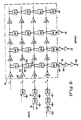
- Figure 2 shows a switching array according to the present invention having novel improvements to the above-mentioned matrix of Figure 1.
- the operation of the present invention will be discussed in relation to a 4x4 switching array.
- the array can be easily expanded to accomodate any matrix dimension.
- Configuration 10 includes sixteen crosspoint switching means arranged in a 4x4 matrix wherein each crosspoint switching means includes an inverter element serving as a buffer and a 2:1 selector element for selecting one of the two input signals and placing the selected signal on an output line.
- each crosspoint switching means includes an inverter element serving as a buffer and a 2:1 selector element for selecting one of the two input signals and placing the selected signal on an output line.
- the crosspoint switch located at the intersection of Row 2 and Column 1 has an inverter 21 having an input 213 connected to the output of a preceding inverter in the row (or in this case, to input port 2) and an output 214 connected to the input of a following inverter 22 in the row.
- the switch also has a selector S) having a first input 215 connected to the output of a preceding selector S11 in the column, a second input 216 connected to the output of inverter 21, and an output 217 connected to the first input of the next selector element S) in the column.
- This particular crosspoint switch operates in response to control signals applied to the selector 21 for selecting the digital signal present on either input 215 or input 216 and placing it on output 217.
- Each other crosspoint switch in array 10 operates in the same manner.
- Array 10 imposes variable delays on a propagating signal due to the different numbers of stages in each switching path, and also provides non-uniform output polarities resulting from the even and odd numbers of stages in the switching paths. As will be discussed next, delay equalization is accomplished by connecting dummy selectors SXX to the input ports, while uniform output polarities are achieved by connecting dummy inverters 30 to the output ports.
- the array 10 is modified by introducing an additional delay at the input end of each switching path in the array. This is accomplished by connecting a particular set of cascaded 2:1 dummy selector elements SXX, each having a known time delay, to each of the input ports of array 10. Since each switching path in array 10 has a known propagation delay, the amount of delay which needs to be added, and thus the number of dummy selector elements SXX, can easily be determined. Accordingly, an appropriate number of dummy selectors SXX are cascaded in series, if more than one is needed, and then connected to the input port.
- the dummy selectors SXX are identical in structure and function to those in the crosspoint switches of array 10.
- the control on selector SXX always selects the upper input 60 and places the selected signal on output 70.
- the other input 50 is grounded to prevent floating inputs.
- Dummy selector SXX simply imposes a time delay on a digital signal as it propagates through the dummy selector SXX from input line 60 to output line 70.
- the dummy selector SXX also performs an inversion operation on the selected signal.
- a set of one, two, and three cascaded dummy selectors SXX are connected to each of the input ports 2, 3, and 4, respectively, so that an input signal applied to each of these input ports will encounter a cumulative total of four selector elements, irrespective of the switching path, when the signal propagates through its designated path.
- the respective numbers of dummy selectors SXX and 2:1 crosspoint selector elements from array 10 in each switching path will obviously depend upon the particular path that is chosen.
- the output polarities are made non-inverting by connecting a cascaded set of dummy inverters 30 to each output port so that each switched signal experiences an even number of inversion operations while propagating through the signal's respective path of dummy selectors SXX, dummy inverters 30, and crosspoint selectors and inverters from the crosspoint switches of array 10.
- Each inverter 30 has an input 301 and an output 302 for providing a signal of opposite polarity to that of the signal entering input 301.
- the output from one inverter serves as the input to the following inverter in the series.
- the signal appearing at an output port of array 10, such as output port 1 is applied to input 301 of the first dummy inverter 30 in the series, while the output 303 from the last inverter in the series serves as the input to external circuitry which may be coupled to the matrix outputs.
Landscapes
- Engineering & Computer Science (AREA)
- Computer Networks & Wireless Communication (AREA)
- Electronic Switches (AREA)
- Use Of Switch Circuits For Exchanges And Methods Of Control Of Multiplex Exchanges (AREA)
- Data Exchanges In Wide-Area Networks (AREA)
Applications Claiming Priority (2)
| Application Number | Priority Date | Filing Date | Title |
|---|---|---|---|
| US07/324,848 US4970507A (en) | 1989-03-17 | 1989-03-17 | Broadband switching matrix for delay equalization and elimination of inversion |
| US324848 | 1989-03-17 |
Publications (3)
| Publication Number | Publication Date |
|---|---|
| EP0387789A2 true EP0387789A2 (fr) | 1990-09-19 |
| EP0387789A3 EP0387789A3 (fr) | 1992-05-13 |
| EP0387789B1 EP0387789B1 (fr) | 1994-06-15 |
Family
ID=23265372
Family Applications (1)
| Application Number | Title | Priority Date | Filing Date |
|---|---|---|---|
| EP90104725A Expired - Lifetime EP0387789B1 (fr) | 1989-03-17 | 1990-03-13 | Matrice de commutation à large bande pour égalisation de retard et élimination d'inversion |
Country Status (5)
| Country | Link |
|---|---|
| US (1) | US4970507A (fr) |
| EP (1) | EP0387789B1 (fr) |
| JP (1) | JPH02306795A (fr) |
| CA (1) | CA2011827A1 (fr) |
| DE (1) | DE69009807T2 (fr) |
Cited By (1)
| Publication number | Priority date | Publication date | Assignee | Title |
|---|---|---|---|---|
| US5857009A (en) * | 1996-01-18 | 1999-01-05 | Telefonaktiebolaget Lm Ericsson | Method and apparatus for propagation delay determination |
Families Citing this family (15)
| Publication number | Priority date | Publication date | Assignee | Title |
|---|---|---|---|---|
| US5049877A (en) * | 1989-03-17 | 1991-09-17 | Gte Laboratories Incorporated | Broadband switch matrix with non-linear cascading |
| CA2015809A1 (fr) * | 1989-05-04 | 1990-11-04 | Richard W. Sieber | Commutateur a large bande utilisant des points de croisement hors fonction pour etablir les trajets de commutation |
| US5465087A (en) * | 1989-05-04 | 1995-11-07 | Gte Laboratories Incorporated | Broadband switch |
| US5066868A (en) * | 1990-08-13 | 1991-11-19 | Thomson Consumer Electronics, Inc. | Apparatus for generating phase shifted clock signals |
| SE515177C2 (sv) * | 1992-06-01 | 2001-06-25 | Ericsson Telefon Ab L M | Kvadratisk väljararkitektur |
| JPH0621788A (ja) * | 1992-07-01 | 1994-01-28 | Mitsubishi Electric Corp | 半導体集積回路 |
| US5377182A (en) * | 1993-08-18 | 1994-12-27 | The United States Of America As Represented By The Administrator Of The National Aeronautics And Space Administration | Non-blocking crossbar permutation engine with constant routing latency |
| US5856746A (en) * | 1996-06-17 | 1999-01-05 | Sun Microsystems, Inc. | Logic speed-up by selecting true/false combinations with the slowest logic signal |
| US6636932B1 (en) | 1998-05-27 | 2003-10-21 | Micron Technology, Inc. | Crossbar switch and control for data networks switching |
| US7106728B1 (en) | 2000-05-01 | 2006-09-12 | Industrial Technology Research Institute | Switching by multistage interconnection of concentrators |
| US6591285B1 (en) | 2000-06-16 | 2003-07-08 | Shuo-Yen Robert Li | Running-sum adder networks determined by recursive construction of multi-stage networks |
| US7103059B2 (en) * | 2001-06-15 | 2006-09-05 | Industrial Technology Research Institute | Scalable 2-stage interconnections |
| US7609695B2 (en) * | 2001-06-15 | 2009-10-27 | Industrial Technology Research Institute | Optimizing switching element for minimal latency |
| US9712177B1 (en) * | 2016-01-08 | 2017-07-18 | Samsung Display Co., Ltd. | Fractional PLL using a linear PFD with adjustable delay |
| FR3100019B1 (fr) | 2019-08-23 | 2021-07-23 | Psa Automobiles Sa | Renfort pour corps creux |
Family Cites Families (5)
| Publication number | Priority date | Publication date | Assignee | Title |
|---|---|---|---|---|
| DE2944794C2 (de) * | 1979-11-06 | 1981-11-12 | Siemens AG, 1000 Berlin und 8000 München | Breitband-Koppelanordnung |
| US4771281A (en) * | 1984-02-13 | 1988-09-13 | Prime Computer, Inc. | Bit selection and routing apparatus and method |
| US4737670A (en) * | 1984-11-09 | 1988-04-12 | Lsi Logic Corporation | Delay control circuit |
| JPS62180607A (ja) * | 1986-02-04 | 1987-08-07 | Fujitsu Ltd | 半導体集積回路 |
| US4818988A (en) * | 1988-01-04 | 1989-04-04 | Gte Laboratories Incorporated | Crosspoint switching array |
-
1989
- 1989-03-17 US US07/324,848 patent/US4970507A/en not_active Expired - Lifetime
-
1990
- 1990-03-09 CA CA002011827A patent/CA2011827A1/fr not_active Abandoned
- 1990-03-13 DE DE69009807T patent/DE69009807T2/de not_active Expired - Fee Related
- 1990-03-13 EP EP90104725A patent/EP0387789B1/fr not_active Expired - Lifetime
- 1990-03-16 JP JP2064498A patent/JPH02306795A/ja active Pending
Cited By (1)
| Publication number | Priority date | Publication date | Assignee | Title |
|---|---|---|---|---|
| US5857009A (en) * | 1996-01-18 | 1999-01-05 | Telefonaktiebolaget Lm Ericsson | Method and apparatus for propagation delay determination |
Also Published As
| Publication number | Publication date |
|---|---|
| CA2011827A1 (fr) | 1990-09-17 |
| US4970507A (en) | 1990-11-13 |
| DE69009807T2 (de) | 1994-09-29 |
| EP0387789B1 (fr) | 1994-06-15 |
| DE69009807D1 (de) | 1994-07-21 |
| JPH02306795A (ja) | 1990-12-20 |
| EP0387789A3 (fr) | 1992-05-13 |
Similar Documents
| Publication | Publication Date | Title |
|---|---|---|
| EP0387789B1 (fr) | Matrice de commutation à large bande pour égalisation de retard et élimination d'inversion | |
| CA1318960C (fr) | Reseau de commutateurs | |
| EP0295001B1 (fr) | Montage de configuration en circuit intégré CMOS d'un arbre logique à entrance | |
| EP0386958B1 (fr) | Réseau de commutation étendu à deux barres | |
| EP0385661B1 (fr) | Réseaux de commutation optiques | |
| AU627761B2 (en) | Binary tree switching network | |
| KR890002782A (ko) | 데이타 처리 회로용 교차 메모리 | |
| US5604617A (en) | Telecommunications switching element | |
| JPS6039921A (ja) | プログラマブル論理アレー | |
| US5285202A (en) | Broadband switch using deactivated crosspoints for establishing switching paths | |
| US5049877A (en) | Broadband switch matrix with non-linear cascading | |
| US5047766A (en) | Broad band signal switching matrix | |
| EP0387788A2 (fr) | Matrice de commutateurs à large bande et à montage en cascade non linéaire | |
| US3215782A (en) | Switching systems employing co-ordinate switching arrangements of the cross-point type | |
| EP0397093B1 (fr) | Matrice de commutation spatiale à large bande utilisant une sensibilisation des parcours | |
| US4186277A (en) | Time division multiplex telecommunications switching network | |
| US5170160A (en) | Broadband tree switch architecture for reducing pulse width narrowing and power dissipation | |
| US6888825B1 (en) | Cross-connect with shared storage | |
| JPH0339439B2 (fr) | ||
| HK191895A (en) | Dual rail dilated switching networks | |
| JP2000214498A (ja) | 光スイッチ | |
| JP2001136551A (ja) | タイムスロット交換装置 | |
| GB2175109A (en) | Digital code detector circuits | |
| GB1433254A (en) | Digital telecommunications switching systems |
Legal Events
| Date | Code | Title | Description |
|---|---|---|---|
| PUAI | Public reference made under article 153(3) epc to a published international application that has entered the european phase |
Free format text: ORIGINAL CODE: 0009012 |
|
| AK | Designated contracting states |
Kind code of ref document: A2 Designated state(s): BE DE FR GB IT |
|
| PUAL | Search report despatched |
Free format text: ORIGINAL CODE: 0009013 |
|
| AK | Designated contracting states |
Kind code of ref document: A3 Designated state(s): BE DE FR GB IT |
|
| 17P | Request for examination filed |
Effective date: 19921112 |
|
| 17Q | First examination report despatched |
Effective date: 19930713 |
|
| GRAA | (expected) grant |
Free format text: ORIGINAL CODE: 0009210 |
|
| AK | Designated contracting states |
Kind code of ref document: B1 Designated state(s): BE DE FR GB IT |
|
| ET | Fr: translation filed | ||
| REF | Corresponds to: |
Ref document number: 69009807 Country of ref document: DE Date of ref document: 19940721 |
|
| ITF | It: translation for a ep patent filed | ||
| PGFP | Annual fee paid to national office [announced via postgrant information from national office to epo] |
Ref country code: GB Payment date: 19950302 Year of fee payment: 6 |
|
| PGFP | Annual fee paid to national office [announced via postgrant information from national office to epo] |
Ref country code: BE Payment date: 19950303 Year of fee payment: 6 |
|
| PGFP | Annual fee paid to national office [announced via postgrant information from national office to epo] |
Ref country code: FR Payment date: 19950309 Year of fee payment: 6 |
|
| PLBE | No opposition filed within time limit |
Free format text: ORIGINAL CODE: 0009261 |
|
| STAA | Information on the status of an ep patent application or granted ep patent |
Free format text: STATUS: NO OPPOSITION FILED WITHIN TIME LIMIT |
|
| PGFP | Annual fee paid to national office [announced via postgrant information from national office to epo] |
Ref country code: DE Payment date: 19950428 Year of fee payment: 6 |
|
| 26N | No opposition filed | ||
| PG25 | Lapsed in a contracting state [announced via postgrant information from national office to epo] |
Ref country code: GB Effective date: 19960313 |
|
| PG25 | Lapsed in a contracting state [announced via postgrant information from national office to epo] |
Ref country code: BE Effective date: 19960331 |
|
| BERE | Be: lapsed |
Owner name: GTE LABORATORIES INC. Effective date: 19960331 |
|
| GBPC | Gb: european patent ceased through non-payment of renewal fee |
Effective date: 19960313 |
|
| PG25 | Lapsed in a contracting state [announced via postgrant information from national office to epo] |
Ref country code: FR Effective date: 19961129 |
|
| PG25 | Lapsed in a contracting state [announced via postgrant information from national office to epo] |
Ref country code: DE Effective date: 19961203 |
|
| REG | Reference to a national code |
Ref country code: FR Ref legal event code: ST |
|
| PG25 | Lapsed in a contracting state [announced via postgrant information from national office to epo] |
Ref country code: IT Free format text: LAPSE BECAUSE OF NON-PAYMENT OF DUE FEES Effective date: 20050313 |