EP0388023B1 - Atomisches Kraftmikroskop mit nach Wahl auswechselbarer Flüssigkeitszelle - Google Patents
Atomisches Kraftmikroskop mit nach Wahl auswechselbarer Flüssigkeitszelle Download PDFInfo
- Publication number
- EP0388023B1 EP0388023B1 EP90301688A EP90301688A EP0388023B1 EP 0388023 B1 EP0388023 B1 EP 0388023B1 EP 90301688 A EP90301688 A EP 90301688A EP 90301688 A EP90301688 A EP 90301688A EP 0388023 B1 EP0388023 B1 EP 0388023B1
- Authority
- EP
- European Patent Office
- Prior art keywords
- probe
- sample
- atomic force
- force microscope
- microscope according
- Prior art date
- Legal status (The legal status is an assumption and is not a legal conclusion. Google has not performed a legal analysis and makes no representation as to the accuracy of the status listed.)
- Expired - Lifetime
Links
- 239000012530 fluid Substances 0.000 title claims description 37
- 239000000523 sample Substances 0.000 claims abstract description 191
- 230000003287 optical effect Effects 0.000 claims abstract description 5
- 238000001514 detection method Methods 0.000 claims abstract description 4
- 238000000034 method Methods 0.000 claims description 21
- 230000008569 process Effects 0.000 claims description 7
- XLYOFNOQVPJJNP-UHFFFAOYSA-N water Substances O XLYOFNOQVPJJNP-UHFFFAOYSA-N 0.000 claims description 5
- 230000005291 magnetic effect Effects 0.000 claims description 4
- 239000012780 transparent material Substances 0.000 claims description 2
- 238000003487 electrochemical reaction Methods 0.000 claims 2
- 230000008878 coupling Effects 0.000 claims 1
- 238000010168 coupling process Methods 0.000 claims 1
- 238000005859 coupling reaction Methods 0.000 claims 1
- 239000000758 substrate Substances 0.000 description 16
- 229910000831 Steel Inorganic materials 0.000 description 9
- 239000010959 steel Substances 0.000 description 9
- 230000009471 action Effects 0.000 description 7
- 239000000463 material Substances 0.000 description 7
- 238000013459 approach Methods 0.000 description 4
- 230000008859 change Effects 0.000 description 4
- 239000011248 coating agent Substances 0.000 description 4
- 238000000576 coating method Methods 0.000 description 4
- 239000006059 cover glass Substances 0.000 description 4
- 230000006378 damage Effects 0.000 description 4
- 230000008901 benefit Effects 0.000 description 3
- 239000010432 diamond Substances 0.000 description 3
- 229910003460 diamond Inorganic materials 0.000 description 3
- 230000007246 mechanism Effects 0.000 description 3
- 238000012876 topography Methods 0.000 description 3
- 230000003466 anti-cipated effect Effects 0.000 description 2
- 238000013461 design Methods 0.000 description 2
- 238000001704 evaporation Methods 0.000 description 2
- 230000008020 evaporation Effects 0.000 description 2
- 239000003302 ferromagnetic material Substances 0.000 description 2
- 230000001050 lubricating effect Effects 0.000 description 2
- 238000004377 microelectronic Methods 0.000 description 2
- 238000000386 microscopy Methods 0.000 description 2
- 239000004033 plastic Substances 0.000 description 2
- 230000000284 resting effect Effects 0.000 description 2
- 239000000126 substance Substances 0.000 description 2
- 230000005641 tunneling Effects 0.000 description 2
- 241001391944 Commicarpus scandens Species 0.000 description 1
- 229910001218 Gallium arsenide Inorganic materials 0.000 description 1
- 239000000853 adhesive Substances 0.000 description 1
- 230000001070 adhesive effect Effects 0.000 description 1
- 230000002411 adverse Effects 0.000 description 1
- 238000010420 art technique Methods 0.000 description 1
- 230000007797 corrosion Effects 0.000 description 1
- 238000005260 corrosion Methods 0.000 description 1
- 239000008367 deionised water Substances 0.000 description 1
- 238000011161 development Methods 0.000 description 1
- 238000001035 drying Methods 0.000 description 1
- 230000000694 effects Effects 0.000 description 1
- 238000005516 engineering process Methods 0.000 description 1
- 230000005294 ferromagnetic effect Effects 0.000 description 1
- 239000000835 fiber Substances 0.000 description 1
- 239000011521 glass Substances 0.000 description 1
- 239000003292 glue Substances 0.000 description 1
- 230000003760 hair shine Effects 0.000 description 1
- 238000003384 imaging method Methods 0.000 description 1
- 238000011065 in-situ storage Methods 0.000 description 1
- 238000003780 insertion Methods 0.000 description 1
- 230000037431 insertion Effects 0.000 description 1
- 238000009434 installation Methods 0.000 description 1
- 239000007788 liquid Substances 0.000 description 1
- 238000004519 manufacturing process Methods 0.000 description 1
- 239000002184 metal Substances 0.000 description 1
- 238000007747 plating Methods 0.000 description 1
- 239000004417 polycarbonate Substances 0.000 description 1
- 229920000515 polycarbonate Polymers 0.000 description 1
- 239000010453 quartz Substances 0.000 description 1
- 238000004064 recycling Methods 0.000 description 1
- 230000009467 reduction Effects 0.000 description 1
- 239000004065 semiconductor Substances 0.000 description 1
- 230000035939 shock Effects 0.000 description 1
- VYPSYNLAJGMNEJ-UHFFFAOYSA-N silicon dioxide Inorganic materials O=[Si]=O VYPSYNLAJGMNEJ-UHFFFAOYSA-N 0.000 description 1
- 210000004872 soft tissue Anatomy 0.000 description 1
- 238000012549 training Methods 0.000 description 1
Images



Classifications
-
- G—PHYSICS
- G01—MEASURING; TESTING
- G01Q—SCANNING-PROBE TECHNIQUES OR APPARATUS; APPLICATIONS OF SCANNING-PROBE TECHNIQUES, e.g. SCANNING PROBE MICROSCOPY [SPM]
- G01Q60/00—Particular types of SPM [Scanning Probe Microscopy] or microscopes; Essential components thereof
- G01Q60/24—AFM [Atomic Force Microscopy] or apparatus therefor, e.g. AFM probes
- G01Q60/38—Probes, their manufacture, or their related instrumentation, e.g. holders
-
- B—PERFORMING OPERATIONS; TRANSPORTING
- B82—NANOTECHNOLOGY
- B82Y—SPECIFIC USES OR APPLICATIONS OF NANOSTRUCTURES; MEASUREMENT OR ANALYSIS OF NANOSTRUCTURES; MANUFACTURE OR TREATMENT OF NANOSTRUCTURES
- B82Y35/00—Methods or apparatus for measurement or analysis of nanostructures
-
- G—PHYSICS
- G01—MEASURING; TESTING
- G01Q—SCANNING-PROBE TECHNIQUES OR APPARATUS; APPLICATIONS OF SCANNING-PROBE TECHNIQUES, e.g. SCANNING PROBE MICROSCOPY [SPM]
- G01Q30/00—Auxiliary means serving to assist or improve the scanning probe techniques or apparatus, e.g. display or data processing devices
- G01Q30/02—Non-SPM analysing devices, e.g. SEM [Scanning Electron Microscope], spectrometer or optical microscope
- G01Q30/025—Optical microscopes coupled with SPM
-
- G—PHYSICS
- G01—MEASURING; TESTING
- G01Q—SCANNING-PROBE TECHNIQUES OR APPARATUS; APPLICATIONS OF SCANNING-PROBE TECHNIQUES, e.g. SCANNING PROBE MICROSCOPY [SPM]
- G01Q30/00—Auxiliary means serving to assist or improve the scanning probe techniques or apparatus, e.g. display or data processing devices
- G01Q30/08—Means for establishing or regulating a desired environmental condition within a sample chamber
- G01Q30/12—Fluid environment
- G01Q30/14—Liquid environment
-
- G—PHYSICS
- G01—MEASURING; TESTING
- G01Q—SCANNING-PROBE TECHNIQUES OR APPARATUS; APPLICATIONS OF SCANNING-PROBE TECHNIQUES, e.g. SCANNING PROBE MICROSCOPY [SPM]
- G01Q70/00—General aspects of SPM probes, their manufacture or their related instrumentation, insofar as they are not specially adapted to a single SPM technique covered by group G01Q60/00
- G01Q70/02—Probe holders
-
- G—PHYSICS
- G01—MEASURING; TESTING
- G01Q—SCANNING-PROBE TECHNIQUES OR APPARATUS; APPLICATIONS OF SCANNING-PROBE TECHNIQUES, e.g. SCANNING PROBE MICROSCOPY [SPM]
- G01Q70/00—General aspects of SPM probes, their manufacture or their related instrumentation, insofar as they are not specially adapted to a single SPM technique covered by group G01Q60/00
- G01Q70/02—Probe holders
- G01Q70/04—Probe holders with compensation for temperature or vibration induced errors
-
- Y—GENERAL TAGGING OF NEW TECHNOLOGICAL DEVELOPMENTS; GENERAL TAGGING OF CROSS-SECTIONAL TECHNOLOGIES SPANNING OVER SEVERAL SECTIONS OF THE IPC; TECHNICAL SUBJECTS COVERED BY FORMER USPC CROSS-REFERENCE ART COLLECTIONS [XRACs] AND DIGESTS
- Y10—TECHNICAL SUBJECTS COVERED BY FORMER USPC
- Y10S—TECHNICAL SUBJECTS COVERED BY FORMER USPC CROSS-REFERENCE ART COLLECTIONS [XRACs] AND DIGESTS
- Y10S977/00—Nanotechnology
- Y10S977/84—Manufacture, treatment, or detection of nanostructure
- Y10S977/849—Manufacture, treatment, or detection of nanostructure with scanning probe
- Y10S977/86—Scanning probe structure
- Y10S977/863—Atomic force probe
-
- Y—GENERAL TAGGING OF NEW TECHNOLOGICAL DEVELOPMENTS; GENERAL TAGGING OF CROSS-SECTIONAL TECHNOLOGIES SPANNING OVER SEVERAL SECTIONS OF THE IPC; TECHNICAL SUBJECTS COVERED BY FORMER USPC CROSS-REFERENCE ART COLLECTIONS [XRACs] AND DIGESTS
- Y10—TECHNICAL SUBJECTS COVERED BY FORMER USPC
- Y10S—TECHNICAL SUBJECTS COVERED BY FORMER USPC CROSS-REFERENCE ART COLLECTIONS [XRACs] AND DIGESTS
- Y10S977/00—Nanotechnology
- Y10S977/84—Manufacture, treatment, or detection of nanostructure
- Y10S977/849—Manufacture, treatment, or detection of nanostructure with scanning probe
- Y10S977/86—Scanning probe structure
- Y10S977/868—Scanning probe structure with optical means
- Y10S977/87—Optical lever arm for reflecting light
Definitions
- This invention relates to scanning microscopes used for imaging the topography of surfaces and, more particularly, to an atomic force microscope having extended use capabilities.
- the family of scanning probe microscopes that have been introduced to the scientific community of recent years is broadening the frontiers of microscopy. As typified by the greatly simplified general example of Figures 1 and 2, these microscopes scan a sharp probe 10 over the surface 12 of a sample 14 to obtain surface contours, in some cases actually down to the atomic scale.
- the probe 10 may be affixed to a scanning mechanism and moved in a scan pattern over the surface 12 or alternately (and equally effectively because of the small sizes involved) the probe 10 may be stationary with the sample 14 mounted on a scanning mechanism that moves the surface 12 across the probe 10 in a scanning pattern.
- the tip 16 of the probe 10 rides over the surface 12 as the probe 10 is moved across it. As the tip 16 follows the topography of the surface 12, the probe 10 moves up and down as indicated by the bi-directional arrow 18. This up and down movement of the probe 10 is sensed to develop a signal which is indicative of the z directional component of the 3-dimensional surface 12.
- the probe 10 As depicted in Figure 1, recent prior art AFMs have the probe 10 extending outward from the forward edge of a substrate 20 with the probe 10 being formed thereat by manufacturing techniques which are not critical to the present invention. It is sufficient to point out that the probe 10 is typically in the form of an arm extending outward from the substrate 20 with the diamond tip 16 attached at the end of the arm. Also, the probe 10 is extremely small and extremely fragile. The substrate 20 is typically adhesively attached to the bottom and extending outward from the forward edge of a large steel block 22 mounted to the surrounding structure. Where the probe 10 and sample 14 are conductive, the position of the probe 10 as a result of the deflection caused by the surface 12 during the scanning process can be sensed electrically.
- the prior art literature suggests bouncing a laser beam 24 off the probe 10 to be sensed by a photoelectric sensor 26. As depicted in Figure 2, as the probe 10 deflects up and down, the reflection angle of the laser beam 24 is changed. It is this change in reflection angle that is sensed by the photoelectric sensor 26, which then outputs an electrical signal related to the angle (by way of the beam of light striking a detecting surface), and thereby the z directional component of the probe 10.
- the surface 12 of a sample 14 has a thin (i.e. molecular level) coating of water 28 thereon.
- the small, lightweight tip 16 of the probe 10 is "sucked" into the surface 12 against the miniscule resilient biasing force of the probe 10 by the capillary action of this coating of water 28. This, of course, can seriously damage the tip 16 to the point of making it non-useful for its intended purpose, Further on the negative side, the coating of water 28 is not sufficient to provide any lubricating with respect to the tip 16 sliding over the surface 12.
- the tip 16 may dig into and damage the sample surface 12 rather than sliding over it to provide useful information.
- the scanning action is accomplished by the application of fairly high voltages to a scanning member. With the steel mounting block 22 in close proximity as depicted in Figure 1, these voltages can be attracted to the steel block 22 and, in the process, affect the probe 10 thereby introducing false data into the output stream.
- the sample 14 is glued to the top of a piezoelectric scanning tube (not shown in Figures 1 or 2) which provides the scanning action by moving the sample with respect to the stationary probe 10 (which must remain fixed in position to have the laser beam 24 reflect from it for detection purposes).
- a piezoelectric scanning tube not shown in Figures 1 or 2
- the sample 14 is impossible to move (so as to change the scanning point) and difficult to change.
- Positioning the tip 16 of the probe 10 on the surface 12 of the sample 14 is difficult at best and virtually impossible in some cases.
- AFMs are moving into a commercial stage of development, the products which are available in the prior art are not the efficient, easy to use laboratury aids that the users thereof desire and need.
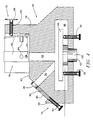
- an AFM 28 according to the present invention in its preferred embodiment are depicted in the cutaway side view of Figure 3.
- a base 30 which, as in the typical prior art AFM, is shock mounted in some manner.
- a piezoelectric scan tube 32 is mounted extending perpendicularly upward from the base 30.
- the scan tube 32 is of a conventional design well known in the art whereby by the application of z-, y-, and z-directional scan voltages to the wires 34, the top end 36 of the tube 32 can be moved horizontally in two orthogonal directions and vertically to provide x and y scanning as well as fine probe positioning in the z direction to the atomic level.
- a sample-holding block 38 is supported on the tips of three adjusting screws 40 threaded through the base 30 employing a hole/slot/surface contact and alignment technique which is well known in the art, to be addressed in greater detail later herein.
- the scan tube 32 extends through a bore 42 in the bottom 44 of the sample-holding block 38 so that the top end 36 thereof is within a chamber 46 within the sample-holding block 38.
- a probe-carrying module 48 is disposed within the chamber 46 and supported on the tips of three adjusting screws 50 threaded through the bottom 44 employing a special application of the above-mentioned hole/slot/surface contact and alignment technique, which will also be addressed in greater detail later herein.
- the probe-carrying module 48 provides the solution to several major problems of prior art AFMs as described above.
- the probe-carrying module 48 is of a transparent material having parallel, planar top and bottom surfaces, 52, 54, respectively.
- the probe-carrying module 48 can be made of quartz, glass, or a plastic such as polycarbonate.
- the substrate 20 having the probe 10 mounted thereto is glued to the bottom surface 54 within an O-ring 56 also glued to the bottom surface 54. As will be described in further detail shortly, this arrangement can be employed to place the probe 10 within a fluid cell which can exist between the bottom surface 54 and the sample 14 within the O-ring 56.
- the steel block 22 of the prior art has been eliminated, as desired.
- the probe tip 16 is automatically aligned with respect to the laser beam 24 in a manner to be described shortly.
- the probe-carrying module 48 can be removed and replaced quickly, accurately, and easily if and when the probe/tip become broken and/or worn.
- the used module 48 can then be returned to the factory for the installation of a new probe 10 under the proper conditions.
- the sample 14 is attached to the top of a removeable sample stage 58.
- a particular sample 14 can be attached easily to the stage 58 at a bench location away from the AFM 28. If desired, a particular sample can be removed temporarily and then be reinserted at a later time.
- the sample stage 58 is magnetically attached to a ferromagnetic electrical interference shield 60 carried by the top end 36 of the scan tube 32.
- the shield 60 prevents electrical interference from the scan voltages applied to the tube 32 and, additionally, the magnetic attachment of the sample stage 58 thereto permits the stage 58 (and attached sample 14) to be slid horizontally in the x and y directions to place the desired area for scanning under the probe tip 16.
- the top of the sample holding block 38 has a flat stage area 62 thereon which is parallel to the bottom 44.
- a bore 64 extends perpendicularly from the stage area 62 into the chamber 46 generally concentrically about a point on the probe-carrying module 48 where the tip 16 of the probe 10 is to be located.
- a laser beam source 66 is carried by a rectangular holding member 68 magnetically attached to the stage area 62 for horizontal sliding movement thereon. The laser beam 24 from the source 66, therefore, shines down the bore 64 to strike the probe 10 from whence it is angularly reflected up bore 70 to strike the detecting surface 72 of a photoelectric sensor 26 (of a type well known in the art which individually forms no part of the novelty of this invention).
- the sensor 26 is adjustably held in a micro detector adjustor 74.
- the source 66 of the laser beam 24 is a holder gripping one end of an optic fiber which has the laser beam 24 from a commercial laser device input thereto at the opposite end to prevent heat buildup from the laser device in the area of the probe 10 and associated apparatus.
- a preferred source 66 would include a laser-emitting diode located within the source 66 itself.
- the horizontal position of the holding member 68 is fine-adjusted in the x and y directions (to place the laser beam 24 exactly on the probe 10 for optimum reflection) by means of a pair of orthogonally oriented micro laser adjustors 76.
- each adjustor 76 comprises a vertical member 78 extending upward from the sample holding block 38 adjacent the stage area 62.
- a leaf spring member 80 extends upward along the inner surface of the vertical member 78 from a point of attachment thereto at 82.
- a magnetic probe 84 extends outward towards the stage area 62 from a point just above the point of attachment 82.
- An adjusting screw 86 is threaded through the vertical member 78 into contact with the leaf spring member 80 near the top of the vertical member 78.
- the adjusting screws 86 have a large diameter turning wheel 88 on the outer end thereof whereby the adjusting screws 86 can be turned easily a fraction of a rotation when horizontally adjusting the position of the holding member 68 on the stage area 62.
- turning the wheel 88 (which can be accomplished easily and smoothly because of the mechanical advantages provided) will result in a very small horizontal movement of the holding member 68, which is desirable in order to be able to accurately accomplish the final positioning of the laser beam 24 on the probe 10.
- the preferred micro detector adjustor 74 comprises a U-shaped slider member 90 magnetically adhering to the sliding surface 92 of the sample holding block 38, which is perpendicular to the bore 70.
- the sensor 26 is held within the sideward-facing U of the slider member 90 by a holder 148 having an area 150 therein sized to the contours of the sensor 26.
- Both the holder 148 and the slider member 90 are held to the sliding surface 92 by magnets 116.
- the slider member 90 is moved up and down by the adjusting screw 94 which is threaded through the slider member 90 between the webs 96 in the sample holding block 38 provided for the purpose.
- the holder 148 is moved sideways by the adjusting screw 152 threaded through the bottom of the U of the slider member 90.
- the position of the adjusting screws 50 (and thereby the position of the probe-carrying module 48 when inserted into the chamber 46) can be set using a calibration blank 98 and height gauge 100 as shown.
- the height gauge 100 is inserted into the bore 42 and the calibration blank 98 is positioned on the adjusting screws 50.
- the screws 50 are then raised and/or lowered, as appropriate, until the calibration blank 98 is just resting evenly on the flat top surface of the height gauge 100. At that point, the screws 50 are set to a height such that when the probe-carrying module 48 is positioned on the screws, the probe tip 16 will be at the desired (and anticipated) probe height as shown.
- the adjusting screws 40 must also be set to a proper height to support the probe-carrying module 48 at a point where the sample surface of a mounted sample to be scanned will be at the probe level anticipated by the calibration procedure just described with respect to Figure 4. This is accomplished using the calibration tool 102 in the manner depicted in Figure 5.
- Calibration tool 102 comprises a yoke 104 having a bottom 106 configured exactly like the bottom 44 of the sample holding block 38, including a bore 42′ for the scan tube 32 to pass through. It should be noted that, as will be seen from a description contained hereinafter, while the adjusting screws 50 of the sample holding block 38 need be adjusted only rarely, the adjusting screws 40 will need to be adjusted whenever the sample 14 is changed.
- the calibration tool 102 also has a short focal length calibration microscope 108 positioned perpendicularly to be above the sample surface 12 when the calibration tool 102 is mounted on the adjusting screws 40.
- the focal length of the calibration microscope 108 is chosen such as to focus exactly at the plane the probe tip 16 will be in.
- the sample 14 is mounted on the scan tube 20 and the calibration tool 102 positioned as shown in Figure 5. While viewing through the calibration microscope 102, the adjusting screws 40 are used to move the calibration tool 102 up and down until the entire surface 12 of the sample 14 is in focus. At that point, the adjusting screws 40 are properly set. Because of the short focal length employed, the surface 12, when completely in focus, is also parallel to the scanning action of the probe 10.
- FIGS 13 and 15 are directly related to the last described aspects of this invention.
- the scanning movement of the piezoelectric scan tube 32 is affected by the application of voltages (which can be in the 100 volt range) to electrodes 110 on the exterior and interior surfaces of the tube 32, which is made of a piezoelectric material.
- voltages which can be in the 100 volt range
- the inventors herein have observed (and proved) that the scanning voltages employed to move the scan tube 32 can still adversely affect the probe 10.
- a disk shaped voltage shield 112 is attached to the top end 36 of the tube 32.
- the shield 112 Since the shield 112 must be electrically conductive, it is attached to the top end 36 of the tube 32 with an insulating adhesive 114. The voltage shield 112 is then physically connected to a ground potential. Optionally, it can be connected to a fixed voltage potential which is available.
- the voltage shield 112 is of a ferro-magnetic material and the sample stage 58 has a magnet 116 mounted therein.
- the voltage shield 112 has a magnet 116 mounted concentrically therein and the sample stage 58 is of a ferro-magnetic material. Accordingly, in either embodiment the voltage shield 112 not only shields against the effects of stray voltages reaching the probe 10; but, additionally, provides a surface on the top end 36 of the scan tube 32 onto which the removeable sample stage 58 having a sample 14 glued thereto can be magnetically attached.
- the sample stage 58 can be slid horizontally in both the x and y directions to place an area of interest under the probe to be scanned thereby.
- the problems of capillary action and friction in soft samples as well as the providing of the gentler and more reliable operation will now be addressed.
- An important aspect of the AFM 28 of this invention is the inclusion of a unique probe design which is, in fact, a microfabricated cantilever with an optical lever as shown in Figures 16 and 17.
- the probe 10 comprises a pair of V-shaped arms 154 formed on the bottom forward edge of the supporting substrate 20 by microfabrication techniques well known in the microelectronics art which, per se, form no part of this invention.
- the arms 154 are, therefore, cantilevered out from the bottom forward edge of the substrate 20. Because of the nature of the materials employed in such microfabrication, the cantilevered arms 154 deflect easily (i.e.
- microfabricated materials have a very smooth surface, they inherently reflect the laser beam 24, thus forming the desired optical lever.
- the actual contacting tip 16 is made of diamond and separately attached where the two arms 154 join to form the "V".
- the problems of capillary action and friction in soft samples can be solved in the AFM 28 of this invention by optionally having the probe 10 and area of the sample being scanned immersed in a fluid bath.
- this novel aspect of the present invention can be accomplished in the manner shown in Figure 6. This approach was employed in early tested embodiments of the present invention; but, has been superceded by the apparatus to be described shortly.
- this embodiment employs the prior art technique of having the probe 10 mounted on a substrate 20 which, in turn, is mounted to a steel block 22, or the like, carried by the base portion of the AFM.
- a clear cover glass 118 is attached to the top of the substrate 20 extending outward over the probe 10.
- a drop of fluid 120 (such as de-ionized water) is then injected with a syringe into the area surrounding the probe 10 defined by the cover glass 118, the sample surface 12, and the edge of the substrate 20, where it adheres by capillary action and surface tension.
- the laser beam 24 passes through the cover glass 118 and fluid 120 to the probe 10 from which it is reflected to pass back through the fluid 120 and cover glass 118. Any minor refraction will remain constant and can be accounted for by adjusting the position of the photoelectric sensor 26.
- the only other problem with this embodiment is that the life of the drop of fluid 120 is limited due to evaporation.
- the probe-carrying module 48 shown in detail in Figures 7 and 8 solves many of the problems associated with the prior art while, when desired or needed, optionally providing the novel fluid cell environment of this invention and is, therefore, the preferred approach.
- Each probe-carrying module 48 is assembled and calibrated (in the manner to be described shortly) at the factory. As mentioned earlier, if the probe 10 wears out or breaks off, the researcher merely installs a new probe-carrying module 48 and sends the broken one back to the factory for recycling.
- the probe-carrying module 48 has an angled area 122 (approximately 10°) cut into the bottom surface 54 into which the probe carrying substrate 20 is glued.
- the probe 10 and substrate 20 are surrounded by an O-ring 56 which is also adhesively attached to the bottom surface 54.
- O-ring 56 When the O-ring 56 is positioned on the surface 12 of the sample 10 as shown in Figure 8, a fluid cell 124 is formed between the bottom surface 54 and the sample surface 12 within the O-ring 56.
- Inlet and outlet tubes 126, 128 are formed into the material of the probe-carrying module 48 communicating with the fluid cell 124 and the exterior of the module 48. Fluid 120 can be injected (or even circulated if applicable) through the tubes 126, 128. The evaporation problem is, therefore, eliminated. It should be noted that where the fluid cell is not needed, the optional probe-carrying module 48 of Figure 18 can be employed.
- the probe-carrying module 48' is of metal or plastic and, as with the above-described version, has an angled area 122 (approximately 10°) cut into the bottom surface 54 into which the probe carrying substrate 20 is glued.
- a bore 156 through the probe-carrying module 48' from the top surface 52 to the bottom surface 54 aligned with the probe 10 is provided to allow the laser beam 24 to pass through the probe-carrying module 48', strike the probe 10, and be reflected therefrom to the photoelectric sensor 26.
- the fluid cell can also be employed for electro-chemical purposes, and the like.
- three additional tubes 158, 160, and 162 are formed into the material of the probe-carrying module 48 communicating with the fluid cell 124 and the exterior of the module 48.
- Each of the tubes contains an electrode 164 extending between the fluid cell 124 on one end and the exterior of the module 48 on the other, at which point electrical connection can be made thereto.
- samples could be "pinned down" to substrates electrically by applying a voltage between one or more of the electrodes 164 in the fluid cell (containing the sample) and the voltage shield 112.
- the presence of the three electrodes 164 i.e. a working electrode, a reference electrode, and an auxiliary electrode
- the prior art hole/slot/support system employed in the invention and mentioned earlier is depicted in simplified form in Figure 9.
- a simpler example is the three legged stool, which will never wobble like its four legged cousin.
- the use of a three point support system is a logical approach.
- the hole/slot/support technique of Figure 9 is commonly employed.
- the surface to be supported has a straight slot 130 formed therein at a first general point of support.
- a hole 132 is formed into the surface in longitudinal alignment with the slot 130 at a second, but specific, point of support.
- the surface to be supported is placed on three supports by first placing one support into the slot 130. The one support is then slid within the slot as required and the article rotated as needed to allow a second of the three supports to be inserted into the hole 132. Two points of support have thus been established. As two points define a line, the two support points only allow rotation of the surface to be supported about the support points in the hole 132 and slot 130. The surface to be supported is then lower (i.e. rotated about the line defined by the first two support points) until the surface to be supported is resting on the third of the three supports. This supporting technique will repeatedly result in the same positioning of the surface to be supported on the three supports,
- the calibration tool 134 of Figures 10 and 11 is employed to position a washer 136 so that the hole in the center of the washer 136 is the hole 132′ which receives the second of the adjusting screws 50.
- the calibration tool 134 has a horizontal base 138 with three pins 140 extending downward therefrom perpendicular to the base 138 and spaced in the same triangular shape as the three adjusting screws 50.
- a microscope 142 is vertically fit into a bore 144 through the base 138 which has the same relationship to the pins 140 that the bore 64 has to the adjusting screws 50.
- Crosshairs 146 within the microscope 142 cross in the approximate position of the laser beam 24 within the bore 64.
- one pin 140 is inserted in the slot 130.
- a washer 136 is placed on the bottom surface 54 and another of the pins 140 is inserted into the hole 132′ thereof and then placed on the bottom surface 54 along with the third pin 140.
- the calibration tool 134 is then slid over the bottom surface 54 to place the probe tip 16 in the center of the crosshairs 146.
- the washer 136 is then glued to the bottom surface 54 by the application of a fast-drying glue. That completes the calibration procedure as the hole 132′ is now fixed so as to place the probe tip 16 in the proper position when the probe-carrying module 48 is used in an AFM 28.
- the micro laser adjustors 76 are then used to precisely place the laser beam 24 on the probe 10 for optimum reflection. Simultaneously, the micro detector adjustor 76 is used to optimally position the photoelectric sensor 26.
- the AFM 28 of this invention can be placed into service for useful work quickly and easily without undue expense of time and without the need for a high degree of technical training. If the procedures as set forth above are followed, the probe 10 is virtually unbreakable as a result of the setup procedure; and, when the probe 10 does wear out or break, it is quickly and easily replaced.
Landscapes
- Physics & Mathematics (AREA)
- Health & Medical Sciences (AREA)
- General Health & Medical Sciences (AREA)
- General Physics & Mathematics (AREA)
- Nuclear Medicine, Radiotherapy & Molecular Imaging (AREA)
- Radiology & Medical Imaging (AREA)
- Chemical & Material Sciences (AREA)
- Nanotechnology (AREA)
- Engineering & Computer Science (AREA)
- Crystallography & Structural Chemistry (AREA)
- Analytical Chemistry (AREA)
- Length Measuring Devices With Unspecified Measuring Means (AREA)
- Microscoopes, Condenser (AREA)
- Optical Measuring Cells (AREA)
- Micro-Organisms Or Cultivation Processes Thereof (AREA)
- Measurement Of Length, Angles, Or The Like Using Electric Or Magnetic Means (AREA)
- Length Measuring Devices By Optical Means (AREA)
- Investigating Or Analysing Biological Materials (AREA)
- Investigating, Analyzing Materials By Fluorescence Or Luminescence (AREA)
- Analysing Materials By The Use Of Radiation (AREA)
- Investigating Or Analysing Materials By Optical Means (AREA)
Claims (19)
- Ein atomisches Kraftmikroskop (28) zum Bestimmen einer Eigenschaft einer Probe (14), umfassend:
eine Sonde (10), die die genannte Probe abtasten kann;
eine Abtasteinrichtung (32) zum Hervorrufen einer relativen Abtastbewegung zwischen der genannten Sonde und der genannten Probe;
eine Fühlereinrichtung (26, 66) zum Erfassen einer Position der genannten Sonde; und gekennzeichnet durch
einen Fluidkörper (120) in Verbindung mit der genannten Probe und in den die genannte Sonde in Berührung mit der genannten Probe so eingetaucht ist, daß während der genannten relativen Abtastbewegung eine kapillare Anziehung zwischen der genannten Sonde und der genannten Probe verringert wird, die durch einen Oberflächenfilm hervorgerufen wird, der auf der genannten Probe wegen der Aussetzung zu der Umgebungsatmosphäre gebildet wird. - Atomisches Kraftmikroskop gemäß Anspruch 1, dadurch gekennzeichnet, daß die genannte Sonde (10) eine Sondenspitze (16) einschließt, die an einem in den Fluidkörper eingetauchten Hebel angeordnet ist.
- Atomisches Kraftmikroskop gemäß Anspruch 1, gekennzeichnet durch:
eine steife Abdeckplatte (52), die auf einer oberen Oberfläche des genannten Fluidkörpers (120) angeordnet ist, um eine Fluidzelle (124) zwischen der genannten Abdeckplatte und der genannten Probe zu begrenzen. - Atomisches Kraftmikroskop gemäß Anspruch 3, dadurch gekennzeichnet, daß:
die genannte steife Abdeckplatte (52) ein optisch transparentes Material umfaßt; und
die genannte Fühlereinrichtung (26, 66) eine optische Einrichtung (26) zum Erfassen einer vertikalen Bewegung der genannten Sonde mittels Licht (24) umfaßt, das auf die genannte Sonde durch die genannte steife Abdeckplatte hindurch angewendet wird. - Atomisches Kraftmikroskop gemäß Anspruch 1, gekennzeichnet durch:
eine Einrichtung zum Austauschen von Fluid (126, 128) innerhalb des genannten Fluidkörpers. - Atomisches Kraftmikroskop gemäß Anspruch 1, 3, 4 oder 5, dadurch gekennzeichnet, daß es umfaßt:
zwei oder mehrere Elektroden (164) in Berührung mit dem genannten Fluidkörper zum Durchführen einer elektrochemischen Reaktion. - Atomisches Kraftmikroskop gemäß Anspruch 1, 3, 4, 5 oder 6, dadurch gekennzeichnet, daß die genannte Abtasteinrichtung umfaßt:
eine Abtastvorrichtung (32); und
ein leitendes Abschirmelement (60) auf einem festen Potential, das zwischen der genannten Sonde und der genannten Abtastvorrichtung zum elektrischen Abschirmen der genannten Sonde gegen die genannte Abtastvorrichtung angeordnet ist. - Atomisches Kraftmikroskop gemäß irgendeinem der vorhergehenden Ansprüche, dadurch gekennzeichnet, daß es umfaßt:
einen entfernbaren Sondenmodul (48), an dem die genannte Sonde fest an einer ausgewählten Stelle angebracht ist. - Atomisches Kraftmikroskop gemäß irgendeinem der vorhergehenden Ansprüche, dadurch gekennzeichnet, daß es umfaßt:
eine verschiebbar bewegbare und entfernbare Probenhalterung (58), die lösbar mit der genannten Abtasteinrichtung gekoppelt ist und an der die genannte Probe angebracht ist. - Atomisches Kraftmikroskop gemäß irgendeinem der vorhergehenden Ansprüche, dadurch gekennzeichnet, daß es umfaßt:
eine Stütze (38), auf der das genannte Ablenkungserfassungssystem und die genannte Sonde angebracht sind; und
eine an der genannten Stütze (74, 76) angebrachte Einrichtung zum Einstellen der Positionierung der genannten Fühlereinrichtung. - Atomisches Kraftmikroskop gemäß Anspruch 8, gekennzeichnet durch:
eine Stütze (134) für den Sondenmodul, die mechanisch mit dem genannten Sondenmodul (48) während des Betriebs des genannten atomischen Kraftmikroskops gekoppelt ist und eine bestimmte, räumliche Anordnung (130, 132, 140) zu der genannten Fühlereinrichtung hat, so daß, wenn der genannte Sondenmodul mechanisch mit der genannten Stütze für den Sondenmodul gekoppelt ist, sich die genannte Sonde in wesentlicher Ausrichtung mit der genannten Fühlereinrichtung befindet. - Das atomische Kraftmikroskop gemäß Anspruch 9, ferner umfassend:
eine magnetische Einrichtung (116), die die genannte Probenhalterung mechanisch, magnetisch mit der genannten Abtasteinrichtung koppelt. - Atomisches Kraftmikroskop gemäß irgendeinem der vorhergehenden Ansprüche, dadurch gekennzeichnet, daß:
die genannte Fühlereinrichtung eine Lichtbündelquelle (66) und eine Lichtbündelerfassungseinrichtung (26) umfaßt; und
die genannte Einstelleinrichtung (74, 76) eine Einrichtung zur Positionierungseinstellung von wenigstens der genannten Lichtbündelquelle oder der genannten Lichtbündelerfassungseinrichtung umfaßt, so daß ein Lichtbündel, das von der genannten Quelle ausgegeben und von der genannten Sonde reflektiert wird, auf die genannte Erfassungseinrichtung auffällt. - Atomisches Kraftmikroskop gemäß Anspruch 7, in dem die genannte Abtastvorrichtung ein piezoelektrisches Rohr (32) umfaßt und die genannte leitende Abschirmung an einem fernliegenden Ende des genannten Rohrs zwischen dem genannten Rohr und der genannten Sonde angebracht ist.
- Verfahren zum Betreiben eines atomischen Kraftmikroskops, in dem eine relative Abtastbewegung zwischen einer Probe (14) und einer Spitze (16) einer an einem Hebel angebrachten Sonde (10) durch eine Abtasteinrichtung (32) erzeugt wird und eine Auslenkung der genannten an einem Hebel angebrachten Sonde durch ein Auslenkungserfassungssystem(26, 66) erfaßt wird, gegkennzeichnet durch die Schritte:
Bereitstellen eines Fluidkörpers (120) in Verbindung mit der Oberfläche (12) der Probe;
Eintauchen der genannten an einem Hebel angebrachten Sonde in den genannten Fluidkörper, um eine kapillare Anziehung zwischen der an einem Hebel befestigten Sonde und der Probe zu verringern, die durch einen Oberflächenfilm bewirkt wird, der auf der genannten Probe wegen der Aussetzung an die Umgebungsatmosphäre gebildet wird; und
Erzeugen der genannten relativen Abtastbewegung zwischen der genannten Sonde und der genannten Probe, während die genannte an einem Hebel angebrachte Probe in den genannten Fluidkörper eingetaucht ist. - Verfahren gemäß Anspruch 15, umfassend:
Anordnen von zwei oder mehreren Elektroden (164) in Berührung mit dem genannten Fluidkörper; und
Anlegen einer Spannung über die genannten Elektroden während des genannten Abtastschrittes, um eine elektrochemische Reaktion in dem genannten Fluid zu erzeugen. - Verfahren gemäß Anspruch 15, bei dem der genannte Schritt des Bereitstellens eines Fluidkörpers umfaßt: Bereitstellen eines Fluidkörpers, der Wasser einschließt.
- Verfahren gemäß Anspruch 15, 16 oder 17, umfassend:
Anordnen einer steifen Abdeckplatte (52) auf einer oberen Oberfläche des genannten Fluidkörpers, um eine Fluidzelle zwischen der genannten Abdeckplatte und der genannten Probe zu begrenzen. - Verfahren gemäß Anspruch 18, umfassend:
der genannte Anordnungsschritt umfaßt Anordnen einer optisch transparenten, steifen Abdeckplatte auf der oberen Oberfläche des genannten Fluidkörpers; und
Erfassen einer vertikalen Bewegung der genannten Sonde mittels Licht, das auf die genannte Sonde durch die genannte optisch transparente, steife Abdeckplatte hindurch angewendet wird.
Priority Applications (2)
| Application Number | Priority Date | Filing Date | Title |
|---|---|---|---|
| EP94118110A EP0650029B1 (de) | 1989-03-13 | 1990-02-16 | Atomkraftmikroskop mit nach Wahl auswechselbarer Flüssigkeitszelle |
| EP98201015A EP0862045B1 (de) | 1989-03-13 | 1990-02-16 | Atomkraftmikroskop mit nach Wahl auswechselbarer Flüssigkeitszelle |
Applications Claiming Priority (2)
| Application Number | Priority Date | Filing Date | Title |
|---|---|---|---|
| US322001 | 1989-03-13 | ||
| US07/322,001 US4935634A (en) | 1989-03-13 | 1989-03-13 | Atomic force microscope with optional replaceable fluid cell |
Related Child Applications (2)
| Application Number | Title | Priority Date | Filing Date |
|---|---|---|---|
| EP94118110A Division EP0650029B1 (de) | 1989-03-13 | 1990-02-16 | Atomkraftmikroskop mit nach Wahl auswechselbarer Flüssigkeitszelle |
| EP94118110.9 Division-Into | 1990-02-16 |
Publications (3)
| Publication Number | Publication Date |
|---|---|
| EP0388023A2 EP0388023A2 (de) | 1990-09-19 |
| EP0388023A3 EP0388023A3 (de) | 1992-01-02 |
| EP0388023B1 true EP0388023B1 (de) | 1995-08-02 |
Family
ID=23252966
Family Applications (3)
| Application Number | Title | Priority Date | Filing Date |
|---|---|---|---|
| EP98201015A Expired - Lifetime EP0862045B1 (de) | 1989-03-13 | 1990-02-16 | Atomkraftmikroskop mit nach Wahl auswechselbarer Flüssigkeitszelle |
| EP90301688A Expired - Lifetime EP0388023B1 (de) | 1989-03-13 | 1990-02-16 | Atomisches Kraftmikroskop mit nach Wahl auswechselbarer Flüssigkeitszelle |
| EP94118110A Expired - Lifetime EP0650029B1 (de) | 1989-03-13 | 1990-02-16 | Atomkraftmikroskop mit nach Wahl auswechselbarer Flüssigkeitszelle |
Family Applications Before (1)
| Application Number | Title | Priority Date | Filing Date |
|---|---|---|---|
| EP98201015A Expired - Lifetime EP0862045B1 (de) | 1989-03-13 | 1990-02-16 | Atomkraftmikroskop mit nach Wahl auswechselbarer Flüssigkeitszelle |
Family Applications After (1)
| Application Number | Title | Priority Date | Filing Date |
|---|---|---|---|
| EP94118110A Expired - Lifetime EP0650029B1 (de) | 1989-03-13 | 1990-02-16 | Atomkraftmikroskop mit nach Wahl auswechselbarer Flüssigkeitszelle |
Country Status (5)
| Country | Link |
|---|---|
| US (2) | US4935634A (de) |
| EP (3) | EP0862045B1 (de) |
| JP (1) | JPH0776696B2 (de) |
| AT (3) | ATE125934T1 (de) |
| DE (3) | DE69021235T2 (de) |
Families Citing this family (154)
| Publication number | Priority date | Publication date | Assignee | Title |
|---|---|---|---|---|
| GB8910566D0 (en) * | 1989-05-08 | 1989-06-21 | Amersham Int Plc | Imaging apparatus and method |
| US5237859A (en) * | 1989-12-08 | 1993-08-24 | Digital Instruments, Inc. | Atomic force microscope |
| US5224376A (en) * | 1989-12-08 | 1993-07-06 | Digital Instruments, Inc. | Atomic force microscope |
| US5103095A (en) * | 1990-05-23 | 1992-04-07 | Digital Instruments, Inc. | Scanning probe microscope employing adjustable tilt and unitary head |
| US5245863A (en) * | 1990-07-11 | 1993-09-21 | Olympus Optical Co., Ltd. | Atomic probe microscope |
| US5394741A (en) * | 1990-07-11 | 1995-03-07 | Olympus Optical Co., Ltd. | Atomic probe microscope |
| US5193383A (en) * | 1990-07-11 | 1993-03-16 | The United States Of America As Represented By The Secretary Of The Navy | Mechanical and surface force nanoprobe |
| JP2501945B2 (ja) * | 1990-08-28 | 1996-05-29 | 三菱電機株式会社 | 原子間力顕微鏡のカンチレバ―及びその製造方法 |
| US5144833A (en) * | 1990-09-27 | 1992-09-08 | International Business Machines Corporation | Atomic force microscopy |
| US5157251A (en) * | 1991-03-13 | 1992-10-20 | Park Scientific Instruments | Scanning force microscope having aligning and adjusting means |
| EP0509856B1 (de) * | 1991-03-15 | 1998-08-12 | Nikon Corporation | Mikroskop bestehend aus Rastertunnelmikroskop kombiniert mit optischem Mikroskop |
| US5155361A (en) * | 1991-07-26 | 1992-10-13 | The Arizona Board Of Regents, A Body Corporate Acting For And On Behalf Of Arizona State University | Potentiostatic preparation of molecular adsorbates for scanning probe microscopy |
| US5317153A (en) * | 1991-08-08 | 1994-05-31 | Nikon Corporation | Scanning probe microscope |
| CH685518A5 (fr) * | 1991-10-15 | 1995-07-31 | Suisse Electronique Microtech | Détecteur interférométrique de résolution atomique, utilisation et procédés de mise en oeuvre. |
| US5254854A (en) * | 1991-11-04 | 1993-10-19 | At&T Bell Laboratories | Scanning microscope comprising force-sensing means and position-sensitive photodetector |
| JP2520049Y2 (ja) * | 1991-12-18 | 1996-12-11 | アルプス電気株式会社 | 光電センサのファイバ保持構造 |
| US5291775A (en) * | 1992-03-04 | 1994-03-08 | Topometrix | Scanning force microscope with integrated optics and cantilever mount |
| US5319960A (en) * | 1992-03-06 | 1994-06-14 | Topometrix | Scanning force microscope |
| US5448399A (en) * | 1992-03-13 | 1995-09-05 | Park Scientific Instruments | Optical system for scanning microscope |
| US5376790A (en) * | 1992-03-13 | 1994-12-27 | Park Scientific Instruments | Scanning probe microscope |
| US5672816A (en) * | 1992-03-13 | 1997-09-30 | Park Scientific Instruments | Large stage system for scanning probe microscopes and other instruments |
| US5218262A (en) * | 1992-04-06 | 1993-06-08 | The Perkin-Elmer Corporation | Apparatus for retaining an electrode by a magnetically shielded magnet |
| US5476006A (en) * | 1992-07-07 | 1995-12-19 | Matsushita Electronics Corporation | Crystal evaluation apparatus and crystal evaluation method |
| US5412980A (en) * | 1992-08-07 | 1995-05-09 | Digital Instruments, Inc. | Tapping atomic force microscope |
| USRE36488E (en) * | 1992-08-07 | 2000-01-11 | Veeco Instruments Inc. | Tapping atomic force microscope with phase or frequency detection |
| US5519212A (en) * | 1992-08-07 | 1996-05-21 | Digital Instruments, Incorporated | Tapping atomic force microscope with phase or frequency detection |
| US5347854A (en) * | 1992-09-22 | 1994-09-20 | International Business Machines Corporation | Two dimensional profiling with a contact force atomic force microscope |
| DE69320753T2 (de) * | 1992-11-06 | 1999-03-25 | Hitachi Construction Machinery Co., Ltd., Tokio/Tokyo | Rasterabtastmikroskop und Verfahren zur Steuerfehlerkorrektur |
| US5260577A (en) * | 1992-11-09 | 1993-11-09 | International Business Machines Corp. | Sample carriage for scanning probe microscope |
| US5400647A (en) * | 1992-11-12 | 1995-03-28 | Digital Instruments, Inc. | Methods of operating atomic force microscopes to measure friction |
| US5463897A (en) * | 1993-08-17 | 1995-11-07 | Digital Instruments, Inc. | Scanning stylus atomic force microscope with cantilever tracking and optical access |
| US5357105A (en) * | 1993-11-09 | 1994-10-18 | Quesant Instrument Corporation | Light modulated detection system for atomic force microscopes |
| US5440920A (en) * | 1994-02-03 | 1995-08-15 | Molecular Imaging Systems | Scanning force microscope with beam tracking lens |
| US5866805A (en) * | 1994-05-19 | 1999-02-02 | Molecular Imaging Corporation Arizona Board Of Regents | Cantilevers for a magnetically driven atomic force microscope |
| US5515719A (en) * | 1994-05-19 | 1996-05-14 | Molecular Imaging Corporation | Controlled force microscope for operation in liquids |
| US5513518A (en) * | 1994-05-19 | 1996-05-07 | Molecular Imaging Corporation | Magnetic modulation of force sensor for AC detection in an atomic force microscope |
| US5753814A (en) * | 1994-05-19 | 1998-05-19 | Molecular Imaging Corporation | Magnetically-oscillated probe microscope for operation in liquids |
| JP3523688B2 (ja) * | 1994-07-06 | 2004-04-26 | オリンパス株式会社 | 試料測定用プローブ装置 |
| JP2936311B2 (ja) * | 1994-09-09 | 1999-08-23 | セイコーインスツルメンツ株式会社 | 液中観察機能付き走査型近視野原子間力顕微鏡 |
| US5466935A (en) * | 1995-01-20 | 1995-11-14 | Quesant Instrument Corporation | Programmable, scanned-probe microscope system and method |
| US5750989A (en) * | 1995-02-10 | 1998-05-12 | Molecular Imaging Corporation | Scanning probe microscope for use in fluids |
| US5621210A (en) * | 1995-02-10 | 1997-04-15 | Molecular Imaging Corporation | Microscope for force and tunneling microscopy in liquids |
| US5675154A (en) * | 1995-02-10 | 1997-10-07 | Molecular Imaging Corporation | Scanning probe microscope |
| US5581082A (en) * | 1995-03-28 | 1996-12-03 | The Regents Of The University Of California | Combined scanning probe and scanning energy microscope |
| US5811802A (en) * | 1995-08-18 | 1998-09-22 | Gamble; Ronald C. | Scanning probe microscope with hollow pivot assembly |
| US5705814A (en) * | 1995-08-30 | 1998-01-06 | Digital Instruments, Inc. | Scanning probe microscope having automatic probe exchange and alignment |
| US5874668A (en) * | 1995-10-24 | 1999-02-23 | Arch Development Corporation | Atomic force microscope for biological specimens |
| US5654546A (en) * | 1995-11-07 | 1997-08-05 | Molecular Imaging Corporation | Variable temperature scanning probe microscope based on a peltier device |
| US5821545A (en) * | 1995-11-07 | 1998-10-13 | Molecular Imaging Corporation | Heated stage for a scanning probe microscope |
| JP2934739B2 (ja) * | 1996-02-20 | 1999-08-16 | セイコーインスツルメンツ株式会社 | 走査型近視野原子間力顕微鏡 |
| US5825020A (en) * | 1996-09-06 | 1998-10-20 | The Regents Of The University Of California | Atomic force microscope for generating a small incident beam spot |
| US5847387A (en) * | 1996-09-10 | 1998-12-08 | Burleigh Instruments, Inc. | Support device and stage assembly for a scanned-probe microscope |
| US5866807A (en) * | 1997-02-04 | 1999-02-02 | Digital Instruments | Method and apparatus for measuring mechanical properties on a small scale |
| US5831153A (en) * | 1997-02-14 | 1998-11-03 | International Business Machines Corporation | Investigation and/or manipulation device for a sample in fluid |
| US6038916A (en) | 1997-07-22 | 2000-03-21 | Digital Instruments | Method and apparatus for measuring energy dissipation by a probe during operation of an atomic force microscope |
| JP3497734B2 (ja) * | 1997-07-24 | 2004-02-16 | オリンパス株式会社 | 走査型プローブ顕微鏡 |
| US5861550A (en) | 1997-10-14 | 1999-01-19 | Raymax Technology, Incorporated | Scanning force microscope |
| US5874669A (en) * | 1997-10-16 | 1999-02-23 | Raymax Technology, Inc. | Scanning force microscope with removable probe illuminator assembly |
| US6138503A (en) * | 1997-10-16 | 2000-10-31 | Raymax Technology, Inc. | Scanning probe microscope system including removable probe sensor assembly |
| US6008489A (en) | 1997-12-03 | 1999-12-28 | Digital Instruments | Method for improving the operation of oscillating mode atomic force microscopes |
| US6093930A (en) | 1998-04-02 | 2000-07-25 | International Business Machnines Corporation | Automatic probe replacement in a scanning probe microscope |
| US5992226A (en) * | 1998-05-08 | 1999-11-30 | The United States Of America As Represented By The Secretary Of The Navy | Apparatus and method for measuring intermolecular interactions by atomic force microscopy |
| WO2000019166A1 (en) * | 1998-09-26 | 2000-04-06 | Xidex Corporation | Multidimensional sensing system for atomic force miscroscopy |
| US6455838B2 (en) | 1998-10-06 | 2002-09-24 | The Regents Of The University Of California | High sensitivity deflection sensing device |
| US5958701A (en) * | 1999-01-27 | 1999-09-28 | The United States Of America As Represented By The Secretary Of The Navy | Method for measuring intramolecular forces by atomic force |
| US6672144B2 (en) * | 1999-03-29 | 2004-01-06 | Veeco Instruments Inc. | Dynamic activation for an atomic force microscope and method of use thereof |
| US6189374B1 (en) * | 1999-03-29 | 2001-02-20 | Nanodevices, Inc. | Active probe for an atomic force microscope and method of use thereof |
| US6185992B1 (en) * | 1999-07-15 | 2001-02-13 | Veeco Instruments Inc. | Method and system for increasing the accuracy of a probe-based instrument measuring a heated sample |
| DE19935570C2 (de) * | 1999-07-30 | 2001-07-05 | Forschungszentrum Juelich Gmbh | Mikromanipulator |
| US6441371B1 (en) | 2000-04-03 | 2002-08-27 | Korea Institute Of Science And Technology | Scanning probe microscope |
| US20020092340A1 (en) * | 2000-10-30 | 2002-07-18 | Veeco Instruments Inc. | Cantilever array sensor system |
| CN1483136A (zh) | 2000-11-30 | 2004-03-17 | 阿赛勒姆研究股份有限公司 | 用于高精度位置测量的改进线性变量差接变压器 |
| RU2210818C2 (ru) * | 2001-04-12 | 2003-08-20 | Зао "Нт-Мдт" | Сканирующий зондовый микроскоп с жидкостной ячейкой |
| RU2210731C2 (ru) * | 2001-04-12 | 2003-08-20 | Зао "Нт-Мдт" | Сканирующий зондовый микроскоп с жидкостной ячейкой |
| JP4076792B2 (ja) * | 2001-06-19 | 2008-04-16 | 独立行政法人科学技術振興機構 | カンチレバーアレイ、その製造方法及びその装置 |
| US20030233870A1 (en) * | 2001-07-18 | 2003-12-25 | Xidex Corporation | Multidimensional sensing system for atomic force microscopy |
| DE10297054T5 (de) * | 2001-07-18 | 2004-10-14 | The Regents Of The University Of California, Oakland | Messkopf für ein Rasterkraftmikroskop und weitere Anwendungen |
| US6779387B2 (en) * | 2001-08-21 | 2004-08-24 | Georgia Tech Research Corporation | Method and apparatus for the ultrasonic actuation of the cantilever of a probe-based instrument |
| US6694817B2 (en) | 2001-08-21 | 2004-02-24 | Georgia Tech Research Corporation | Method and apparatus for the ultrasonic actuation of the cantilever of a probe-based instrument |
| DE10294376D2 (de) * | 2001-09-24 | 2004-08-26 | Jpk Instruments Ag | Vorrichtung und Verfahren für ein Rastersondenmikroskop |
| JP4050055B2 (ja) * | 2002-01-10 | 2008-02-20 | 株式会社リコー | 手書き文字一括変換装置、手書き文字一括変換方法およびプログラム |
| US6912892B2 (en) * | 2002-04-30 | 2005-07-05 | Hewlett-Packard Development Company, L.P. | Atomic force microscope |
| US7143005B2 (en) * | 2002-05-06 | 2006-11-28 | Veeco Instruments Inc. | Image reconstruction method |
| US7155964B2 (en) * | 2002-07-02 | 2007-01-02 | Veeco Instruments Inc. | Method and apparatus for measuring electrical properties in torsional resonance mode |
| US7168301B2 (en) * | 2002-07-02 | 2007-01-30 | Veeco Instruments Inc. | Method and apparatus of driving torsional resonance mode of a probe-based instrument |
| US7076996B2 (en) | 2002-10-31 | 2006-07-18 | Veeco Instruments Inc. | Environmental scanning probe microscope |
| JP4450736B2 (ja) | 2002-12-18 | 2010-04-14 | アサイラム リサーチ コーポレーション | カンチレバー型機器用完全デジタル式コントローラ |
| US7521257B2 (en) * | 2003-02-11 | 2009-04-21 | The Board Of Regents Of The Nevada System Of Higher Education On Behalf Of The University Of Nevada, Reno | Chemical sensor with oscillating cantilevered probe and mechanical stop |
| US7260980B2 (en) * | 2003-03-11 | 2007-08-28 | Adams Jesse D | Liquid cell and passivated probe for atomic force microscopy and chemical sensing |
| EP1644473B1 (de) * | 2003-06-03 | 2014-01-15 | Cantimer Incorporated | Phasenänderungssensor |
| RU2248600C1 (ru) * | 2003-09-26 | 2005-03-20 | Зао "Нт-Мдт" | Сканирующий зондовый микроскоп с электрохимической ячейкой |
| US20060257286A1 (en) * | 2003-10-17 | 2006-11-16 | Adams Jesse D | Self-sensing array of microcantilevers for chemical detection |
| US20050241392A1 (en) * | 2004-03-09 | 2005-11-03 | Lyubchenko Yuri L | Atomic force microscope tip holder for imaging in liquid |
| US7596990B2 (en) * | 2004-04-14 | 2009-10-06 | Veeco Instruments, Inc. | Method and apparatus for obtaining quantitative measurements using a probe based instrument |
| US7107694B2 (en) | 2004-06-29 | 2006-09-19 | Hysitron, Incorporated | Method for observation of microstructural surface features in heterogeneous materials |
| US7253408B2 (en) * | 2004-08-31 | 2007-08-07 | West Paul E | Environmental cell for a scanning probe microscope |
| US7694346B2 (en) | 2004-10-01 | 2010-04-06 | Board Of Regents Of The Nevada System Of Higher Education On Behalf Of The University Of Nevada | Cantilevered probe detector with piezoelectric element |
| US7278298B2 (en) * | 2004-11-30 | 2007-10-09 | The Regents Of The University Of California | Scanner for probe microscopy |
| US7665349B2 (en) * | 2005-04-12 | 2010-02-23 | Veeco Instruments Inc. | Method and apparatus for rapid automatic engagement of a probe |
| US7513142B2 (en) * | 2005-08-12 | 2009-04-07 | Veeco Instruments Inc. | Tracking qualification and self-optimizing probe microscope and method |
| US7421370B2 (en) * | 2005-09-16 | 2008-09-02 | Veeco Instruments Inc. | Method and apparatus for measuring a characteristic of a sample feature |
| US7429732B2 (en) | 2005-09-30 | 2008-09-30 | Veeco Instruments Inc. | Scanning probe microscopy method and apparatus utilizing sample pitch |
| JP4660782B2 (ja) * | 2005-10-31 | 2011-03-30 | セイコーインスツル株式会社 | 液中セル |
| EP2013609A2 (de) * | 2005-12-31 | 2009-01-14 | Carbon Nanoprobes, Inc. | Rasterkraftmikroskop-spitzen-arrays und verfahren zur herstellung davon |
| US7685869B2 (en) * | 2006-03-13 | 2010-03-30 | Asylum Research Corporation | Nanoindenter |
| US7478552B2 (en) * | 2006-03-21 | 2009-01-20 | Veeco Instruments Inc. | Optical detection alignment/tracking method and apparatus |
| US7607342B2 (en) * | 2006-04-26 | 2009-10-27 | Vecco Instruments, Inc. | Method and apparatus for reducing lateral interactive forces during operation of a probe-based instrument |
| US20080006083A1 (en) * | 2006-06-26 | 2008-01-10 | Feinstein Adam J | Apparatus and method of transporting and loading probe devices of a metrology instrument |
| US7748260B2 (en) * | 2006-07-12 | 2010-07-06 | Veeco Instruments Inc. | Thermal mechanical drive actuator, thermal probe and method of thermally driving a probe |
| DE102006043352A1 (de) * | 2006-09-15 | 2008-03-27 | Westfälische Wilhelms-Universität Münster | Einrichtung zum Abtasten einer von einer Flüssigkeit bedeckten Probenoberfläche |
| US7770439B2 (en) * | 2006-10-17 | 2010-08-10 | Veeco Instruments Inc. | Method and apparatus of scanning a sample using a scanning probe microscope |
| US8050802B2 (en) * | 2006-11-03 | 2011-11-01 | Bruker Nano, Inc. | Method and apparatus of compensating for position shift |
| US7617719B2 (en) * | 2006-11-30 | 2009-11-17 | The Dow Chemical Company | Method and apparatus for obtaining material property information of a heterogeneous sample using harmonic resonance imaging |
| KR100825985B1 (ko) * | 2006-12-21 | 2008-04-28 | 파크시스템스 주식회사 | 자동으로 탐침 교환이 가능한 주사 탐침 현미경 |
| US7578176B2 (en) * | 2006-12-22 | 2009-08-25 | Veeco Metrology, Inc. | Systems and methods for utilizing scanning probe shape characterization |
| EP1950764A1 (de) * | 2007-01-23 | 2008-07-30 | Nambition GmbH | Fluidzelle für die Rastersondenmikroskopie oder Kraftsprektroskopie |
| US8166567B2 (en) | 2007-03-16 | 2012-04-24 | Bruker Nano, Inc. | Fast-scanning SPM scanner and method of operating same |
| US8904560B2 (en) | 2007-05-07 | 2014-12-02 | Bruker Nano, Inc. | Closed loop controller and method for fast scanning probe microscopy |
| DE102007034853A1 (de) * | 2007-07-24 | 2009-02-05 | Jpk Instruments Ag | Verfahren und Vorrichtung zur verbesserten mikrofluidischen Versorgung von Proben und Messeinrichtung |
| US7770231B2 (en) | 2007-08-02 | 2010-08-03 | Veeco Instruments, Inc. | Fast-scanning SPM and method of operating same |
| US7823216B2 (en) * | 2007-08-02 | 2010-10-26 | Veeco Instruments Inc. | Probe device for a metrology instrument and method of fabricating the same |
| US7958776B2 (en) * | 2007-09-06 | 2011-06-14 | Chunhai Wang | Atomic force gradient microscope and method of using this microscope |
| WO2009086534A1 (en) * | 2007-12-28 | 2009-07-09 | Veeco Instruments Inc. | Method of fabricating a probe device for a metrology instrument and probe device produced thereby |
| US7759631B2 (en) | 2008-01-22 | 2010-07-20 | Nanosurf Ag | Raster scanning microscope having transparent optical element with inner curved surface |
| KR101873936B1 (ko) | 2008-11-13 | 2018-07-04 | 브루커 나노, 인코퍼레이션. | 탐침형 원자 현미경 |
| US8214917B2 (en) * | 2009-05-29 | 2012-07-03 | Georgia Tech Research Corporation | Molded microfluidic fluid cell for atomic force microscopy |
| US8356714B2 (en) * | 2009-06-02 | 2013-01-22 | Georgia Tech Research Corporation | Microfluidic device for separation of particles |
| US8782811B2 (en) | 2011-04-29 | 2014-07-15 | Bruker Nano, Inc. | Cleaning station for atomic force microscope |
| EP3293527B1 (de) | 2012-06-22 | 2026-01-14 | Bruker Nano, Inc. | Verfahren und vorrichtung zur messung elektrischer eigenschaften unter verwendung eines afm im spitzenkrafterfassungsmodus |
| WO2014138660A1 (en) | 2013-03-08 | 2014-09-12 | Bruker Nano, Inc. | Method and apparatus of physical property measurement using a probe-based nano-localized light source |
| EP4345463A2 (de) | 2013-03-15 | 2024-04-03 | Bruker Nano, Inc. | Chemische nanoidentifizierung einer probe mittels normalisierter nahfeldspektroskopie |
| WO2014144018A2 (en) | 2013-03-15 | 2014-09-18 | Bruker Nano, Inc. | Dual-probe scanning probe microscope |
| US9097737B2 (en) | 2013-11-25 | 2015-08-04 | Oxford Instruments Asylum Research, Inc. | Modular atomic force microscope with environmental controls |
| WO2015127449A1 (en) | 2014-02-24 | 2015-08-27 | Bruker Nano, Inc. | Precise probe placement in automated scanning probe microscopy systems |
| US9739799B2 (en) | 2014-02-28 | 2017-08-22 | Bruker Nano, Inc. | Method and apparatus to compensate for deflection artifacts in an atomic force microscope |
| WO2016085989A1 (en) * | 2014-11-25 | 2016-06-02 | The Trustees Of The University Of Pennsylvania | In situ tribometer and methods of use |
| CN104501752A (zh) * | 2014-12-25 | 2015-04-08 | 中国工程物理研究院机械制造工艺研究所 | 一种圆弧刃金刚石刀具调心装置 |
| CN104793018B (zh) * | 2015-04-08 | 2017-07-14 | 中国科学院长春光学精密机械与物理研究所 | 一种在原子力显微镜下刀具刃口半径检测用刃口定位装置 |
| US10466501B2 (en) * | 2016-05-26 | 2019-11-05 | Ams Sensors Singapore Pte. Ltd. | Optoelectronic modules including an optical system tilted with respect to a focal plane |
| CN106353535A (zh) * | 2016-10-10 | 2017-01-25 | 中国科学院深圳先进技术研究院 | 原位光电多功能耦合原子力显微镜测试系统 |
| US10345337B2 (en) | 2017-04-13 | 2019-07-09 | Bruker Nano, Inc. | Scanning probe microscopy utilizing separable components |
| US10802045B2 (en) | 2018-03-26 | 2020-10-13 | Bruker Nano, Inc. | Large radius probe |
| JP6939686B2 (ja) * | 2018-04-16 | 2021-09-22 | 株式会社島津製作所 | 走査型プローブ顕微鏡及びカンチレバー移動方法 |
| CN108827772A (zh) * | 2018-05-03 | 2018-11-16 | 四川大学 | 一种用于钢丝杨氏测量仪的光杠杆 |
| CN110967524A (zh) * | 2018-09-30 | 2020-04-07 | 天津大学 | 一种原子力显微镜探针夹持器及其换针装置 |
| CN109828124B (zh) * | 2019-03-27 | 2023-09-22 | 西南交通大学 | 一种广配激光头的聚焦高度可调的多探针扫描探测装置 |
| KR102767392B1 (ko) * | 2019-05-03 | 2025-02-14 | 브루커 나노, 아이엔씨. | 토션 윙 프로브 어셈블리 |
| US11796565B2 (en) | 2021-04-09 | 2023-10-24 | Bruker Nano, Inc. | AFM imaging with metrology-preserving real time denoising |
| US11719719B2 (en) | 2021-06-16 | 2023-08-08 | Bruker Nano, Inc. | Metrology probe with built-in angle and method of fabrication thereof |
| US11604210B2 (en) | 2021-07-08 | 2023-03-14 | Bruker Nano, Inc. | AFM imaging with real time drift correction |
| US20260088245A1 (en) * | 2022-10-21 | 2026-03-26 | Cameca Instruments, Inc. | Positioner for analytic instruments within vacuum chamber |
| ES2977089A1 (es) * | 2022-12-29 | 2024-08-19 | Airbus Operations Slu | Dispositivo medidor de tensión eléctrica mediante la interacción de un sistema microelectromecánico y un interferómetro óptico |
| WO2026043682A1 (en) | 2024-02-22 | 2026-02-26 | Bruker Nano, Inc. | Atomic force microscope based infrared spectroscopy with multiple laser pulse repetition rate excitation |
| CN119165018B (zh) * | 2024-08-02 | 2025-10-03 | 福建师范大学 | 测量固-液界面分子力谱的原子力显微镜原位电解池装置 |
Family Cites Families (6)
| Publication number | Priority date | Publication date | Assignee | Title |
|---|---|---|---|---|
| DE3675158D1 (de) * | 1985-11-26 | 1990-11-29 | Ibm | Verfahren und mikroskop zur erzeugung von topographischen bildern unter anwendung atomarer wechselwirkungskraefte mit subaufloesung. |
| JPS62212507A (ja) * | 1986-03-14 | 1987-09-18 | Agency Of Ind Science & Technol | レ−ザ干渉計で校正を不要とした触針式表面形状検出器 |
| DE3610540A1 (de) * | 1986-03-27 | 1987-10-01 | Kernforschungsanlage Juelich | Bewegungseinrichtung zur mikrobewegung von objekten |
| JPH067042B2 (ja) * | 1987-03-25 | 1994-01-26 | 工業技術院長 | 圧電素子微動機構 |
| EP0296262B1 (de) * | 1987-06-22 | 1991-08-28 | International Business Machines Corporation | Verfahren zur Oberflächenuntersuchung mit Nanometer- und Pikosekundenauflösung sowie Laserabgetastetes Rastertunnelmikroskop zur Durchführung des Verfahrens |
| US4823004A (en) * | 1987-11-24 | 1989-04-18 | California Institute Of Technology | Tunnel and field effect carrier ballistics |
-
1989
- 1989-03-13 US US07/322,001 patent/US4935634A/en not_active Ceased
-
1990
- 1990-02-16 EP EP98201015A patent/EP0862045B1/de not_active Expired - Lifetime
- 1990-02-16 AT AT90301688T patent/ATE125934T1/de not_active IP Right Cessation
- 1990-02-16 DE DE69021235T patent/DE69021235T2/de not_active Expired - Lifetime
- 1990-02-16 DE DE69034251T patent/DE69034251D1/de not_active Expired - Lifetime
- 1990-02-16 AT AT98201015T patent/ATE384245T1/de not_active IP Right Cessation
- 1990-02-16 EP EP90301688A patent/EP0388023B1/de not_active Expired - Lifetime
- 1990-02-16 DE DE69032714T patent/DE69032714T2/de not_active Expired - Lifetime
- 1990-02-16 EP EP94118110A patent/EP0650029B1/de not_active Expired - Lifetime
- 1990-02-16 AT AT94118110T patent/ATE172536T1/de not_active IP Right Cessation
- 1990-03-06 JP JP2052871A patent/JPH0776696B2/ja not_active Expired - Lifetime
-
1992
- 1992-06-04 US US07895984 patent/USRE34489F1/en not_active Expired - Lifetime
Also Published As
| Publication number | Publication date |
|---|---|
| EP0388023A3 (de) | 1992-01-02 |
| JPH0776696B2 (ja) | 1995-08-16 |
| DE69034251D1 (de) | 2008-03-06 |
| ATE172536T1 (de) | 1998-11-15 |
| USRE34489F1 (en) | 1999-12-14 |
| EP0862045A3 (de) | 2000-10-04 |
| ATE384245T1 (de) | 2008-02-15 |
| DE69032714D1 (de) | 1998-11-26 |
| EP0650029A3 (de) | 1996-08-28 |
| USRE34489E (en) | 1993-12-28 |
| DE69021235D1 (de) | 1995-09-07 |
| ATE125934T1 (de) | 1995-08-15 |
| EP0650029A2 (de) | 1995-04-26 |
| DE69032714T2 (de) | 1999-06-02 |
| EP0862045A2 (de) | 1998-09-02 |
| JPH02284015A (ja) | 1990-11-21 |
| EP0862045B1 (de) | 2008-01-16 |
| EP0650029B1 (de) | 1998-10-21 |
| EP0388023A2 (de) | 1990-09-19 |
| DE69021235T2 (de) | 1996-01-04 |
| US4935634A (en) | 1990-06-19 |
Similar Documents
| Publication | Publication Date | Title |
|---|---|---|
| EP0650029B1 (de) | Atomkraftmikroskop mit nach Wahl auswechselbarer Flüssigkeitszelle | |
| US6945100B2 (en) | Scanning probe microscope with improved probe tip mount | |
| US5750989A (en) | Scanning probe microscope for use in fluids | |
| US6748794B2 (en) | Method for replacing a probe sensor assembly on a scanning probe microscope | |
| US5714756A (en) | Scanning probe microscope having a single viewing device for on-axis and oblique angle views | |
| US5376790A (en) | Scanning probe microscope | |
| US6057547A (en) | Scanning probe microscope with scan correction | |
| EP0331148B1 (de) | Mikroskop | |
| US5461907A (en) | Imaging, cutting, and collecting instrument and method | |
| US6005251A (en) | Voice coil scanner for use in scanning probe microscope | |
| WO1996024946A9 (en) | Scanning probe microscope for use in fluids | |
| US11789037B2 (en) | Integrated dual-probe rapid in-situ switching measurement method and device of atomic force microscope | |
| JPH0650750A (ja) | 力検知手段を含む走査型顕微鏡 | |
| KR20070100373A (ko) | 주사형 프로브 현미경과 그 측정방법 | |
| KR920005446B1 (ko) | 현미경 장치 | |
| KR100636011B1 (ko) | 결함 검출장치 | |
| JP2008051690A (ja) | 光学式変位検出機構及びそれを用いた表面情報計測装置 | |
| JP2002014023A (ja) | プローブ回転機構、および該プローブ回転機構を有する走査型プローブ顕微鏡 |
Legal Events
| Date | Code | Title | Description |
|---|---|---|---|
| PUAI | Public reference made under article 153(3) epc to a published international application that has entered the european phase |
Free format text: ORIGINAL CODE: 0009012 |
|
| AK | Designated contracting states |
Kind code of ref document: A2 Designated state(s): AT BE CH DE DK ES FR GB GR IT LI LU NL SE |
|
| PUAL | Search report despatched |
Free format text: ORIGINAL CODE: 0009013 |
|
| AK | Designated contracting states |
Kind code of ref document: A3 Designated state(s): AT BE CH DE DK ES FR GB GR IT LI LU NL SE |
|
| 17P | Request for examination filed |
Effective date: 19920609 |
|
| 17Q | First examination report despatched |
Effective date: 19930416 |
|
| GRAA | (expected) grant |
Free format text: ORIGINAL CODE: 0009210 |
|
| AK | Designated contracting states |
Kind code of ref document: B1 Designated state(s): AT BE CH DE DK ES FR GB GR IT LI LU NL SE |
|
| PG25 | Lapsed in a contracting state [announced via postgrant information from national office to epo] |
Ref country code: ES Free format text: THE PATENT HAS BEEN ANNULLED BY A DECISION OF A NATIONAL AUTHORITY Effective date: 19950802 Ref country code: IT Free format text: LAPSE BECAUSE OF FAILURE TO SUBMIT A TRANSLATION OF THE DESCRIPTION OR TO PAY THE FEE WITHIN THE PRESCRIBED TIME-LIMIT;WARNING: LAPSES OF ITALIAN PATENTS WITH EFFECTIVE DATE BEFORE 2007 MAY HAVE OCCURRED AT ANY TIME BEFORE 2007. THE CORRECT EFFECTIVE DATE MAY BE DIFFERENT FROM THE ONE RECORDED. Effective date: 19950802 Ref country code: AT Effective date: 19950802 Ref country code: BE Effective date: 19950802 Ref country code: CH Effective date: 19950802 Ref country code: GR Free format text: LAPSE BECAUSE OF FAILURE TO SUBMIT A TRANSLATION OF THE DESCRIPTION OR TO PAY THE FEE WITHIN THE PRESCRIBED TIME-LIMIT Effective date: 19950802 Ref country code: DK Effective date: 19950802 Ref country code: NL Free format text: LAPSE BECAUSE OF FAILURE TO SUBMIT A TRANSLATION OF THE DESCRIPTION OR TO PAY THE FEE WITHIN THE PRESCRIBED TIME-LIMIT Effective date: 19950802 Ref country code: LI Effective date: 19950802 |
|
| REF | Corresponds to: |
Ref document number: 125934 Country of ref document: AT Date of ref document: 19950815 Kind code of ref document: T |
|
| XX | Miscellaneous (additional remarks) |
Free format text: TEILANMELDUNG 94118110.9 EINGEREICHT AM 16/02/90. |
|
| REF | Corresponds to: |
Ref document number: 69021235 Country of ref document: DE Date of ref document: 19950907 |
|
| ET | Fr: translation filed | ||
| PG25 | Lapsed in a contracting state [announced via postgrant information from national office to epo] |
Ref country code: SE Effective date: 19951102 |
|
| NLV1 | Nl: lapsed or annulled due to failure to fulfill the requirements of art. 29p and 29m of the patents act | ||
| PG25 | Lapsed in a contracting state [announced via postgrant information from national office to epo] |
Ref country code: GB Effective date: 19960216 |
|
| PG25 | Lapsed in a contracting state [announced via postgrant information from national office to epo] |
Ref country code: LU Free format text: LAPSE BECAUSE OF NON-PAYMENT OF DUE FEES Effective date: 19960229 |
|
| PLBE | No opposition filed within time limit |
Free format text: ORIGINAL CODE: 0009261 |
|
| STAA | Information on the status of an ep patent application or granted ep patent |
Free format text: STATUS: NO OPPOSITION FILED WITHIN TIME LIMIT |
|
| 26N | No opposition filed | ||
| GBPC | Gb: european patent ceased through non-payment of renewal fee |
Effective date: 19960216 |
|
| PGFP | Annual fee paid to national office [announced via postgrant information from national office to epo] |
Ref country code: DE Payment date: 20090331 Year of fee payment: 20 |
|
| PGFP | Annual fee paid to national office [announced via postgrant information from national office to epo] |
Ref country code: FR Payment date: 20090217 Year of fee payment: 20 |
|
| PG25 | Lapsed in a contracting state [announced via postgrant information from national office to epo] |
Ref country code: DE Free format text: LAPSE BECAUSE OF EXPIRATION OF PROTECTION Effective date: 20100216 |