EP0388957A2 - Procédé de dépôt de films d'oxyde de tantale et appareillage de dépôt chimique en phase vapeur pour ledit procédé - Google Patents
Procédé de dépôt de films d'oxyde de tantale et appareillage de dépôt chimique en phase vapeur pour ledit procédé Download PDFInfo
- Publication number
- EP0388957A2 EP0388957A2 EP90105440A EP90105440A EP0388957A2 EP 0388957 A2 EP0388957 A2 EP 0388957A2 EP 90105440 A EP90105440 A EP 90105440A EP 90105440 A EP90105440 A EP 90105440A EP 0388957 A2 EP0388957 A2 EP 0388957A2
- Authority
- EP
- European Patent Office
- Prior art keywords
- gas
- vacuum chamber
- tantalum oxide
- tantalum
- oxygen
- Prior art date
- Legal status (The legal status is an assumption and is not a legal conclusion. Google has not performed a legal analysis and makes no representation as to the accuracy of the status listed.)
- Withdrawn
Links
Images
Classifications
-
- C—CHEMISTRY; METALLURGY
- C23—COATING METALLIC MATERIAL; COATING MATERIAL WITH METALLIC MATERIAL; CHEMICAL SURFACE TREATMENT; DIFFUSION TREATMENT OF METALLIC MATERIAL; COATING BY VACUUM EVAPORATION, BY SPUTTERING, BY ION IMPLANTATION OR BY CHEMICAL VAPOUR DEPOSITION, IN GENERAL; INHIBITING CORROSION OF METALLIC MATERIAL OR INCRUSTATION IN GENERAL
- C23C—COATING METALLIC MATERIAL; COATING MATERIAL WITH METALLIC MATERIAL; SURFACE TREATMENT OF METALLIC MATERIAL BY DIFFUSION INTO THE SURFACE, BY CHEMICAL CONVERSION OR SUBSTITUTION; COATING BY VACUUM EVAPORATION, BY SPUTTERING, BY ION IMPLANTATION OR BY CHEMICAL VAPOUR DEPOSITION, IN GENERAL
- C23C16/00—Chemical coating by decomposition of gaseous compounds, without leaving reaction products of surface material in the coating, i.e. chemical vapour deposition [CVD] processes
- C23C16/22—Chemical coating by decomposition of gaseous compounds, without leaving reaction products of surface material in the coating, i.e. chemical vapour deposition [CVD] processes characterised by the deposition of inorganic material, other than metallic material
- C23C16/30—Deposition of compounds, mixtures or solid solutions, e.g. borides, carbides, nitrides
- C23C16/40—Oxides
- C23C16/405—Oxides of refractory metals or yttrium
-
- C—CHEMISTRY; METALLURGY
- C23—COATING METALLIC MATERIAL; COATING MATERIAL WITH METALLIC MATERIAL; CHEMICAL SURFACE TREATMENT; DIFFUSION TREATMENT OF METALLIC MATERIAL; COATING BY VACUUM EVAPORATION, BY SPUTTERING, BY ION IMPLANTATION OR BY CHEMICAL VAPOUR DEPOSITION, IN GENERAL; INHIBITING CORROSION OF METALLIC MATERIAL OR INCRUSTATION IN GENERAL
- C23C—COATING METALLIC MATERIAL; COATING MATERIAL WITH METALLIC MATERIAL; SURFACE TREATMENT OF METALLIC MATERIAL BY DIFFUSION INTO THE SURFACE, BY CHEMICAL CONVERSION OR SUBSTITUTION; COATING BY VACUUM EVAPORATION, BY SPUTTERING, BY ION IMPLANTATION OR BY CHEMICAL VAPOUR DEPOSITION, IN GENERAL
- C23C4/00—Coating by spraying the coating material in the molten state, e.g. by flame, plasma or electric discharge
- C23C4/12—Coating by spraying the coating material in the molten state, e.g. by flame, plasma or electric discharge characterised by the method of spraying
-
- H—ELECTRICITY
- H10—SEMICONDUCTOR DEVICES; ELECTRIC SOLID-STATE DEVICES NOT OTHERWISE PROVIDED FOR
- H10P—GENERIC PROCESSES OR APPARATUS FOR THE MANUFACTURE OR TREATMENT OF DEVICES COVERED BY CLASS H10
- H10P14/00—Formation of materials, e.g. in the shape of layers or pillars
- H10P14/60—Formation of materials, e.g. in the shape of layers or pillars of insulating materials
- H10P14/69—Inorganic materials
- H10P14/692—Inorganic materials composed of oxides, glassy oxides or oxide-based glasses
- H10P14/6938—Inorganic materials composed of oxides, glassy oxides or oxide-based glasses the material containing at least one metal element, e.g. metal oxides, metal oxynitrides or metal oxycarbides
- H10P14/6939—Inorganic materials composed of oxides, glassy oxides or oxide-based glasses the material containing at least one metal element, e.g. metal oxides, metal oxynitrides or metal oxycarbides characterised by the metal
- H10P14/69393—Inorganic materials composed of oxides, glassy oxides or oxide-based glasses the material containing at least one metal element, e.g. metal oxides, metal oxynitrides or metal oxycarbides characterised by the metal the material containing tantalum, e.g. Ta2O5
-
- H—ELECTRICITY
- H10—SEMICONDUCTOR DEVICES; ELECTRIC SOLID-STATE DEVICES NOT OTHERWISE PROVIDED FOR
- H10D—INORGANIC ELECTRIC SEMICONDUCTOR DEVICES
- H10D1/00—Resistors, capacitors or inductors
- H10D1/60—Capacitors
- H10D1/62—Capacitors having potential barriers
- H10D1/66—Conductor-insulator-semiconductor capacitors, e.g. MOS capacitors
-
- H—ELECTRICITY
- H10—SEMICONDUCTOR DEVICES; ELECTRIC SOLID-STATE DEVICES NOT OTHERWISE PROVIDED FOR
- H10D—INORGANIC ELECTRIC SEMICONDUCTOR DEVICES
- H10D1/00—Resistors, capacitors or inductors
- H10D1/60—Capacitors
- H10D1/68—Capacitors having no potential barriers
-
- H—ELECTRICITY
- H10—SEMICONDUCTOR DEVICES; ELECTRIC SOLID-STATE DEVICES NOT OTHERWISE PROVIDED FOR
- H10P—GENERIC PROCESSES OR APPARATUS FOR THE MANUFACTURE OR TREATMENT OF DEVICES COVERED BY CLASS H10
- H10P14/00—Formation of materials, e.g. in the shape of layers or pillars
- H10P14/60—Formation of materials, e.g. in the shape of layers or pillars of insulating materials
- H10P14/63—Formation of materials, e.g. in the shape of layers or pillars of insulating materials characterised by the formation processes
- H10P14/6326—Deposition processes
- H10P14/6328—Deposition from the gas or vapour phase
- H10P14/6334—Deposition from the gas or vapour phase using decomposition or reaction of gaseous or vapour phase compounds, i.e. chemical vapour deposition
- H10P14/6336—Deposition from the gas or vapour phase using decomposition or reaction of gaseous or vapour phase compounds, i.e. chemical vapour deposition in the presence of a plasma [PECVD]
-
- H—ELECTRICITY
- H10—SEMICONDUCTOR DEVICES; ELECTRIC SOLID-STATE DEVICES NOT OTHERWISE PROVIDED FOR
- H10P—GENERIC PROCESSES OR APPARATUS FOR THE MANUFACTURE OR TREATMENT OF DEVICES COVERED BY CLASS H10
- H10P14/00—Formation of materials, e.g. in the shape of layers or pillars
- H10P14/60—Formation of materials, e.g. in the shape of layers or pillars of insulating materials
- H10P14/66—Formation of materials, e.g. in the shape of layers or pillars of insulating materials characterised by the type of materials
- H10P14/662—Laminate layers, e.g. stacks of alternating high-k metal oxides
-
- H—ELECTRICITY
- H10—SEMICONDUCTOR DEVICES; ELECTRIC SOLID-STATE DEVICES NOT OTHERWISE PROVIDED FOR
- H10P—GENERIC PROCESSES OR APPARATUS FOR THE MANUFACTURE OR TREATMENT OF DEVICES COVERED BY CLASS H10
- H10P14/00—Formation of materials, e.g. in the shape of layers or pillars
- H10P14/60—Formation of materials, e.g. in the shape of layers or pillars of insulating materials
- H10P14/69—Inorganic materials
- H10P14/692—Inorganic materials composed of oxides, glassy oxides or oxide-based glasses
- H10P14/6921—Inorganic materials composed of oxides, glassy oxides or oxide-based glasses containing silicon
- H10P14/69215—Inorganic materials composed of oxides, glassy oxides or oxide-based glasses containing silicon the material being a silicon oxide, e.g. SiO2
-
- H—ELECTRICITY
- H10—SEMICONDUCTOR DEVICES; ELECTRIC SOLID-STATE DEVICES NOT OTHERWISE PROVIDED FOR
- H10P—GENERIC PROCESSES OR APPARATUS FOR THE MANUFACTURE OR TREATMENT OF DEVICES COVERED BY CLASS H10
- H10P14/00—Formation of materials, e.g. in the shape of layers or pillars
- H10P14/60—Formation of materials, e.g. in the shape of layers or pillars of insulating materials
- H10P14/69—Inorganic materials
- H10P14/694—Inorganic materials composed of nitrides
- H10P14/6943—Inorganic materials composed of nitrides containing silicon
- H10P14/69433—Inorganic materials composed of nitrides containing silicon the material being a silicon nitride not containing oxygen, e.g. SixNy or SixByNz
Definitions
- This invention relates to a chemical vapor deposition technique and, more particularly, to a chemical vapor deposition technique used in formation of a thin tantalum oxide film for providing an electrical insulation in a semiconductor device by way of example.
- the minimum device dimension of an integrated circuit has been shrunk, and such a continuous scale down requests the dielectric film of, for example, a capacitor to be thinner and thinner.
- the conventional dielectric materials such as silicon oxide and silicon nitride reach the physical limit because direct tunneling current seriously takes place across the dielectric film. Therefore, research and development efforts are being made for a reliable insulating film with an emphasis put on a tantalum oxide films deposited through a chemical vapor deposition technique which is advantageous over a sputtered tantalum oxide film in coverage.
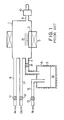
- a prior art chemical vapor deposition system for tantalum oxide films comprises a quartz reactor 1 equipped therein with wafer holder 2, a bubbler 3 coupled through a gas tube 4 to the reactor 1, a heating system 5 for the reactor 1 and the bubbler 3 three gas inlet tubes 6, 7 and 8, a gas outlet tube 9 coupled to a vacuum pump 10, and valves 11, 12, 13 and 14 provided in the gas tubes 6, 7, 8 and 4, respectively.
- the wafer holder 2 retains a plurality of semiconductor wafers 15, and an organotantalum compound 16 such as penta-ethoxy-tantalum (Ta(OC2H5)5) or penta-methoxy-tantalum ((Ta(OCH3)5) is supplied to the bubbler 3.
- an organotantalum compound 16 such as penta-ethoxy-tantalum (Ta(OC2H5)5) or penta-methoxy-tantalum ((Ta(OCH3)5) is supplied to the bubbler 3.
- the vacuum pump 10 is activated and discharges gaseous mixture in the quartz reactor 1.
- the heating system 5 increases the bubbler 3 and the quartz reactor 1 to respective certain temperatures, and a carrier gas of argon is guided through the gas inlet tube 8 to the bubbler 3. Then, the organotantaltum compound is vaporized and flows through the gas tube 4 into the reactor 1, and oxygen gas is further supplied to the quartz reactor 1.
- the organotantalum compound reacts with the oxygen around the semiconductor wafers 15, and tantalum oxide thus produced is deposited on the surfaces of the semiconductor wafers 15.
- the organotantalum compound is heated at 100 degrees to 200 degrees in centigrade, and the temperature in the quartz reactor 1 is fallen within a range from 200 degrees to 600 degrees in centigrade.
- the oxygen gas flow ranges from 0.1 SLM (Standard (state) Litter per Minute) to 5.0 SLM, and the carrier gas flow is regulated between 10 sccm (standard (state) c.c. per minute) to 200 sccm at 0.1 torr to 1.0 torr.
- Such a tantalum oxide is causative of a large amount of leakage current and, accordingly, is not reliable.
- the semiconductor wafer covered with the tantalum oxide film is placed in an electric furnace, and a high temperature heat treatment is carried out in a hydrogen-and-oxygen ambient at about 1000 degrees in centigrade.
- a high temperature heat treatment varies impurity profiles previously formed in the semiconductor wafer, and, for this reason, it is hardly applicable for an ultra large scale integration.
- the present invention proposes to form a tantalum oxide under a plasma-assisted chemical reaction between a tantalum chloride and a nitrogen oxide such as, for example, dinitrogen monoxide.
- the oxygen may be available.
- a process of depositing a tantalum oxide film comprising the steps of a) preparing a reactor with a vacuum chamber associated with a plasma generating unit, b) supplying the vacuum chamber with a tantalum chloride gas and an oxygen-containing gas selected from the group consisting of a dinitrogen monoxide gas represented by the molecular formula of N2O, a nitrogen oxide gas represented by the molecular formula of NO and an oxygen gas represented by the molecular formula of O2, and c) producing a plasma in the vacuum chamber so that plasma-assisted chemical reactions take place for a tantalum oxide.
- a chemical vapor deposition system for producing a tantalum oxide comprising a) a reactor unit having a vacuum chamber, b) a gas source unit coupled to the vacuum chamber for supplying a gaseous mixture containing a tantalum chloride and an oxygen-containing gas selected from the group consisting of a dinitrogen monoxide represented by the molecular formula of N2O, a nitrogen oxide gas represented by the molecular formula of NO and an oxygen gas represented by the molecular formula of O2, and c) a plasma generating unit producing a plasma in the gaseous mixture in the vacuum chamber.
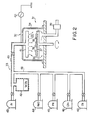
- a chemical vapor deposition system largely comprises a reactor unit 31, a plasma generating unit 32 and a gaseous mixture supplying unit 33.
- the reactor unit 31 has a reactor 34 with a vacuum chamber 35, and a wafer holder 36 accompanied with a heating element 37 projects into the vacuum chamber 35 for retaining semiconductor wafers 38.
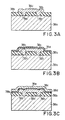
- Each of the semiconductor wafers 38 has an intermediate structure on the way to an integration of semiconductor devices, and is, by way of example, implemented by a silicon substrate 38a partially covered with a silicon dioxide film 38b which in turn is partially covered with a phosphorus-doped polysilicon film 38c for a lower capacitor elec trode connected through contact holes 38f formed in the silicon dioxide film 38b to the substrate 38a as shown in Fig. 3A.
- the vacuum chamber 35 is coupled to a vacuum pump unit 39 so that gaseous mixture is continuously evacuated from the vacuum chamber 35.
- the plasma generating unit 32 has a high frequency electric power source 40 and is operative to produce plasma for promoting chemical reactions in the gaseous mixture.
- the gaseous mixture supplying unit 33 has a gas outlet 41 projecting into the vacuum chamber 35, a vaporizer 42 for tantalum chloride (TaCl5), an argon gas source 43, a dinitrogen monoxide gas source 44, a hydrogen gas source 45, a carbon tetrafluoride gas source 46, an oxygen gas source 47, a pipe network 48 with valve units selectively interconnecting the vaporizer 42, the gas sources 43 to 47 and the reactor 34, and a heating system 49 for the vaporizer 42 as well as the pipe network 48.
- the argon gas conducted into the vaporizer 42 serves as a carrier gas for conveying the tantalum chloride gas into the vacuum chamber 35.
- a chemical vapor deposition process starts with vaporizing the tantalum chloride.
- the heating system 49 supplies heat to the tantalum chloride in the vaporizer 42, and the argon gas is guided from the source 43 into the vaporizer 42.
- the argon gas flow is about 10 sccm to about 200 sccm at 0.1 torr to 10.0 torr.
- the vaporized tantalum chloride is carried on the argon gas, and the gaseous mixture thereof is conducted toward the vacuum chamber 35.
- the dinitrogen monoxide gas is supplied from the source 44 to the pipe network 48, and is mixed into the gaseous mixture on the way to the vacuum chamber 34.
- vaporizer 42 and the pipe between the vaporizer 42 and the reactor 34 are heated at about 50 degrees to about 200 degrees in centigrade, and the dinitrogen monoxide gas is regulated to about 0.1 SLM to about 5.0 SLM.
- the gaseous mixture containing the tantalum chloride, the argon and the dinitrogen monoxide flows into the vacuum chamber by the agency of vacuum created therein.
- the heating element 37 increases the wafer holder 36 and, accordingly, the semiconductor wafers 38 in temperature, and the high frequency electric power source 40 allows plasma to be produced in the gaseous mixture containing the tantalum chloride, the argon and the dinitrogen monoxide thus supplied to the vacuum chamber 35.
- the vacuum chamber 35 is kept in a high temperature ambient ranging between about 100 degrees and about 600 degrees in centigrade.
- the high frequency electric power source 40 produces an alternating current ranging from 50 kHz to 13.56 MHz at 30 watts to 500 watts.
- the process according to the present invention does not need an extremely high temperature ambient, and, for this reason, the heat is less affectable to impurity profiles formed in the semiconductor wafers 38.
- Fig. 3B shows a tantalum oxide film 38d covering the polysilicon film 38c and provides a dielectric film of a capacitor.
- a plate electrode 38e of a turgsten silicide is formed on the tantalum oxide film 38d as shown in Fig. 3C.
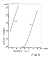
- the tantalum oxide film produced through the process according to the present invention is evaluated in view of dielectric property.
- a tantalum oxide film produced through the prior art process is also evaluated.
- Fig. 4 shows the amount of leakage current in terms of the strength of electric field across dielecric films
- Plots A and B respectively stand for the tantalum oxide film produced through the process according to the present invention (which is related to plots A) and the tantalum oxide film produced through the prior art process using the organotantalum compound. Comparing Plots A with Plots B, it will be understood that the tantalum oxide film produced through the process according to the present invention is advantageous in the dielectric property, and, accordingly, the amount of the leakage current is drastically decreased.
- the reasons why the leakage current is reduced are:
- the tantalum oxide produced through the process according to the present invention has a composition closer to the stoichiometry of Ta2O5.
- the vacuum chamber 35 may be cleaned by using a fluorine containing halogen compound gas for removing residual chlorine from the vacuum chamber 35.
- a halogen compound gas such as carbon tetrafluoride (CF4) is mixed into oxygen and guided to the vacuum chamber 35.
- the carbon tetrafluoride gas ranges from about 0.1 SLM to about 5.0 SLM, and the oxygen gas flow is about 0.1 SLM to about 2.0 SLM.
- the plasma is produced in the gas flow at 50 kHz to 13.56 MHz and about 30 watts to about 500 watts, then residual chlorine is washed away. If the deposition is carried out after the cleaning stage, the reproducibility is improved, and, accordingly, the thickness of the tantalum oxide film 38d is strictly controllable.
- Another process according to the present invention is characterized by hydrogen gas which is further mixed into the gaseous mixture containing the tantalum chloride, the argon and the dinitrogen monoxide.
- the hydrogen gas flow ranges from about 0.1 SLM to about 3.0 SLM, and is conducive to reduction in the amount of undesirable impurities such as chlorine contained in the tantalum oxide film 38d. This is because of the fact that the hydrogen reacts with the chlorine when the tantalum chloride is dissolved into tantalum and chlorine.
- hydrogen gas used in the process according to the present invention further improves the tantalum oxide film in quality.
- Still another process according to the present invention uses oxygen (O2) and nitrogen oxide (NO).
- the process according to the present invention is desirable for producing a tantalum oxide film which is closer to the stoichiometric composition than that produced through the prior art process. Since the tantalum oxide film is high in density but small in the undesirable impurity content as well as in the number of pin holes, the tantalum oxide film produced through the process according to the present invention decreases the amount of leakage current flowing therethrough.
- the tantalum oxide film may be deposited on a substrate of single crystal silicon or of another semiconductor material, a silicide film such as, for example, a tungsten silicide, a polyside film (or a combination of a silicide film and a polysilicon film), a metallic nitride film such as a titanium nitride or a refractory metal film of, for example, tungsten.
- a silicide film such as, for example, a tungsten silicide, a polyside film (or a combination of a silicide film and a polysilicon film)
- a metallic nitride film such as a titanium nitride or a refractory metal film of, for example, tungsten.
- the tantalum oxide film may be combined with a silicon dioxide film or a silicon nitride film to form a multi-level dielectric film structure such as, for example, a tantalum oxide/silicon dioxide film structure or a tantalum oxide/silicon nitride film structure which forms a part of a capacitor.
- the plate electrode 38e may be formed of a refractory metal silicide film except for the tungsten silicide, a polysilicon film, a polyside film, or a metallic nitride film such as a tungsten nitride film.
Landscapes
- Chemical & Material Sciences (AREA)
- Engineering & Computer Science (AREA)
- Mechanical Engineering (AREA)
- Chemical Kinetics & Catalysis (AREA)
- Materials Engineering (AREA)
- Metallurgy (AREA)
- Organic Chemistry (AREA)
- Plasma & Fusion (AREA)
- Physics & Mathematics (AREA)
- Inorganic Chemistry (AREA)
- General Chemical & Material Sciences (AREA)
- Chemical Vapour Deposition (AREA)
- Formation Of Insulating Films (AREA)
- Semiconductor Integrated Circuits (AREA)
Applications Claiming Priority (2)
| Application Number | Priority Date | Filing Date | Title |
|---|---|---|---|
| JP71206/89 | 1989-03-22 | ||
| JP1071206A JPH0641631B2 (ja) | 1989-03-22 | 1989-03-22 | 酸化タンタル膜の化学気相成長法および化学気相成長装置 |
Publications (2)
| Publication Number | Publication Date |
|---|---|
| EP0388957A2 true EP0388957A2 (fr) | 1990-09-26 |
| EP0388957A3 EP0388957A3 (fr) | 1990-10-31 |
Family
ID=13453975
Family Applications (1)
| Application Number | Title | Priority Date | Filing Date |
|---|---|---|---|
| EP19900105440 Withdrawn EP0388957A3 (fr) | 1989-03-22 | 1990-03-22 | Procédé de dépôt de films d'oxyde de tantale et appareillage de dépôt chimique en phase vapeur pour ledit procédé |
Country Status (3)
| Country | Link |
|---|---|
| EP (1) | EP0388957A3 (fr) |
| JP (1) | JPH0641631B2 (fr) |
| KR (1) | KR900014623A (fr) |
Cited By (9)
| Publication number | Priority date | Publication date | Assignee | Title |
|---|---|---|---|---|
| EP0474140A1 (fr) * | 1990-08-31 | 1992-03-11 | Nec Corporation | Procédé pour la formation d'une film isolant capacitif |
| US5580516A (en) * | 1989-06-26 | 1996-12-03 | Cabot Corporation | Powders and products of tantalum, niobium and their alloys |
| WO1998038674A1 (fr) * | 1997-02-27 | 1998-09-03 | Micron Technology, Inc. | Procedes de formation de film a dielectrique eleve, film dielectrique ainsi forme et dispositif correspondant |
| US6566147B2 (en) | 2001-02-02 | 2003-05-20 | Micron Technology, Inc. | Method for controlling deposition of dielectric films |
| US6884475B2 (en) | 2000-05-26 | 2005-04-26 | Micron Technology, Inc. | Chemical vapor deposition method for depositing a high k dielectric film |
| US6888188B2 (en) | 2001-08-17 | 2005-05-03 | Micron Technology, Inc. | Capacitor constructions comprising perovskite-type dielectric materials and having different degrees of crystallinity within the perovskite-type dielectric materials |
| US6943392B2 (en) | 1999-08-30 | 2005-09-13 | Micron Technology, Inc. | Capacitors having a capacitor dielectric layer comprising a metal oxide having multiple different metals bonded with oxygen |
| US6982103B2 (en) | 2001-07-13 | 2006-01-03 | Micron Technology, Inc. | Chemical vapor deposition methods of forming barium strontium titanate comprising dielectric layers, including such layers having a varied concentration of barium and strontium within the layer |
| US7488514B2 (en) | 2001-07-13 | 2009-02-10 | Micron Technology, Inc. | Methods of forming barium strontium titanate layers |
Families Citing this family (3)
| Publication number | Priority date | Publication date | Assignee | Title |
|---|---|---|---|---|
| JP2629579B2 (ja) * | 1993-10-14 | 1997-07-09 | 日本電気株式会社 | 半導体装置の製造方法及び製造装置 |
| KR100447826B1 (ko) * | 2001-11-19 | 2004-09-08 | 주성엔지니어링(주) | 탄탈륨산화막 형성방법 및 그에 사용되는 장치 |
| JP5659079B2 (ja) * | 2011-05-10 | 2015-01-28 | 株式会社アルバック | ZrBO膜の形成装置 |
Family Cites Families (1)
| Publication number | Priority date | Publication date | Assignee | Title |
|---|---|---|---|---|
| DE1812455C3 (de) * | 1968-12-03 | 1980-03-13 | Siemens Ag, 1000 Berlin Und 8000 Muenchen | Verfahren zum Herstellen einer aus einem Metalloxyd bestehenden isolierenden Schutzschicht an der Oberfläche eines Halbleiterkristalls |
-
1989
- 1989-03-22 JP JP1071206A patent/JPH0641631B2/ja not_active Expired - Lifetime
-
1990
- 1990-03-21 KR KR1019900003799A patent/KR900014623A/ko not_active Ceased
- 1990-03-22 EP EP19900105440 patent/EP0388957A3/fr not_active Withdrawn
Cited By (20)
| Publication number | Priority date | Publication date | Assignee | Title |
|---|---|---|---|---|
| US5580516A (en) * | 1989-06-26 | 1996-12-03 | Cabot Corporation | Powders and products of tantalum, niobium and their alloys |
| US5254505A (en) * | 1990-08-31 | 1993-10-19 | Nec Corporation | Process of forming capacitive insulating film |
| EP0474140A1 (fr) * | 1990-08-31 | 1992-03-11 | Nec Corporation | Procédé pour la formation d'une film isolant capacitif |
| US6927179B2 (en) | 1997-02-27 | 2005-08-09 | Micron Technology, Inc. | Methods and apparatus for forming a high dielectric film and the dielectric film formed thereby |
| WO1998038674A1 (fr) * | 1997-02-27 | 1998-09-03 | Micron Technology, Inc. | Procedes de formation de film a dielectrique eleve, film dielectrique ainsi forme et dispositif correspondant |
| US6325017B1 (en) | 1997-02-27 | 2001-12-04 | Micron Technology, Inc. | Apparatus for forming a high dielectric film |
| US7192889B2 (en) | 1997-02-27 | 2007-03-20 | Micron Technology, Inc. | Methods for forming a high dielectric film |
| US6943392B2 (en) | 1999-08-30 | 2005-09-13 | Micron Technology, Inc. | Capacitors having a capacitor dielectric layer comprising a metal oxide having multiple different metals bonded with oxygen |
| US6884475B2 (en) | 2000-05-26 | 2005-04-26 | Micron Technology, Inc. | Chemical vapor deposition method for depositing a high k dielectric film |
| US7052584B2 (en) | 2000-05-26 | 2006-05-30 | Micron Technology, Inc. | Method of forming a capacitor |
| US7217617B2 (en) | 2000-05-26 | 2007-05-15 | Micron Technology, Inc. | Methods of forming a capacitor |
| US6838293B2 (en) | 2001-02-02 | 2005-01-04 | Micron Technology, Inc. | Method for controlling deposition of dielectric films |
| US6962824B2 (en) | 2001-02-02 | 2005-11-08 | Micron Technology, Inc. | Method for controlling deposition of dielectric films |
| US6566147B2 (en) | 2001-02-02 | 2003-05-20 | Micron Technology, Inc. | Method for controlling deposition of dielectric films |
| US6982103B2 (en) | 2001-07-13 | 2006-01-03 | Micron Technology, Inc. | Chemical vapor deposition methods of forming barium strontium titanate comprising dielectric layers, including such layers having a varied concentration of barium and strontium within the layer |
| US7208198B2 (en) | 2001-07-13 | 2007-04-24 | Micron Technology, Inc. | Chemical vapor deposition methods of forming barium strontium titanate comprising dielectric layers, including such layers having a varied concentration of barium and strontium within the layer |
| US7488514B2 (en) | 2001-07-13 | 2009-02-10 | Micron Technology, Inc. | Methods of forming barium strontium titanate layers |
| US6888188B2 (en) | 2001-08-17 | 2005-05-03 | Micron Technology, Inc. | Capacitor constructions comprising perovskite-type dielectric materials and having different degrees of crystallinity within the perovskite-type dielectric materials |
| US6958267B2 (en) | 2001-08-17 | 2005-10-25 | Micron Technology, Inc. | Methods of forming perovskite-type dielectric materials with chemical vapor deposition |
| US7309889B2 (en) | 2001-08-17 | 2007-12-18 | Micron Technology, Inc. | Constructions comprising perovskite-type dielectric |
Also Published As
| Publication number | Publication date |
|---|---|
| JPH0641631B2 (ja) | 1994-06-01 |
| EP0388957A3 (fr) | 1990-10-31 |
| JPH02250970A (ja) | 1990-10-08 |
| KR900014623A (ko) | 1990-10-24 |
Similar Documents
| Publication | Publication Date | Title |
|---|---|---|
| US6544900B2 (en) | In situ dielectric stacks | |
| US5508066A (en) | Method for forming a thin film | |
| KR100355914B1 (ko) | 저온플라즈마를이용한직접회로제조방법 | |
| US6309713B1 (en) | Deposition of tungsten nitride by plasma enhanced chemical vapor deposition | |
| US6569257B1 (en) | Method for cleaning a process chamber | |
| US7172792B2 (en) | Method for forming a high quality low temperature silicon nitride film | |
| US6165916A (en) | Film-forming method and film-forming apparatus | |
| US6649545B2 (en) | Photo-assisted remote plasma apparatus and method | |
| US5326723A (en) | Method for improving stability of tungsten chemical vapor deposition | |
| US6274058B1 (en) | Remote plasma cleaning method for processing chambers | |
| EP0015694B1 (fr) | Procédé de fabrication d'un film isolant sur une surface d'un corps semiconducteur | |
| US5399237A (en) | Etching titanium nitride using carbon-fluoride and carbon-oxide gas | |
| US6208033B1 (en) | Apparatus having titanium silicide and titanium formed by chemical vapor deposition | |
| US6872429B1 (en) | Deposition of tungsten nitride using plasma pretreatment in a chemical vapor deposition chamber | |
| US20030143410A1 (en) | Method for reduction of contaminants in amorphous-silicon film | |
| JPH07118855A (ja) | 複合被膜を沈積する方法 | |
| US6933021B2 (en) | Method of TiSiN deposition using a chemical vapor deposition (CVD) process | |
| US6878625B2 (en) | Method for manufacturing semiconductor device | |
| EP0388957A2 (fr) | Procédé de dépôt de films d'oxyde de tantale et appareillage de dépôt chimique en phase vapeur pour ledit procédé | |
| JPWO2003088342A1 (ja) | 電子デバイス材料の製造方法 | |
| US6335277B2 (en) | Method for forming metal nitride film | |
| JP2611466B2 (ja) | 容量絶縁膜の形成方法 | |
| US6500501B1 (en) | Chemical vapor deposition process for depositing titanium silicide films from an organometallic compound | |
| US7033939B2 (en) | Chemistry for chemical vapor deposition of titanium containing films | |
| JPH11162875A (ja) | 半導体装置の製造方法 |
Legal Events
| Date | Code | Title | Description |
|---|---|---|---|
| PUAI | Public reference made under article 153(3) epc to a published international application that has entered the european phase |
Free format text: ORIGINAL CODE: 0009012 |
|
| PUAL | Search report despatched |
Free format text: ORIGINAL CODE: 0009013 |
|
| 17P | Request for examination filed |
Effective date: 19900322 |
|
| AK | Designated contracting states |
Kind code of ref document: A2 Designated state(s): DE FR GB |
|
| AK | Designated contracting states |
Kind code of ref document: A3 Designated state(s): DE FR GB |
|
| 17Q | First examination report despatched |
Effective date: 19920826 |
|
| STAA | Information on the status of an ep patent application or granted ep patent |
Free format text: STATUS: THE APPLICATION HAS BEEN WITHDRAWN |
|
| 18W | Application withdrawn |
Withdrawal date: 19950105 |