EP0389251B1 - Verfahren zum Betreiben einer Bilddarstellungsvorrichtung - Google Patents
Verfahren zum Betreiben einer Bilddarstellungsvorrichtung Download PDFInfo
- Publication number
- EP0389251B1 EP0389251B1 EP90302998A EP90302998A EP0389251B1 EP 0389251 B1 EP0389251 B1 EP 0389251B1 EP 90302998 A EP90302998 A EP 90302998A EP 90302998 A EP90302998 A EP 90302998A EP 0389251 B1 EP0389251 B1 EP 0389251B1
- Authority
- EP
- European Patent Office
- Prior art keywords
- signal
- pulse
- video signal
- electron beam
- deflection
- Prior art date
- Legal status (The legal status is an assumption and is not a legal conclusion. Google has not performed a legal analysis and makes no representation as to the accuracy of the status listed.)
- Expired - Lifetime
Links
Images







Classifications
-
- G—PHYSICS
- G09—EDUCATION; CRYPTOGRAPHY; DISPLAY; ADVERTISING; SEALS
- G09G—ARRANGEMENTS OR CIRCUITS FOR CONTROL OF INDICATING DEVICES USING STATIC MEANS TO PRESENT VARIABLE INFORMATION
- G09G1/00—Control arrangements or circuits, of interest only in connection with cathode-ray tube indicators; General aspects or details, e.g. selection emphasis on particular characters, dashed line or dotted line generation; Preprocessing of data
-
- G—PHYSICS
- G09—EDUCATION; CRYPTOGRAPHY; DISPLAY; ADVERTISING; SEALS
- G09G—ARRANGEMENTS OR CIRCUITS FOR CONTROL OF INDICATING DEVICES USING STATIC MEANS TO PRESENT VARIABLE INFORMATION
- G09G1/00—Control arrangements or circuits, of interest only in connection with cathode-ray tube indicators; General aspects or details, e.g. selection emphasis on particular characters, dashed line or dotted line generation; Preprocessing of data
- G09G1/20—Control arrangements or circuits, of interest only in connection with cathode-ray tube indicators; General aspects or details, e.g. selection emphasis on particular characters, dashed line or dotted line generation; Preprocessing of data using multi-beam tubes
-
- H—ELECTRICITY
- H01—ELECTRIC ELEMENTS
- H01J—ELECTRIC DISCHARGE TUBES OR DISCHARGE LAMPS
- H01J31/00—Cathode ray tubes; Electron beam tubes
- H01J31/08—Cathode ray tubes; Electron beam tubes having a screen on or from which an image or pattern is formed, picked up, converted, or stored
- H01J31/10—Image or pattern display tubes, i.e. having electrical input and optical output; Flying-spot tubes for scanning purposes
- H01J31/12—Image or pattern display tubes, i.e. having electrical input and optical output; Flying-spot tubes for scanning purposes with luminescent screen
- H01J31/123—Flat display tubes
- H01J31/125—Flat display tubes provided with control means permitting the electron beam to reach selected parts of the screen, e.g. digital selection
- H01J31/126—Flat display tubes provided with control means permitting the electron beam to reach selected parts of the screen, e.g. digital selection using line sources
-
- H—ELECTRICITY
- H04—ELECTRIC COMMUNICATION TECHNIQUE
- H04N—PICTORIAL COMMUNICATION, e.g. TELEVISION
- H04N9/00—Details of colour television systems
- H04N9/12—Picture reproducers
Definitions
- the present invention relates to a method of driving a flat type image display device used as a display for a television receiver or a computer.
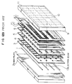
- FIG. 12 is a view showing the construction of a flat type cathode-ray tube which has an internal structure slightly different from that of the display device of the U.S. Patent No. US-A-4 227 117 but displays an image in accordance with the substantially same principle as the display device of the U.S. Patent No. US-A-4 227 117.
- Fig. 12B includes line-like thermionic cathodes 1 (hereinafter referred to as line cathodes) as electron beam emitting sources, a back face electrode 2 which is disposed opposing the line cathodes 1 and on a side reverse to an image display plane, and a plate-like electron beam extracting electrode 3, an electron beam modulating electrode 4, a vertical focusing electrode 5, a horizontal focusing electrode 6, horizontal deflection electrodes 7, 7′, vertical deflection electrodes 8, 8′ and a phosphor-coated screen 9 which are successively disposed opposing the line cathodes 1 and on the same side as the image display plane.
- Fig. 12B is a structural drawing showing a practical structure of conventional flat type cathode-ray tube corresponding to the cathode-ray tube shown in Fig. 12A. These components are accommodated in a flat vacuum glass vessel (not shown).
- Each line cathode 1 as the beam source is stretched in a horizontal direction and a plurality of (L in the explanation and four in the illustration in Fig. 12A or Fig. 12B) such line cathodes are disposed at proper intervals along a vertical direction.
- the line cathode 1 has a structure in which an oxide cathode material is applied on the surface of a tungsten filament of, for example, 20 to 30 »m cross-section.
- the back face electrode 2 made of a conductive plate which may be planar, has a function of suppressing the generation of an electron beam or pushing the generated electron beam toward the display plane side.
- the electron beam extracting electrode 3 is a plate-like electrode having M beam transmissive apertures which are provided at each of, locations opposite to the line cathodes 1-1 to 1-L and at proper intervals in the horizontal direction. A part of an electron beam extracted from the heated line cathode 1 toward the display plane side by the electron beam extracting electrode 3 is passed through the apertures of the electron beam extracting electrode 3. When passed through the apertures, the beam is divided into M beams in the horizontal direction.
- the electron beam modulating electrode 4 provided next to the electron beam extracting electrode 3 is divided into M segments in the horizontal direction so as to permit independent and simultaneous control of the quantities of transmission of the M divisional electron beams from the beam transmissive apertures of the electron beam extracting electrode 3. Only four segments of the electron beam modulating electrode 4 are shown.
- the vertical focusing electrode 5 or the horizontal focusing electrode 6 has slits elongated in the vertical direction or the horizontal direction or apertures elongated in the vertical direction or the horizontal direction and serves to focus each beam in the vertical direction or the horizontal direction.
- the horizontal deflection electrode includes M pairs of electrodes 7 and 7′ with each of the divisional electron beams being sandwiched between the one pair of electrodes 7 and 7′ on opposite sides in the horizontal direction.
- the beam is deflected in the horizontal direction by virtue of a potential difference applied between the paired electrodes 7 and 7′. Since the electrodes 7 in the M pairs and the electrodes 7′ in the M pairs are connected by respective common buses or frames 12, the deflection is made for M beams for each line all at once.
- the vertical deflection electrode includes L pairs of electrodes 8 and 8′ with all of the beams for one line being sandwiched between one pair of electrodes 8 and 8′ on opposite sides in the vertical direction. Each beam is deflected in the vertical direction by virtue of a potential difference applied between the paired electrodes 8 and 8′.
- the electrodes 8 in the L pairs and the electrodes 8′ in the L pairs are connected by respective common buses or frames 12 so as to drive the beams such that the directions of vertical deflection of the beams corresponding to adjacent line cathodes 1 are reversed to each other.
- Electron beams subjected to the focusing, modulation and deflection mentioned above are accelerated by a high voltage applied to the screen 9 so that the electron beams impinge upon phosphors on the screen 9 to excite the phosphors into luminescence.
- the screen 9 is formed by applying three-color (R, G and B) phosphors in stripe shapes with blacks therebetween on a glass plate and depositing a metal back layer on the phosphor stripes.
- the phosphor stripe is formed, for example, so that one pair of R, G and B (or one triplet) correspond to each of the beam transmissive apertures of the electron beam modulating electrode 4.
- Each of image display sections 10 shown by broken lines in Fig. 12 represents a region where an image is displayed by one beam which is passed through the modulating electrode 4 and is deflected in the vertical and horizontal directions.
- the plurality of image display sections 10 are connected on the screen 9 to display one image as a whole.
- Fig. 13 shows a block diagram of the basical driving circuit
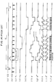
- Fig. 14 shows the waveforms of driving signals for the respective electrodes.
- Reference signals for driving are a vertical synchronizing signal V.D, a horizontal synchronizing signal H.D which are separated from a television video signal 21 at a sync separator circuit 22 and a clock signal generated at a system clock generating circuit 32.
- V.D vertical synchronizing signal
- H.D horizontal synchronizing signal
- the explanation will be made supposing a video signal in an NTSC system. Now, assume that the number of the line cathodes 1 is L.
- L pulses k1 to k L having different phases and each having a low potential during only a period of time corresponding to the width of (240/L)H are generated and are successively applied to the line cathodes 1-1 to 1-L.
- the cathode driving pulses are generated in such a manner that a pulse having a pulse width of (240/L)H is sequentially shifted in a line cathode driving circuit 24 by virtue of trigger pulses p1 to p L each of which is generated by a vertical driving pulse generating circuit 23 each time it counts 240/L horizontal synchronizing signals H.D..
- the back face electrode 2 is applied with a DC potential V2 which is slightly lower than the low potential level of the pulse applied to the line cathode
- the beam extracting electrode 3 is applied with a DC potential V3 which is sufficiently higher than the low potential level of the pulse applied to the line cathode.
- V2 and V3 are supplied from a power source circuit 20.
- the extracted electron beam is modulated in accordance with a video signal voltage including image information.
- a video signal voltage including image information.
- R, G and B phosphors into luminescence for R, G and B video signals, respectively.
- R, G and B video signals are successively applied to the modulating electrodes 4-1 to 4-M on the time-sequential basis in synchronism with the horizontal deflection.
- a video signal 21 is demodulated by a color demodulation circuit 34 into R, G and B signals which in turn are digitized by A/D converters 25-1 to 25-M at each timing triggered by pulses S1 to S M generated at a sampling pulse generating circuit 33 and are then held in video memories 26-1 to 26-M for a period of time 1H.
- the held data are sent to modulating circuits 27-1 to 27-M in a period of time for change-over of 1H in accordance with a read-out pulse f .
- the digital data are converted into analog signals having pulse widths proportional to the values of data or analog signals having pulse amplitudes proportional to the values of data.
- the analog signals are applied to the beam modulating electrodes 4-1 to 4-M in the form of a serial signal of R, G and B by switching pulses S R , S G and S B which are generated at a switching pulse generating circuit 28 synchronizing horizontal driving pulses r, g and b which are generated at a horizontal driving pulse generating circuit 29.
- An example of the modulation signal is shown in Fig. 14, as w .
- the timings of application of the R, G and B pulses are matched to periods of time when the beam is resting on R, G and B phosphors at three steps synchronizing the horizontal driving pulses r, g and b in one horizontal deflection period 1H. Since (M) video signals for one line in the horizontal direction can be simultaneously applied to the modulating electrode 4, there is provided a line-sequencial or line-by-line display system in which an image for one line can be displayed at a time.
- the modulated electron beam is focused in the vertical and horizontal directions by DC potentials V5 and V6, which are generated at the power circuit 20, applied to the vertical focusing electrode 5 and the horizontal focusing electrode 6 and is thereafter electrostatically deflected by the horizontal deflection electrodes 7 and 7′.
- the deflection is effected by stepped deflection waveforms h and h′ shown in Fig. 14 which are generated at a horizontal deflection driving circuit 30.
- the deflection width is selected to be equal to one triplet of R, G and B
- the deflection waveform h or h′ synchnous with the horizontal synchronizing signal H.D takes a stepped waveform in which the voltage is step-wise raised or lowered at every H/3 period synchronizing the horizontal driving pulses r, g and b. Accordingly, the electron beam rests on the R, G and B phosphors for H/3 periods, respectively.
- the horizontal deflection and the vertical deflection are made in the above manner so that one image display section 10 is formed by 3 (in the vertical direction) x 3 (in the horizontal direction) spots excited into luminescence by one electron beam accelerated by a high voltage V9 applied to the screen 9, and such image display sections 10 are regularly arranged on the screen 9 to provide one image.
- the ununiformity of beam landing positions and luminous spot shapes in the vertical direction appears as stepped brightness differences at the boundary portions between adjacent image display sections and the ununiformity of landing positions and luminous spot shapes in the horizontal direction appears as stepped brightness differences or color differences at the boundary portions.
- the ununiformity of beam landing positions is caused from the precision of work and the precision of assemblage of electrodes which contribute to vertical deflection or horizontal deflection in the flat type cathode-ray tube.
- the ununiformity is shape of luminous spots is caused from a change in focusing characteristic of a beam depending on the degree of deflection of the beam which change is produced since the screen plane is planar of flat. This may be prevented by making the deflection angle as small as possible.
- An aim of the present invention is to solve the above problems of the prior art.
- a method of driving a flat type image display device comprising at least a plurality of electron beam generating means, electron beam extracting means, beam quantity controlling means, beam focusing means, beam deflecting means, and luminous means excited into luminescence by impingement of electron beams thereupon, characterised in that the method comprises the step of deflecting an electron beam for making a beam roughly land onto a predetermined position on said luminous means and displacing the beam landing position within a minute range including said predetermined position, and the step of controlling the instant of time of application of a driving signal or the duration of a driving pulse signal for said electron beam quantity controlling means in a form temporally related to the driving of said electron beam deflecting means to control the luminescence of said luminous means.
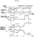
- Fig. 1 shows a phosphor stripe 41 formed on the screen and a beam spot 43 in a form in which the vertical direction and the horizontal direction are interchanged as a matter of convenience.
- the lower portion of Fig. 1 shows a pair of vertical deflection voltage waveforms v and v′ and an electron beam modulating signal waveform w .
- each of the vertical deflection waveforms v and v′ has a waveform in which a sawtooth wave, a triangular wave or another continuously changing voltage waveform having a period of H/3 is superimposed on the conventional stepped voltage waveform (shown by one-dotted chain line in the figure) ascending or descending at every 1H.
- the polarities of change of the deflection voltages v and v′ are made reverse to each other.
- the period of the sawtooth wave is determined by the number of phosphor stripes excited into luminescence through the stepped horizontal deflection of an electron beam during the period of 1H, and the period of H/3 for the sawtooth wave is selected on the assumption that three stripes of R, G and B are excited into luminescence. If the number of horizontal deflection steps is changed, it is necessary to correspondingly change the period of the sawtooth wave.
- the oscillations of respective beam spots take directions of arrow shown in Fig. 3A or Fig. 3B.
- the amplitude of the sawtooth wave is set such that the amplitude of the oscillation falls within about a half of a distance between beam spots 43 and 44 adjacent to each other in the vertical direction on the screen in Fig. 1. The reason is that the deterioration of a resolution due to the overlapping of beam spots 43 and 44 is prevented.
- a beam modulating signal w having a pulse width within the period of H/3 is applied to the electron beam modulating electrode 4.
- a pulse waveform shown by solid line in Fig. 1 is employed as the beam modulating signal w
- the electron beam excites the phosphor 41 into luminescence while moving in the vertical direction in accordance with the vertical deflection voltage waveforms from the instant of time t1 of rise of the pulse w until the instant of time t2 of fall of the pulse w .
- the beam spot 43 moves from a position y1 on the phosphor corresponding to the voltage values v1 and v1′ of the deflection waveforms v and v′ to a position y2 corresponding to the voltage values v2 and v2′.
- the beam spot takes a shape shown by solid line in Fig. 1 and the center position of luminescence thereof is represented by (y1 + y2)/2.
- the beam spot 43 moves from a position y1 + ⁇ y on the phosphor corresponding to the voltage values v1 + ⁇ v and v1′ + ⁇ v of the deflection waveforms v and v′ to a position y2 + ⁇ y corresponding to the voltage values v2 - ⁇ v and v2′ - ⁇ v to provide a spot shape shown by broken line in Fig.
- the center position of luminescence of the beam spot takes a position of (y1 + y2)/2 + ⁇ y or the center position of luminescence is moved by a distance ⁇ y, which provides an effect equivalent to the case where a resting spot is excited into luminescence at the normal landing position.
- the modulating signal pulse is shifted by a time ⁇ t in a direction reverse to that in the above case to move the center of luminescence by - y, thereby bringing it into the normal landing position.
- Stepped vertical deflection voltage waveforms v and v′ used in the conventional method are generated by a known vertical deflection driving block 31 (shown in Fig. 13) in which digital data stored in a memory is D/A converted.
- a sawtooth wave necessary for the present invention is generated by the combination of a counter 50 and a D/A converter 51.
- the counter 50 receives at its CK input terminal, system reference clocks from a system clock generating circuit 32 which have a sufficiently high frequency, and is reset by pulses z synchronous with signals r , g and b which are used for change-over of R, G and B video signals at every H/3 period.
- the output value of the counter 50 is incremented for each clock and is returned to zero simultaneously with resetting of the counter.
- This digital output value of the counter 50 is converted into an analog voltage value by the D/A converter 51, thereby obtaining a sawtooth wave in which a monotonic increase is repeated at a period of H/3.
- a sawtooth wave including a repetitive monotonic decrease can be readily obtained by porality-inverting the output of the D/A converter 52 by an inverting amplifier 52.
- a triangular waveform can be generated by the combination of an up/down counter 54, a D/A converter 55 and a flip-flop 56 shown in Fig. 5.
- the counter 54 is reset by a horizontal synchronizing signal H.D.
- the flip-flop 56 is reset by the horizontal synchronizing signal H.D and takes an output value q which has high and low levels alternated each time the above-mentioned pulse z is inputted.
- the output signal q of the flip-flop 56 is used for changeover of count-up and count-down of the counter 54.
- the output value of the counter 54 monotonically increases in the first H/3 period, monotonically decreases in the next H/3 period and monotonically increases at the further next H/3 period.
- the output value of the counter 55 is converted into an analog value by the D/A converter 55, thereby obtaining a desired waveform.
- a waveform having an inverted polarity is obtained by porality-inverting the output of the D/A converter 55 by an inverting amplifier 57.
- a control memory 60 shown in Fig. 6 for storing digital data for control is prepared for controlling the instant of time of application of a beam modulating signal to a modulating electrode.
- control data corresponding to respective electron beams are successively read from the memory 60 by a trigger signal d having M pulses synchronous with the horizontal synchronizing signal H.D. and are preset into control counters 61-1 to 61-M.
- the counters 61-1 to 61-M start the counting of the system reference clocks from the system clock generating circuit 32 by the signal z synchronous with the horizontal driving pulses r , g and b .
- Each counter generates a carry pulse at a point of time when the preset data value has been counted.
- the carry pulses from the counters 61-1 to 61-M are supplied to video signal memories 26-1 to 26-M so that R, G and B video data are read from the memories.
- the video data read from the memory 26 are supplied to a pulse width modulating circuit 62 for conversion into analog signals having pulse widths corresponding to the data values.
- the analog signals are applied as a serial signal w of R, G and B to the electron beam modualting electrode 4.
- the instant of time of application of the modulating signal is changed by the control data.
- the pulse width modulating circuits 62-1 to 62-M are replaced by D/A converters.
- one control data is allotted to one electron beam. If one control data is allotted to a plurality of electron beams in accordance with the degree of ununiformity in landing of beam spots on the screen 9, the saving of the capacity of the control memory is possible.
- the writing of the control data into the control memory 60 can be made by an external personal computer 64 through an interface circuit 63 separately prepared, thereby making it possible to perform adjustment while visually confirming a change of the position of a beam spot on the screen.
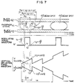
- Fig. 7 shows a phosphor stripe 41 formed on the screen and beam spots 45 and 46 in a form in which the vertical direction and the horizontal direction are interchanged as a matter of convenience.
- the lower portion of Fig. 7 shows a pair of vertical deflection voltage waveforms v and v′ and an electron beam modulating waveform w .
- the vertical deflection waveforms v and v′ may be the same as those explained in conjunction with the embodiment of the first invention and the process of deflection of an electron beam by the vertical deflection waveforms are also the same as that in the first embodiment of the present invention. Therefore, further explanation thereof will be omitted.
- a beam modualting signal w having a pulse width within the period of H/3 is applied to the electron beam modulating electrode 4.
- a pulse waveform shown by solid line in Fig. 7 is employed as the beam modulating signal w , the electron beam excites the phosphor 41 into luminescence while moving in the vertical direction in accordance with the vertical deflection voltage waveforms from the instant of time t1 of the pulse w to the instant of time t2 of fall of the pulse w .
- the beam spot 45 moves from a position y1 on the phosphor corresponding to the voltage values v1 and v1′ of the deflection waveforms v and v′ to a position y2 corresponding to the voltage values v2 and v2′.
- the beam spot has a diameter shown by solid line in Fig. 7 and represented by R s + (y2 - y1) wherein R s is the diameter of a spot excited into luminescence in the case where the beam rests on the phosphor.
- the spot diameter is smaller than a desired spot diameter by ⁇ y.
- the pulse width of the modulating signal is increased by a minute time ⁇ t to provide a pulse width (shown by broken lines) from the instant of time t1 - ⁇ t/2 to the instant of time t2 + ⁇ t/2
- the beam spot 45 moves from a position y1 - ⁇ y/2 corresponding to the voltage values v1 - ⁇ v/2 and v1′ + ⁇ v/2 of the deflection waveforms v and v′ to a position y2 + ⁇ y/2 corresponding to the voltage values v2 + ⁇ v/2 and v2 - ⁇ v/2.
- the beam spot diameter takes a value of R s + (y2 - y1 + ⁇ y) or the spot diameter is increased by ⁇ y as shown by broken lines, thereby obtaining the desired spot diameter.
- the pulse width of the modulating signal is decreased by ⁇ t in contrary to the above case to decrease the spot diameter by ⁇ y, thereby providing the desired value.
- a driving circuit for realizing the control method in the present embodiment will be explained in reference to an example shown in Fig. 8. Since a circuit construction for generating the vertical deflection voltage waveforms v and v′ is the same as that in the embodiment of the first invention, explanation thereof will be omitted.
- a control memory 60 for storing digital data for control.
- control data corresponding to respective electron beams are successively read from the memory 60 by a trigger signal d having M pulses synchronous with the horizontal synchronizing signal H.D, are added to R, G and B video data in adders 65-1 to 65-M, and are stored into video memories 26-1 to 26-M. Accordingly, the widths of pulses converted into analog signals in pulse width modulating circuits 62-1 to 62-M are widened corresponding to the addition of the control data.
- a beam modulating signal the pulse width of which is determined by the control data can be obtained by a circuit construction shown in Fig. 9 or in such a manner that the pulse width modulating circuits 62-1 to 62-M are replaced by D/A converters 66-1 to 66-M, data of the control memory 60 are preset into pulse width control counters 67-1 to 67-M, and RS flip-flops 68-1 to 68-M are set by the trigger signal d having M pulses synchronous with the horizontal synchronizing signal H.D and reset by carry output pulses c of the pulse width control counters 67-1 to 67-M.
- An operation of changing the value of the control data in conformity with the degree of vertical deflection can be performed by an external personal computer 64 through an interface circuit 63 separately prepared, thereby making it possible to perform adjustment while visually confirming a change of the diameter of a beam spot on the screen.
- the pulse width is changed in accordance with the level of a video signal and equally in positive and negative directions around the instant of time when a pulse having the minimum width necessary for representation as an image is to be generated.
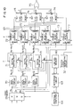
- Fig. 10 shows a circuit diagram of a pulse width modulating circuit in the present embodiment and Fig. 11 shows a time chart of the operation of this circuit.
- M circuits are required out only one circuit is shown for simplification
- R, G and B video digital data after having been stored into a video memory 26 in an 1H period preceding an 1H period when an image is to be displayed, are respectively read from the memory by a trigger signal f synchronous with the horizontal vertical pulses r , g and b and the read data values R v , G v and B v are shifted by one bit toward the lower bit direction in data shift circuits 70 to be reduced to R v /2, G v /2 and B v /2, respectively.
- control data R c , G c and B c are read by the trigger signal f from a control memory 60 in which data determining the center position of a beam modulating pulse is stored, and the shifted video signal data R v /2, G v /2 and B v /2 are subtracted from the control data R c , G c and B c in subtracters 71.
- data R c - R v /2, G c - G v /2 and B c - B v /2 obtained by the operation of subtraction are respectively preset into set counters 72 and at the same time the video data R v , G v and B v are respectively preset into reset counters 73.
- the set counters 72 successively start their counting operations in response to the horizontal deflection pulses r , g and b and generate carry pulses after having counted the preset data.
- the carry pulses are used as set signals for RS flip-flops 74 as well as count start signals for the reset counters 73.
- the reset counters 73 After having made the counting corresponding to the video data R v , G v and B v , the reset counters 73 generate carry pulses to reset the RS flip-flops 74.
- the outputs of the flip-flops 74 produce pulse width-modulated signals w1′, w2′ and w3′ (see Fig. 11) which in turn are converted into a serial signal or a beam modulating signal w by an OR circuit 75.
- the positions of spots on the screen for exciting phosphor into luminescence can be individually controlled for a plurality of electron beams, respectively, it is possible to eliminate brightness differences resulting from localized ununiformity of beam landing positions caused from the precision of work and/or the precision of assemblage of electrodes contributing to the vertical deflection and horizontal deflection in a flat type cathode-ray tube and to eliminate unevenness in brightness even at the boundary portions between image display sections, thereby greatly improving the uniformity of image quality.
- the diameters of spots on the screen for exciting phosphor into luminescence can be individually controlled for a plurality of electron beams, respectively, it is possible to eliminate brightness differences and/or color differences resulting from localized ununiformity of beam spot diameters produced by the vertical deflection and horizontal deflection in a flat type cathode-ray tube and to eliminate unevenness in brightness and/or unevenness in color even at the boundary portions between image display sections, thereby greatly improving the uniformity of image quality.
- the third embodiment even if a beam modulating signal is pulse width-modulated in controlling the position or diameter of a spot on the screen for exciting phosphor into luminescence, this modulation is made without an inconvenience that the position of the beam spot is one-sided to either one of upward and downward directions or either one of rightward and leftward directions on the screen, and there is not a fear that the uniformity of image quality may change between high-light images and low-light images.
Landscapes
- Engineering & Computer Science (AREA)
- Radar, Positioning & Navigation (AREA)
- Remote Sensing (AREA)
- Physics & Mathematics (AREA)
- Computer Hardware Design (AREA)
- General Physics & Mathematics (AREA)
- Theoretical Computer Science (AREA)
- Multimedia (AREA)
- Signal Processing (AREA)
- Transforming Electric Information Into Light Information (AREA)
- Details Of Television Scanning (AREA)
Claims (8)
- Verfahren zum Ansteuern einer Bildanzeigevorrichtung vom flachen Typ, mit mindestens einer Anzahl Elektronenstrahlerzeugungseinrichtungen (1), eine Elektronenstrahlabzieheinrichtung (3), eine Strahlmengensteuereinrichtung (4), eine Strahlfokussiereinrichtung (5, 6), eine Strahlablenkeinrichtung (7, 7′, 8, 8′) und eine Leuchteinrichtung (9), die durch Auftreffen von Elektronenstrahlen darauf zu Lumineszenz angeregt wird, dadurch gekennzeichnet, daß das Verfahren den Schritt des Ablenkens eines Elektronenstrahls, um zu bewirken, daß ein Strahl in etwa auf einer vorbestimmten Position auf der Leuchteinrichtung landet, und des Verschiebens der Strahllandeposition innerhalb eines kleinen Bereiches, einschließlich der vorbestimmten Position, sowie den Schritt des Steuerns des Zeitpunkts des Anlegens eines Ansteuersignals oder der Dauer eines Ansteuerimpulssignals für die Elektronenstrahlmengensteuerungseinrichtung (4) beinhaltet, und zwar in einer Form, die zeitlichen Bezug zu dem Ansteuern der Elektronenstrahlablenkeinrichtung hat, um die Lumineszenz der Leuchteinrichtung zu steuern.
- Verfahren nach Anspruch 1, bei dem der Schritt des Ablenkens des Elektronenstrahls, um zu bewirken, daß der Strahl in etwa auf der vorbestimmten Position auf der Leuchteinrichtung (9) landet, unter Verwendung einer Ablenkeinrichtung (31) ausgeführt wird, die gestufte und periodische Strahlstillstandszeiten hat, und bei dem der Schritt des Verschiebens der Strahllandeposition innerhalb des kleinen Bereiches, einschließlich der vorbestimmten Position, unter Verwendung einer Ablenkeinrichtung (50, 51, 52; 54, 55, 56, 57) ausgeführt wird, die nicht gestuft ist und keine Strahlstillstandszeit hat.
- Verfahren nach Anspruch 2, bei dem die Ablenkeinrichtung zum Bewirken, daß der Elektronenstrahl in etwa auf der vorbestimmten Position auf der Leuchteinrichtung (9) landet, eine elektrostatische Ablenkeinrichtung (31) beinhaltet, die gestufte Spannungswellenformen schafft, und bei dem die Ablenkeinrichtung zum Verschieben der Landeposition innerhalb des kleinen Bereiches, einschließlich der vorbestimmten Position eine elektrostatische Ablenkeinrichtung (50, 51, 52; 54, 55, 56, 57) einschließt, die sägezahnförmige oder dreieckige Spannungswellenformen schafft.
- Verfahren nach Anspruch 1, beinhaltend die Schritte des Erzeugens eines Pulssignaltimings, das abhängig von in einem Steuerspeicher (60) gespeicherten Daten gesteuert wird, des Auslesens eines Videosignals aus einem Videospeicher (26) mittels des Pulssignals, um das Auslese-Videosignal mittels einer Pulsbreitenmodulation oder einer Pulsamplitudenmodulation zu modulieren, und des Anlegens des modulierten Videosignals an eine Strahlmengensteuerelektrode (4).
- Verfahren nach Anspruch 1, beinhaltend die Schritte des Addierens eines Videosignals und in einem Steuerspeicher (60) gesteuerter Daten, um die Pulsbreite des Videosignals mittels der Daten zu steuern, und des Anlegens des pulsbreitenmodulierten Videosignals an eine Strahlmengensteuerelektrode (4).
- Verfahren nach Anspruch 1, beinhaltend die Schritte des Erzeugens eines Pulssignals von pulsbreitengesteuerten Daten, und zwar abhängig von in einem Steuerspeicher (60) gespeicherten Daten, des Auslesens eines Videosignals von einem Videospeicher (26) und Modulierens des Videosignals mittels einer Pulsamplitudenmodulation, die während der gesteuerten Pulsbreite des Pulssignals bewirkt wird, und des Anlegens des modulierten Videosignals an eine Strahlmengensteuerelektrode (4).
- Verfahren nach Anspruch 1, bei dem das Ansteuersignal für die Elektronenstrahlmengensteuereinrichtung (4) ein Signal ist, dessen Pulsbreite mittels eines Videosignals moduliert wird, und bei dem die Pulsbreite des Ansteuersignals entsprechend dem Pegel des Videosignals und jeweils gleich in positiver und negativer Richtung um denjenigen Zeitpunkt herum geändert wird, zu dem ein Signalpuls zu erzeugen ist, der den als ein Videosignal erforderlichen Minimalpegel hat.
- Verfahren nach Anspruch 7, beinhaltend die Schritte des Modulierens des Pulssignals mittels Steuerns des Anstiegstimings des Pulssignals, und zwar durch Steuern derjenigen Daten, die erzeugt werden durch Subtrahieren eines Halb-Amplitudenwertes des Videosignals von in einem Steuerspeicher gesteuerten Daten, und mittels Steuerns des Abfalltimings des Pulssignals durch einen Amplitudenwert des Videosignals und des Anlegens des modulierten Pulssignals an eine Strahlmengensteuerelektrode (4).
Applications Claiming Priority (2)
| Application Number | Priority Date | Filing Date | Title |
|---|---|---|---|
| JP69715/89 | 1989-03-22 | ||
| JP6971589 | 1989-03-22 |
Publications (2)
| Publication Number | Publication Date |
|---|---|
| EP0389251A1 EP0389251A1 (de) | 1990-09-26 |
| EP0389251B1 true EP0389251B1 (de) | 1994-09-28 |
Family
ID=13410806
Family Applications (1)
| Application Number | Title | Priority Date | Filing Date |
|---|---|---|---|
| EP90302998A Expired - Lifetime EP0389251B1 (de) | 1989-03-22 | 1990-03-20 | Verfahren zum Betreiben einer Bilddarstellungsvorrichtung |
Country Status (4)
| Country | Link |
|---|---|
| US (1) | US5061880A (de) |
| EP (1) | EP0389251B1 (de) |
| KR (1) | KR940000897B1 (de) |
| DE (1) | DE69012863T2 (de) |
Families Citing this family (9)
| Publication number | Priority date | Publication date | Assignee | Title |
|---|---|---|---|---|
| JP2823309B2 (ja) * | 1990-03-30 | 1998-11-11 | 三洋電機株式会社 | フラットディスプレイの電極駆動装置 |
| US5525873A (en) * | 1990-05-24 | 1996-06-11 | U.S. Philips Corporation | Picture display device comprising a flat-panel type display unit |
| US5701134A (en) * | 1990-05-24 | 1997-12-23 | U.S. Philips Corporation | Picture display device with uniformity correction of electron supply |
| JP3894523B2 (ja) * | 1998-02-17 | 2007-03-22 | 松下電器産業株式会社 | 容量性負荷の駆動回路 |
| KR100327375B1 (ko) * | 2000-03-06 | 2002-03-06 | 구자홍 | 액티브 구동 장치 |
| US7270543B2 (en) * | 2004-06-29 | 2007-09-18 | Therametric Technologies, Inc. | Handpiece for caries detection |
| US8360771B2 (en) * | 2006-12-28 | 2013-01-29 | Therametric Technologies, Inc. | Handpiece for detection of dental demineralization |
| US20090214089A1 (en) * | 2008-02-27 | 2009-08-27 | Therametric Technologies, Inc. | System and Method for Data Analysis And Capture |
| CN114593680B (zh) * | 2022-02-25 | 2023-12-12 | 南方科技大学 | 一种高精度测量光斑微位移的光学系统及测试方法 |
Family Cites Families (5)
| Publication number | Priority date | Publication date | Assignee | Title |
|---|---|---|---|---|
| FR1457320A (fr) * | 1965-05-28 | 1966-01-24 | Cie Des Produits Elementaires | Dispositif d'affichage d'informations sur un écran de tube cathodique |
| US3440480A (en) * | 1967-01-20 | 1969-04-22 | Bunker Ramo | Display apparatus including means for varying line width |
| US4127796A (en) * | 1977-05-23 | 1978-11-28 | Hughes Aircraft Company | CRT display anti-burn circuit |
| US4227117A (en) * | 1978-04-28 | 1980-10-07 | Matsuhita Electric Industrial Co., Ltd. | Picture display device |
| DE3265125D1 (en) * | 1981-02-10 | 1985-09-12 | Matsushita Electric Industrial Co Ltd | Image display apparatus |
-
1990
- 1990-03-16 US US07/494,627 patent/US5061880A/en not_active Expired - Lifetime
- 1990-03-20 EP EP90302998A patent/EP0389251B1/de not_active Expired - Lifetime
- 1990-03-20 DE DE69012863T patent/DE69012863T2/de not_active Expired - Fee Related
- 1990-03-22 KR KR1019900003917A patent/KR940000897B1/ko not_active Expired - Fee Related
Also Published As
| Publication number | Publication date |
|---|---|
| US5061880A (en) | 1991-10-29 |
| DE69012863T2 (de) | 1995-05-11 |
| DE69012863D1 (de) | 1994-11-03 |
| KR900015051A (ko) | 1990-10-25 |
| EP0389251A1 (de) | 1990-09-26 |
| KR940000897B1 (ko) | 1994-02-04 |
Similar Documents
| Publication | Publication Date | Title |
|---|---|---|
| US4451846A (en) | Color image display apparatus | |
| US4449148A (en) | Image display apparatus | |
| US5061880A (en) | Method of driving image display device | |
| US4523225A (en) | Image display apparatus | |
| EP0398370B1 (de) | Flaches Farb-CRT-Wiedergabegerät mit Abtastkorrektur für den Komponentpositionierungsfehler | |
| US4408143A (en) | Color image display apparatus | |
| JPH0250476B2 (de) | ||
| EP0271926B1 (de) | Bildwiedergabevorrichtung mit einer flachen Kathodenstrahlröhre | |
| US4736139A (en) | Flat type cathode ray tube and color image display apparatus utilizing same | |
| EP0094670B1 (de) | Farbbildwiedergabegerät | |
| US4933604A (en) | Plate-type cathode ray tube device | |
| US4535272A (en) | Image display apparatus | |
| US4988913A (en) | Flat configuration cathode ray tube | |
| EP0079604B1 (de) | Bildwiedergabevorrichtung | |
| JP2538092B2 (ja) | 画像表示素子の駆動方法 | |
| JPH0433195B2 (de) | ||
| JP2652386B2 (ja) | 画像表示装置 | |
| JPH074015B2 (ja) | カラ−画像表示装置 | |
| KR20010029786A (ko) | 소직경의 빔 스포트를 공급할 수 있는 씨알티 시스템 | |
| JP2558462B2 (ja) | 平板形陰極線管の駆動方法 | |
| JP2817149B2 (ja) | 画像表示装置 | |
| JPH074014B2 (ja) | カラ−画像表示装置 | |
| JPS63274991A (ja) | カラ−画像表示装置 | |
| JPH0337793B2 (de) | ||
| JPS62183291A (ja) | カラ−画像表示装置 |
Legal Events
| Date | Code | Title | Description |
|---|---|---|---|
| PUAI | Public reference made under article 153(3) epc to a published international application that has entered the european phase |
Free format text: ORIGINAL CODE: 0009012 |
|
| AK | Designated contracting states |
Kind code of ref document: A1 Designated state(s): DE FR GB |
|
| 17P | Request for examination filed |
Effective date: 19901102 |
|
| 17Q | First examination report despatched |
Effective date: 19930308 |
|
| GRAA | (expected) grant |
Free format text: ORIGINAL CODE: 0009210 |
|
| AK | Designated contracting states |
Kind code of ref document: B1 Designated state(s): DE FR GB |
|
| REF | Corresponds to: |
Ref document number: 69012863 Country of ref document: DE Date of ref document: 19941103 |
|
| ET | Fr: translation filed | ||
| PLBE | No opposition filed within time limit |
Free format text: ORIGINAL CODE: 0009261 |
|
| STAA | Information on the status of an ep patent application or granted ep patent |
Free format text: STATUS: NO OPPOSITION FILED WITHIN TIME LIMIT |
|
| 26N | No opposition filed | ||
| PGFP | Annual fee paid to national office [announced via postgrant information from national office to epo] |
Ref country code: FR Payment date: 19980310 Year of fee payment: 9 |
|
| PGFP | Annual fee paid to national office [announced via postgrant information from national office to epo] |
Ref country code: GB Payment date: 19980311 Year of fee payment: 9 |
|
| PGFP | Annual fee paid to national office [announced via postgrant information from national office to epo] |
Ref country code: DE Payment date: 19980327 Year of fee payment: 9 |
|
| PG25 | Lapsed in a contracting state [announced via postgrant information from national office to epo] |
Ref country code: GB Free format text: LAPSE BECAUSE OF NON-PAYMENT OF DUE FEES Effective date: 19990320 |
|
| GBPC | Gb: european patent ceased through non-payment of renewal fee |
Effective date: 19990320 |
|
| PG25 | Lapsed in a contracting state [announced via postgrant information from national office to epo] |
Ref country code: FR Free format text: LAPSE BECAUSE OF NON-PAYMENT OF DUE FEES Effective date: 19991130 |
|
| REG | Reference to a national code |
Ref country code: FR Ref legal event code: ST |
|
| PG25 | Lapsed in a contracting state [announced via postgrant information from national office to epo] |
Ref country code: DE Free format text: LAPSE BECAUSE OF NON-PAYMENT OF DUE FEES Effective date: 20000101 |