EP0389662B1 - Procédé de réglage de la phase des signaux de deux générateurs d'horloge dans les réseaux de télécommunications - Google Patents
Procédé de réglage de la phase des signaux de deux générateurs d'horloge dans les réseaux de télécommunications Download PDFInfo
- Publication number
- EP0389662B1 EP0389662B1 EP89105713A EP89105713A EP0389662B1 EP 0389662 B1 EP0389662 B1 EP 0389662B1 EP 89105713 A EP89105713 A EP 89105713A EP 89105713 A EP89105713 A EP 89105713A EP 0389662 B1 EP0389662 B1 EP 0389662B1
- Authority
- EP
- European Patent Office
- Prior art keywords
- equipment
- clock signals
- phase
- clock generator
- delay
- Prior art date
- Legal status (The legal status is an assumption and is not a legal conclusion. Google has not performed a legal analysis and makes no representation as to the accuracy of the status listed.)
- Expired - Lifetime
Links
- 238000000034 method Methods 0.000 title claims abstract description 21
- 238000004891 communication Methods 0.000 title description 10
- 230000001360 synchronised effect Effects 0.000 claims abstract description 14
- 238000012937 correction Methods 0.000 claims abstract description 12
- 230000005669 field effect Effects 0.000 claims description 21
- 230000005540 biological transmission Effects 0.000 claims description 13
- 238000012545 processing Methods 0.000 claims description 9
- 238000005516 engineering process Methods 0.000 claims description 7
- 238000012546 transfer Methods 0.000 claims description 3
- 102100027123 55 kDa erythrocyte membrane protein Human genes 0.000 claims description 2
- 101000907578 Homo sapiens Forkhead box protein M1 Proteins 0.000 claims description 2
- 101000590691 Homo sapiens MAGUK p55 subfamily member 2 Proteins 0.000 claims description 2
- 108050007394 Kinesin-like protein KIF20B Proteins 0.000 claims description 2
- 102100032498 MAGUK p55 subfamily member 2 Human genes 0.000 claims description 2
- 239000003990 capacitor Substances 0.000 claims description 2
- 238000003860 storage Methods 0.000 description 24
- JMYNPQVCVQVODQ-OWOJBTEDSA-N 1,3-dichloro-5-[(e)-2-(4-chlorophenyl)ethenyl]benzene Chemical compound C1=CC(Cl)=CC=C1\C=C\C1=CC(Cl)=CC(Cl)=C1 JMYNPQVCVQVODQ-OWOJBTEDSA-N 0.000 description 11
- 101100191136 Arabidopsis thaliana PCMP-A2 gene Proteins 0.000 description 11
- 101150094737 pdm2 gene Proteins 0.000 description 11
- 238000012432 intermediate storage Methods 0.000 description 6
- 101000573165 Dickeya dadantii (strain 3937) Pectinesterase A Proteins 0.000 description 5
- 101000912191 Homo sapiens Cystatin-B Proteins 0.000 description 5
- 238000010586 diagram Methods 0.000 description 5
- 238000005259 measurement Methods 0.000 description 5
- 230000001105 regulatory effect Effects 0.000 description 4
- 230000001934 delay Effects 0.000 description 2
- 238000011161 development Methods 0.000 description 2
- 230000007774 longterm Effects 0.000 description 2
- 239000013643 reference control Substances 0.000 description 2
- 238000006243 chemical reaction Methods 0.000 description 1
- 238000013461 design Methods 0.000 description 1
- 230000000694 effects Effects 0.000 description 1
- 239000010453 quartz Substances 0.000 description 1
- VYPSYNLAJGMNEJ-UHFFFAOYSA-N silicon dioxide Inorganic materials O=[Si]=O VYPSYNLAJGMNEJ-UHFFFAOYSA-N 0.000 description 1
Images

Classifications
-
- H—ELECTRICITY
- H04—ELECTRIC COMMUNICATION TECHNIQUE
- H04J—MULTIPLEX COMMUNICATION
- H04J3/00—Time-division multiplex systems
- H04J3/02—Details
- H04J3/06—Synchronising arrangements
- H04J3/0635—Clock or time synchronisation in a network
- H04J3/0685—Clock or time synchronisation in a node; Intranode synchronisation
- H04J3/0688—Change of the master or reference, e.g. take-over or failure of the master
Definitions
- clock generator devices are provided for the timely switching and transmission of the digital information.
- the clock signals required for timely control of the respective device are generated in these clock generator devices.
- a high-precision, fail-safe clock generator device is installed centrally in synchronously operated communication networks.
- the clock signals generated in this clock generator device are distributed to all components of the communication network together with the digital information, for example voice information, via transmission devices.
- clock generator devices equipped with phase locked loops - phase-locked loops - clock signals are generated in the components, the phases of which coincide with the phases of the incoming high-precision clock signals.
- Such a clock generator device with a phase locked loop is known from the publication 'Proceedings of 1979 ISCAS', pages 804, 805, "A microprocessor-controlled phase-locked loop for network synchronization".
- These clock generator devices ensure timely processing of the digital information in the individual network components. Across from plesiochronous operation of a communication network with synchronous operation the effort per clock generator device with regard to clock accuracy and in particular long-term stability is lower, but this is associated with more complex transmission technology and a spatially limited network structure.
- Fail-safe clock generator devices are provided in the network nodes, in particular digital switching devices, both in plesiochronous operation and in synchronous operation of a communication network.
- Two similarly implemented - d. H. Equipped with phase locked loops - clock generator devices the clock signals of the first clock generator device - hereinafter referred to as reference clock generator device - to the incoming high-precision clock signals and the clock signals of the second clock generator device - hereinafter referred to as clock generator device - are synchronized with the reference clock signals formed by the reference clock generator device. If the reference clock generator device fails, the clock generator device is usually switched over automatically. Since the two clock generator devices, for example in a switching device, are often at some distance - e.g. B.
- phase positions of the clock signals generated in both clock generator devices differ from one another due to the signal propagation times over the connections between the clock generators. If the reference clock generator device fails after switching over to the clock generator device, these phase deviations cause considerable disturbances, in particular in the case of digital information transfer and transmission. This can lead to delays in transmission and possibly to disconnections, particularly in the case of digital data transmission.
- the object on which the invention is based consists in the design of a method with the aid of which it is independent of the distance between two clock generator devices are controlled so that the phases of the clock signals generated in each case in the clock generator devices match.
- the object is solved by the features of claim 1.
- a phase locked loop is also provided in the reference clock generator device, with the aid of which at least one delay device inserted in at least one connecting line is set in such a way that until a phase deviation corresponding to an n times the period of the reference oscillator clock signals is reached.
- This setting variable of the delay line which specifies the phase deviation within the nth oscillator clock signal and the phase deviation in n period lengths of oscillator clock signals, together form correction information which is transmitted to the clock generator device.
- the phases of the clock oscillator signals are corrected in accordance with the phase deviations specified in the correction information.
- An essential advantage of the method according to the invention can be seen in the inclusion of the method for synchronizing clock signals with the aid of a phase locked loop in both clock generator devices.
- proven circuit implementations and, when using a microprocessor, proven program implementations can be included in the implementation according to the invention.
- the method according to the invention is used particularly advantageously in a digital telecommunications exchange.
- clock generator devices can be separated from each other locally, e.g. B. in different frame, can be accommodated. This enables a flexible, modular mechanical structure of digital telecommunications switching systems.
- the correction information is transmitted by pulse duration or pulse pause modulation of the reference clock signals.
- the measured phase deviations between the clock signals of the two clock generator devices are indicated by the pulse duration or pause of the reference clock signals.
- the phase deviation in this is determined by a pulse duration or pulse pause measurement of the reference clock signals transmitted to the clock generator device and the phase of the clock signals is regulated accordingly. Due to this particularly advantageous pulse duration or pulse pause modulation of the reference clock signals, these can be transmitted together with the correction information via a single connection from the reference clock generator to the clock generator device.
- the correction information can alternatively be transmitted in each case by 'm' -coded pulse duration or pulse pause modulated reference clock signals - see claim 3.
- This measure is particularly advantageous if the pulse duration or pulse pause modulation stages are insufficient to represent the required phase deviation values.
- Certain pulse durations or pulse pauses are therefore predetermined logical values - e.g. B. logically "1" or "0" - assigned.
- the chosen code - e.g. B. ten-digit binary code - ten reference clock signals are encoded according to the current phase deviation and transmitted to the clock generator device. These ten reference clock signals are received in the clock generator device and decoded in accordance with the selected coding. The decoded information then represents the phase deviation of the two clock signals measured in the reference clock device.
- the reference oscillator clock signals with respect to their phase or frequency are set in the reference clock device with the aid of an additional reference phase locked loop synchronized with network clock signals brought up to the reference clock generator device - see claim 4.
- This synchronization of the reference clock signals with the network clock signals is provided for reference clock generator devices in synchronously operated communication networks.
- B. Telecommunications exchanges can be distributed.
- phase locked loops When using the already described phase locked loops in the two clock generator devices, a higher control speed is to be provided for the phase locked loop in the clock generator device compared to that in the reference clock generator device - see claim 5 - and a higher control speed for the phase locked loop in the reference clock generator device compared to the reference phase locked loop - see claim 6.
- control speed ratios of the phase-locked loops are particularly advantageous since they prevent instabilities, in particular tendencies to oscillate.
- the frequency of the reference clock and clock signals are matched to a standardized frame or synchronization clock provided for PCM-compatible processing or transmission of information.
- the clock signals derived from the oscillator clock signals each provide the frame clock information, e.g. B. a 32 channel frame clock of a PCM processing clock with 2 Mbit / s. This means that additional effort for adapting the frequency of the clock signals to the frequency of the PCM frame clock or deriving them from the oscillator clock signals is avoided.
- the arrangement for performing the method can be used both as a reference clock generator device and as a clock generator device - see in particular claims 9 and 10.
- information stored in a memory device can be used to set the delay device with a running time of 0 ms and thus to control it ineffectively.
- the delay device is distributed in one of the two or symmetrically in both connecting lines in the reference clock generator and / or the clock generator device inserted - see claim 11.
- the symmetrical division can be achieved by using several smaller, similarly constructed delay devices the same delay time control range as by a single extensive delay device.
- the delay times are determined directly by the control devices or by means of information transmission - for example, again according to claim 2 or 3 to the clock generator device - and set via a storage device provided for this purpose.
- a delay device which can be influenced in terms of the running time is particularly advantageously implemented by means of gates of integrated circuits which can be connected in series - see claim 12.
- the number of gates to be connected in series each of which has a known sound time or delay time, is controlled here by the control device via a storage device.
- a number of gates corresponding to the binary information can be connected in series, for example by forming binary-coded information.
- a flip-flop and three storage devices - see claim 13 - on the one hand the running times of the first delay device can be set by the control device and on the other hand the phase measurement results - lie in n period lengths of oscillator clock signals and in number of parts of a period duration one Oscillator clock signal before - are transmitted to the control device.
- the second delay device can in turn be formed by series-connected gates, the outputs of the gates being connected to the inputs of a control device.
- a positive and a negative comparator device in the second pulse duration modulation device Arranged, whose first comparator inputs are each connected to a memory device and whose second comparator inputs are connected to the outputs of the counting device and the output of the negative comparator device with the set input of a second flip-flop forming the pulse-duration-modulated clock signals and the output of the positive comparator device to a reset input of the second Flip-flop is guided.
- the comparator and memory devices and the second flip-flop the polarity changes of the pulse duration-modulated clock signals to be formed can be varied as required with regard to their occurrence in time. This means that the clock signals can be sent out at any time, ie their phase position can be varied as desired, and the pulse durations of the clock signals, which represent the correction information, can be set as desired.
- a further advantageous embodiment of the invention is to be seen in forming the delay devices by means of a delay chain, the individual delay elements of which are implemented by n- and p-channel field-effect transistors and inverters formed therefrom - see claim 15 20.07.1988 published European patent application 0274606 known.
- the transit time of the signals through the transit time chain is varied by applying a DC voltage or smoothed pulse duration modulated signals to the interconnected gate connections of the transit time chain. If a phase comparator is implemented in addition to the runtime chain in the integrated circuit - see claim 16 -, the generated reference clock signals can be synchronized with the incoming clock signals in the reference clock generator device and the phase deviations can be determined at the same time.
- the level of the smoothed pulse duration modulated signals present at the output of the phase comparison element represents the current phase deviation of the two clock signals.
- the level value must then be digitally processed for further processing in the control device be implemented. This implementation can be accomplished, for example, using commercially available analog-digital conversion devices.
- the additional arrangement of the phase comparison element in the integrated circuit is also known from European patent application 0274606.
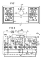
- the clock device TE is formed, for example, in a switching device of a communication network.
- the clock signals tsi required for timely transmission of the information arriving at the switching device are generated in the clock device TE.
- the clock signals tsi thus formed are distributed to all components of the switching system and there, for example, synchronized with the processing clock signals.
- the clock device TE is implemented in the same way from two Clock generator devices RTG, TG built.
- Clock signals tsr, ts are formed in both clock generator devices RTG, TG and are passed to a switching device USE.
- the switching device USE if one clock generator device RTG, TG or the clock signals tsr, ts fails, the other clock generator device RTG, TG or clock signals tsr, ts is switched over.
- the fail-safe clock signals tsi are present at the output A of the switchover device USE and are passed, for example, to the system components of a switching device.
- reference clock generator device RTG In one of the two clock generator devices RTG, TG - hereinafter referred to as reference clock generator device RTG - reference clock signals tsr are formed and transmitted to the other clock generator device TG.
- the clock signals ts formed are synchronized with the incoming reference clock signals tsr with respect to their phase position and transmitted to the reference clock generator device.
- the reference clock generator or clock generator device RTG, TG is formed by a DC voltage controlled oscillator clock device VCO, a counter device MC, a first and second pulse duration modulation device PDM1, PDM2, a phase measuring device PME and a control device RMP, MP.
- FIG. 2 shows a block diagram of a reference clock generator or clock generator device RTG, TG, in which the circuitry components of the first and second pulse duration modulation devices PDM1, PDM2 and the phase measuring device PME are shown in detail.
- a central control device MP the measurement or result information transmitted by the individual devices PDM1, PDM2, PME is evaluated and processed and determined setting information is sent to the corresponding devices PDM1, PDM2, PME.
- the central control device MP is, for example, by an 8-bit microprocessor SAB 8051 from Siemens.
- the setting, measuring and result information is exchanged between the central control device MP and the devices PDM1, PDM2, PME via an intermediate storage device ROM.
- This intermediate storage device ROM is realized by commercially available ROM (Read Only Memory) memory modules.
- the central control device MP accesses the intermediate storage device ROM in the sense of reading and storing information by standardized methods implemented in the control device MP. From this intermediate storage device ROM, the setting information arrives at storage devices RPD, RTF, RNF, RPF, RVZ arranged in the devices PDM1, PDM2, PME, and the measurement and result information is received from storage devices ERG, ERF arranged in the devices PDM1, PDM2, PME this transmitted.
- a voltage-controlled oscillator device VCO consists, for example, of an integrated quartz oscillator circuit and a pull circuit with which the oscillator frequency can be regulated within predetermined limits. Since the pull circuit is usually implemented by capacitance diodes, a frequency change is achieved by varying a DC voltage applied to a voltage input SE of the oscillator device VCO. This DC voltage or drive voltage as is formed in the low-pass device TP with the pulse duration modulated signals pds arriving there.
- the low-pass device TP is implemented, for example, by a low-pass filter connected from a resistor and a capacitor.
- the pulse duration modulated signals pds are generated in a first pulse duration modulation device PDM1.
- the oscillator clock signals ots generated in the oscillator device VCO are fed to a counting input ZE of the counting device MC.
- the transmitted oscillator clock signals ots are continuously binary counted, for example by a 20-bit synchronous counter and the binary-coded count results cs are each provided, for example, at 20 counter outputs arranged in parallel.
- These counting results cs present at the outputs of the counting device MC represent the time base of a clock generator device TG and are fed to the first and second pulse duration modulation devices PDM1, PDM2 and to the phase measuring device PME.
- the count results cs are passed to first 20 inputs of a pulse duration comparator VPD.
- the second 20 inputs of the pulse duration comparator VPD are connected to a pulse duration storage device RPD.
- Pulse duration modulated signals pds are formed in the pulse duration comparator VPD by continuous comparison of the information present at the two 20-bit inputs and are fed to the low-pass device TP via an output of the pulse duration comparator VPD.
- the count results cs are passed to 20 first inputs of a 20-bit AND logic element UD.
- the information stored in a divider memory device RTF is present at 20 second inputs of the 20-bit AND logic element UD.
- This AND logic element UD is used to determine how often the counting results cs are given to the output of the AND logic element UD.
- the frequency and thus the frequency of the transmission of the count results is determined by the information stored in the divider memory device RTF.
- the 20 outputs of the AND gate UD are connected in parallel to 20 inputs of a negative comparator VN and a positive comparator VP.
- the 20 second inputs of the negative comparator VN are connected to the 20 outputs of a negative storage device RNF.
- the 20 second inputs of the positive comparator VP are connected to 20 outputs of a positive memory device RPF.
- the setting information to be stored in the two storage devices RNF, RPF is transmitted by the control device MP via the intermediate storage device ROM transmitted to this.
- a change in polarity towards the positive voltage is indicated in the positive comparator VP and a change in polarity towards the negative voltage is indicated in the negative comparator VN and in each case transmitted to the output of the comparator VN, VP.
- the output of the positive comparator VP is fed to a reset input R and the output of the negative comparator VN to a set input S of a second flip-flop KS2.
- This second flip-flop KS2 is implemented, for example, by an RS flip-flop provided with a set and reset input S, R of an integrated standard circuit technology. With information indicating the polarity change, positive or negative voltage is applied to the output of this second flip-flop KS2.
- the output of this second flip-flop KS2 represents the output of the second pulse duration modulation device PDM2, to which, depending on the use as a reference clock generator or as a clock generator device RTG, TG, either the reference clock signals tsr or the clock signals ts are applied.
- the count results cs are transmitted to 20 inputs of a coarse phase storage device ERG.
- the phase deviations are formed in n periods - n may only take integer values - of the oscillator clock signals ots of the incoming clock signals ts to the internal clock signals tsr, stored and transmitted to the control device MP via the buffer device ROM.
- the times at which the count results cs are to be transferred to the coarse phase storage device ERG are determined by correspondingly applying information - for example a brief positive voltage - to a takeover input of the coarse phase storage device ERG.
- This information determining the time of takeover is formed in a first flip-flop KS1 and is passed via its output and via an OR logic element OD to the takeover input ÜG of the coarse phase storage device ERG.
- the in the oscillator clock signals ots formed by the oscillator device VCO.
- the reference clock signals or clock signals ts, tsr transmitted via a first delay device VZE1 arrive at an input - for example a D input - of the first flip-flop KS1.
- the output of this first flip-flop KS1 is additionally routed to the takeover input ÜF of a second fine phase storage device ERF.
- the first delay device VZE1, VZE2 can be implemented, for example, by connecting gates of integrated circuits of the standard series in series. Smaller groups of series-connected gates can be formed in such a way that the number of gates of the individual groups corresponds to the binary values - for example with groups of one, two, four, eight gates, etc. By inserting a suitable control logic, any number of gates can be connected in series by applying n-digit binary information - for example six digits. In the exemplary embodiment it is assumed that a six-digit binary information is stored in a delay storage device RV and this controls the first delay device VZE1 via six connections in such a way that a number of gates corresponding to the binary information is connected in series - a maximum of 64, for example.
- How many gates are to be connected in series or which information must be stored in the delay storage device RVZ is determined in the control device MP and transmitted to the delay storage device RVZ via the buffer device ROM.
- the output of the first delay device VZE1 is additionally routed to an input of a second delay device VZE2 and at the same time to an input or port MPP1 of the control device MP.
- the clock signals ts, tsr transmitted by the first delay device VZE1 arrive at the input of the second delay device VZE2 implemented as a delay chain.
- the runtime chain is in turn formed by series-connected gates of integrated circuits of the standard series.
- the next change in polarity of the oscillator clock signals ots present at the clock input of the first flip-flop KS1 has the effect that the information present at the inputs of the fine-phase storage device ERF is taken over at exactly this point in time.
- the number of gates of the polarity change of the clock signal ts, tsr passed through indicates the phase deviation within a period of an oscillator clock signal ots. If, for example, the information was transferred to the fine phase storage device ERF at the time when the polarity change of the clock signal ts, tsr has gone through ten gates, the phase deviation of the incoming clock signal ts with the internally formed clock signal ts is ten gate delays.
- the phase deviation is thus 50 ns.
- the number of gates can be increased further, but the outputs of the gates are to be routed via corresponding coding logic, for example binary coding logic. This ensures that, for example, the information from 64 gate outputs can be transmitted in binary code to the fine-phase memory device ERF via six binary-coded lines.
- an output or port MPP2 of the control device MP is connected to the second input of the OR logic element OD .
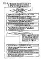
- FIG. 3 in the case of a clock device TE formed according to FIG. 1, the flowchart of the RMP in the reference control device is implemented programs shown or described in detail.
- the clock signals tsr generated in the reference clock generator device RTG do not have to be synchronized with other network clock signals transmitted by a network clock device.
- defined information has to be loaded from the reference control device RMP via the intermediate storage device ROM into the pulse duration storage device RPD.
- FIG. 4 shows the flowchart of the programs implemented in the control device MP of the clock generator device TG and describes them in detail.
- the clock generator device TG is arranged in accordance with FIG. 1 in a clock device TE.
- the individual components of the first and second pulse duration modulation devices PDM1, PDM2, the counting device MC and the phase measuring device PME are - with the exception of the control device - due to the increased processing speeds that occur due to customary integrated circuits - for example the memory devices using commercially available register circuits and other components as already explained - or to realize particularly advantageously by the integrated circuits in ASIC (Application Specified Integrated Circuit) technology. Since in the meantime integrated circuits in ASIC technology are available, which also include microprocessor systems, a reference clock generator or clock generator device RTG, TG can be completely accommodated in an ASIC circuit.
- ASIC Application Specified Integrated Circuit
Landscapes
- Engineering & Computer Science (AREA)
- Computer Networks & Wireless Communication (AREA)
- Signal Processing (AREA)
- Stabilization Of Oscillater, Synchronisation, Frequency Synthesizers (AREA)
- Synchronisation In Digital Transmission Systems (AREA)
Claims (16)
- Procédé pour synchroniser la phase ou la fréquence de signaux numériques de cadence d'un oscillateur (ots), qui sont formés dans un oscillateur (VCO) d'un générateur de cadence (TG) comportant- des signaux numériques de cadence (tor) d'un oscillateur de référence, qui sont formés dans un oscillateur de référence (RVCO) d'un générateur de cadence de référence (RTG), et- selon lequel, dans le générateur de cadence de référence ou dans le générateur de cadence (RTG,TG), des signaux de cadence de référence ou des signaux de cadence (tsr, ts), à basse fréquence plus faible sont obtenus à partir des signaux de cadence (tor, to) de l'oscillateur de référence ou de l'oscillateur, à l'aide respectivement d'un dispositif de formation d'impulsions et d'un dispositif à processeur de référence et à processeur (RMP, MP), des flancs définis des signaux représentant la position de phase des signaux de cadence (tor, to) de l'oscillateur de référence ou de l'oscillateur,- selon lequel dans le générateur de cadence (TG), à l'aide d'une boucle à verrouillage de phase formée par un dispositif (MP) de mesure de phase et de commande, les signaux de cadence (ots) de l'oscillateur sont synchronisés, du point de vue de leur phase et de leur fréquence, avec les signaux de cadence de référence (tsr), retransmis au générateur de cadence (TG),- selon lequel, dans le générateur de cadence de référence (RTG), les écarts de phase entre les signaux de cadence de référence (tsr) et les signaux de cadence (ts), transmis au générateur de cadence de référence (RTG) par l'intermédiaire d'une ligne de jonction (VL), sont mesurés à l'aide d'un circuit de régulation formé par un dispositif (VZE2) de régulation et à retard, dans le dispositif de régulation formé par le dispositif (PME) de mesure de phase et le dispositif de commande (RMP), et des informations de régulation sont formées, a l'aide desquelles au moins un autre dispositif à retard (VZE1), qui peut être commandé avec retard et qui est inséré dans au moins une ligne de jonction (VL) servant à transmettre les signaux (tsr,ts) de cadence de référence ou de cadence, est commandé de telle sorte que les écarts de phase entre les signaux de cadence de référence (tsr) et les signaux de cadence (ts) correspondent à n fois la période des signaux de cadence (ots) de l'oscillateur de référence,- selon lequel, dans le dispositif de régulation du générateur de cadence de référence (RTG) une information de correction (ki), qui est mesurée pendant "n" périodes et qui représente un écart de phase, mesuré dans la n-ème période entre les signaux de cadence (ts,tsr), est formée et est transmise au générateur de cadence (TG),- selon lequel, dans le générateur de cadence (TG), les positions de phase des signaux de cadence (ts,tsr) sont corrigés à l'aide du dispositif de commande (MP) en fonction des informations de correction transmises (ki).
- Procédé suivant la revendication 1, caractérisé par le fait que l'information de correction (ki) est transmise par modulation d'impulsions en durée ou par modulation des pauses entre impulsions des signaux de cadence de référence (tsr).
- Procédé suivant la revendication 2, caractérisé par le fait que l'information de correction (ki) est transmise par "m" signaux de cadence de référence (tsr) codés et modulés selon une modulation d'impulsions en durée ou selon une modulation des pauses entre impulsions.
- Procédé suivant au moins l'une des revendications précédentes, caractérisé par le fait que, dans le générateur de cadence de référence (RTG), les signaux de cadence (ots) de l'oscillateur de référence sont synchronisés, du point de vue de la phase et de la fréquence, sur des signaux de cadence du réseau, à l'aide d'une boucle à verouillage de phase de référence supplémentaire.
- Procédé suivant au moins l'une des revendications précédentes, caractérisé par le fait que, pour la boucle à verrouillage de phase dans le générateur de cadence (TG), il est prévu une vitesse de régulation supérieure à celle prévue dans le circuit de régulation présent dans le générateur de cadence de référence (RTG).
- Procédé suivant au moins l'une des revendications précédentes, caractérisé par le fait que, pour le circuit de régulation situé dans le générateur de cadence de référence (RTG), il est prévu une vitesse de régulation supérieure à celle prévue dans la boucle à verrouillage de phase de référence.
- Procédé suivant au moins l'une des revendications précédentes, caractérisé par le fait que la fréquence des signaux de cadence de référence ou des signaux de cadence (tsr, ts), qui ont une fréquence inférieure à celle des signaux de cadence (ots) de l'oscillateur de référence et de l'oscillateur, est accordée sur les vitesses de régulation des boucles de verrouillage de phase et des circuits de régulation.
- Procédé suivant au moins l'une des revendications précédentes, caractérisé par le fait que la fréquence des signaux de cadence de référence et des signaux de cadence (tsr, ts) est accordée sur une cadence de trame ou une cadence de synchronisation qui sont prévues pour un traitement et une transmission d'informations adaptés au système MIC (modulation par impulsion et codage), et qui sont standardisées.
- Dispositif de mise en oeuvre du procédé suivant au moins l'une des revendications 1 à 8, caractérisé par le fait que, dans un générateur de cadence (TGE), la sortie d'un oscillateur numérique (VCO), qui forme les signaux de cadence (ots) de l'oscillateur et qui peut être commandé en fréquence, est reliée à une entrée de cadence d'un dispositif formant compteur (MC), que les sorties du compteur, sur lesquelles sont présents les résultats de comptage déterminés dans le dispositif formant compteur (MC), sont reliées à un premier et à un second dispositif de modulation d'impulsions en durée (PDM1, PDM2) ainsi qu'à un dispositif (PME) de mesure de la phase, que la sortie du premier dispositif de modulation d'impulsions en durée (PDM1) est reliée, par l'intermédiaire d'un dispositif passe-bas (TP), à une entrée de commande de l'oscillateur (VCO), que le second dispositif de modulation d'impulsions en durée (PDM2) a une sortie de signaux de cadence, qui fournit les signaux de cadence (ts), que le dispositif (PME) de mesure de la phase est muni d'une entrée pour les signaux de cadence (ts) arrivants, et que, dans les premier et second dispositifs de modulation d'impulsions en durée (PDM1,PDM2) et dans le dispositif (PME) de mesure de la phase, il est prévu des dispositifs à mémoire (RPD,RTF,RNF,RPF,ERG,ERF,RVZ), qui mémorisent temporairement les informations de réglage ou les informations déterminées des dispositifs et qui sont reliés à un dispositif de commande (MP), par l'intermédiaire d'une autre mémoire intermédiaire (ROM).
- Dispositif suivant la revendication 9, caractérisé par le fait que la sortie du second dispositif de modulation d'impulsions en durée (PDM2) d'un générateur de cadence (TG) défini en tant que générateur de cadence de référence (RTG) est reliée à l'entrée du dispositif (PME) de mesure de la phase d'un autre générateur de cadence (TG), et que la sortie du second dispositif de modulation d'impulsions en durée (PDM2) de l'autre générateur de cadence (TG) est reliée à l'entrée du dispositif (PME) de mesure de la phase du générateur de cadence de référence (RTG), par l'intermédiaire d'une ligne de jonction (VL).
- Dispositif suivant au moins l'une des revendications 9 à 10, caractérisé par le fait qu'un dispositif à retard (VZ1), dont on peut influencer le retard qu'il produit, est inséré dans l'une des deux lignes de jonction (VL) ou est inséré en étant réparti symétriquement dans les deux lignes de jonction (VE), dans le générateur de cadence de référence et/ou dans le générateur de cadence.
- Dispositif suivant la revendication 11, caractérisé par le fait que le dispositif à retard (VZ1) est réalisé sous la forme d'une ligne à retard constituée de plusieurs portes, qui peuvent être branchées en série, de circuits intégrés, le nombre des portes devant être branchées en série étant commandé par le dispositif de commande.
- Dispositif suivant au moins l'une des revendications 9 à 12, caractérisé par le fait que, dans le dispositif (PME) de mesure de la phase, est disposé un premier dispositif à retard (VZ1) qui est relié à l'entrée de signal de cadence de ce dispositif de mesure de la phase, qu'en vue d'influencer le retard de propagation des signaux qu'applique le dispositif à retard (VZ1), ce dernier est relié à un dispositif à mémoire intermédiaire (RVZ), qui mémorise l'information d'influence, que la sortie du premier dispositif à retard (VZE1) est reliée à l'entrée d'un second dispositif à retard (VZE2) qui sert à déterminer l'écart de phase pendant la n-ème période d'un signal de cadence (ots) de l'oscillateur, à une entrée d'un premier étage à bascule (KS1) et à une entrée (MPP1) du dispositif de commande (MP), que l'entrée de cadence du premier étage à bascule (KS1) est reliée à la sortie de l'oscillateur (VCO), que la sortie du premier étage à bascule (KS1) est reliée, par l'intermédiaire d'un circuit combinatoire (OD), à une entrée de transfert (ÜG) d'un dispositif (ERG) de mémorisation de la phase approximative, qui mémorise temporairement l'écart de phase pendant "n" période du signal de cadence de l'oscillateur, et à une entrée de transfert (UF) d'un dispositif (ERF) de mémorisation de la phase précise, qui mémorise temporairement l'écart de phase pendant la n-ème période du signal de cadence de l'oscillateur, que les sorties du second dispositif à retard (VZE2) sont reliées aux entrées du dispositif (ERF) de mémorisation de la phase précise, que les entrées du dispositif (ERG) de mémorisation de la phase approximative sont reliées aux sorties de comptage, et qu'une sortie (MPP2) du dispositif de commande (MP2) est reliée à une seconde entrée du circuit combinatoire (OD).
- Dispositif suivant au moins l'une des revendications 9 à 13, caractérisé par le fait que dans le second dispositif de modulation d'impulsions en durée (PDM2) est disposé un comparateur positif et un comparateur négatif, dont les premières entrées sont reliées respectivement à un dispositif de mémorisation (RNF,RPF) et dont les secondes entrées sont reliées aux sorties du dispositif formant compteur (MC), que la sortie du comparateur négatif (RNF) est reliée à l'entrée de positionnement (S) d'un second étage à bascule (KS2), qui forme les signaux de cadence (ts) modulés selon une modulation d'impulsions en durée et que la sortie du comparateur positif (VP) est reliée à une entrée de remise à l'état initial (R) du second étage à bascule (KS2).
- Dispositif suivant au moins l'une des revendications 9 à 14, caractérisé par le fait que les dispositifs à retard (VZ1,VZ2) sont formés par une ligne à retard qui est constituée de plusieurs circuit à retard branchés en série, que les circuits à retard sont constitués de transistors à effet de champ à canal n et à canal p du type à enrichissement, formés selon la technique des circuits intégrés CMOS et d'inverseurs formés à partir de ces transistors, que l'entrée des inverseurs est reliée respectivement à une borne de grille d'un transistor à effet de champ à canal n dont la borne de source est branchée à la tension d'alimentation négative, et à une borne de grille d'un transistor à effet de champ à canal p, dont la borne de drain est branchée à la tension d'alimentation positive, et la sortie des inverseurs est reliée respectivement à la borne de drain ou de source, non encore reliée, de chaque transistor à effet de champ,- que chaque circuit à retard est formé en partie par le branchement en série de deux inverseurs et que pour influencer le temps de propagation dans ces circuitsque les circuits à retard sont réalisés dans un circuit intégré et que l'entrée et la sortie de la ligne à retard et les liaisons entre les éléments de la ligne à retard sont reliées respectivement à une borne prévue pour un raccordement extérieur.-- un autre transistor à effet de champ à canal p est inséré entre les transistors à effet de champ à canal p et la tension d'alimentation positive de telle sorte que la borne de source de ce transistor à effet de champ à canal p est reliée à la borne de drain du transistor à effet de champ à canal p des inverseurs et que les bornes de drain sont branchées à la tension d'alimentation,-- ou un transistor à effet de champ à canal n est inséré entre les transistors à effet de champ à canal n et la tension d'alimentation négative de telle sorte que la borne de drain de ces transistors à effet de champ à canal n est reliée respectivement à la borne de source du transistor à effet de champ à canal n des inverseurs, que les bornes de source sont branchées à la tension d'alimentation négative, et que les bornes de grille sont reliées aussi bien entre elles dans un circuit à retard qu'à toutes les bornes de grille de chacun des autres circuits à retard, et
- Dispositif suivant la revendication 15, caractérisé par le fait qu'un circuit comparateur de phase est branché en aval de la ligne à retard, que le circuit comparateur de phase est formé en partie par deux inverseurs montés en série et que, dans le second circuit inverseur, deux autres transistors à effet de champ à canal n ou p sont insérés en série dans la direction drain-source ou source-drain, respectivement entre la tension d'alimentation et les transistors à effet de champ à canal n ou p, que les bornes de grille des transistors à effet de champ situés en aval du transistor à effet de champ respectif à canal n ou p du second circuit inverseur sont reliées à l'entrée de l'inverseur et que les bornes de grille des transistors à effet de champ reliées à la tension d'alimentation sont reliées entre elles et à la sortie de la ligne à retard, qu'un condensateur peut être inséré entre la sortie, qui représente la sortie du circuit comparateur de phase, du second circuit inverseur et la tension d'alimentation négative et que la sortie du circuit comparateur de phase est reliée directement à toutes les bornes de grille, qui sont reliées entre elles, des circuits à retard et à une borne prévue pour un raccordement extérieur.
Priority Applications (6)
| Application Number | Priority Date | Filing Date | Title |
|---|---|---|---|
| ES198989105713T ES2046356T3 (es) | 1989-03-31 | 1989-03-31 | Procedimiento para la sincronizacion de la fase de senales de impulso de reloj de dos generadores de impulsos de reloj en redes de comunicacion. |
| DE89105713T DE58906115D1 (de) | 1989-03-31 | 1989-03-31 | Verfahren zum Synchronisieren der Phase von Taktsignalen zweier Taktgeneratoren in Kommunikationsnetzen. |
| EP89105713A EP0389662B1 (fr) | 1989-03-31 | 1989-03-31 | Procédé de réglage de la phase des signaux de deux générateurs d'horloge dans les réseaux de télécommunications |
| AT89105713T ATE96956T1 (de) | 1989-03-31 | 1989-03-31 | Verfahren zum synchronisieren der phase von taktsignalen zweier taktgeneratoren in kommunikationsnetzen. |
| US07/499,770 US5052028A (en) | 1989-03-31 | 1990-03-27 | Method for synchronizing the phase of clock signals of two clock generators in communications networks |
| FI901626A FI95335C (fi) | 1989-03-31 | 1990-03-30 | Menetelmä kahden tahdistusgeneraattorin tahdistussignaalien vaiheen synkronoimiseksi tietoliikenneverkoissa |
Applications Claiming Priority (1)
| Application Number | Priority Date | Filing Date | Title |
|---|---|---|---|
| EP89105713A EP0389662B1 (fr) | 1989-03-31 | 1989-03-31 | Procédé de réglage de la phase des signaux de deux générateurs d'horloge dans les réseaux de télécommunications |
Publications (2)
| Publication Number | Publication Date |
|---|---|
| EP0389662A1 EP0389662A1 (fr) | 1990-10-03 |
| EP0389662B1 true EP0389662B1 (fr) | 1993-11-03 |
Family
ID=8201159
Family Applications (1)
| Application Number | Title | Priority Date | Filing Date |
|---|---|---|---|
| EP89105713A Expired - Lifetime EP0389662B1 (fr) | 1989-03-31 | 1989-03-31 | Procédé de réglage de la phase des signaux de deux générateurs d'horloge dans les réseaux de télécommunications |
Country Status (6)
| Country | Link |
|---|---|
| US (1) | US5052028A (fr) |
| EP (1) | EP0389662B1 (fr) |
| AT (1) | ATE96956T1 (fr) |
| DE (1) | DE58906115D1 (fr) |
| ES (1) | ES2046356T3 (fr) |
| FI (1) | FI95335C (fr) |
Cited By (1)
| Publication number | Priority date | Publication date | Assignee | Title |
|---|---|---|---|---|
| DE19740700C1 (de) * | 1997-09-16 | 1999-02-04 | Siemens Ag | Verfahren und Anordnung zum Ermitteln der Phasendifferenz zwischen zwei Taktsignalen |
Families Citing this family (26)
| Publication number | Priority date | Publication date | Assignee | Title |
|---|---|---|---|---|
| US5204555A (en) * | 1990-04-05 | 1993-04-20 | Gazelle Microcircuits, Inc. | Logic array having high frequency internal clocking |
| US5184350A (en) * | 1991-04-17 | 1993-02-02 | Raytheon Company | Telephone communication system having an enhanced timing circuit |
| US5239562A (en) * | 1991-11-05 | 1993-08-24 | At&T Bell Laboratories | Matching the clock phase of duplicated clock circuits |
| US5212808A (en) * | 1991-11-08 | 1993-05-18 | Teknekron Communications Systems, Inc. | Method and an apparatus for re-establishing wireless communication between a base unit and a remote unit |
| US5517680A (en) * | 1992-01-22 | 1996-05-14 | Ericsson Inc. | Self correction of PST simulcast system timing |
| GB2268366B (en) * | 1992-06-30 | 1996-08-07 | Ericsson Ge Mobile Communicat | Control channel timing detection and self correction for digitally trunked simulcast radio communication system |
| US5805645A (en) * | 1992-06-30 | 1998-09-08 | Ericsson Inc. | Control channel synchronization between DBC and Cellular networks |
| US6308077B1 (en) * | 1992-10-02 | 2001-10-23 | Motorola, Inc. | Apparatus and method for providing synchronization of base-stations in a communication system |
| US5347227A (en) * | 1992-12-10 | 1994-09-13 | At&T Bell Laboratories | Clock phase adjustment between duplicated clock circuits |
| US5459607A (en) * | 1993-04-19 | 1995-10-17 | C-Cor/Comlux, Inc. | Synchronous optical digital transmission system and method |
| DE4336239A1 (de) * | 1993-10-23 | 1995-04-27 | Sel Alcatel Ag | Schaltungsanordnung für einen Taktgenerator |
| US5530846A (en) * | 1993-12-29 | 1996-06-25 | International Business Machines Corporation | System for decoupling clock amortization from clock synchronization |
| DE19503035C2 (de) * | 1995-01-31 | 1998-09-17 | Siemens Ag | Verfahren und Anordnung zum Ermitteln der Phasendifferenz zwischen Taktsignalen in einer Kommunikationseinrichtung |
| US5742907A (en) * | 1995-07-19 | 1998-04-21 | Ericsson Inc. | Automatic clear voice and land-line backup alignment for simulcast system |
| US5808453A (en) * | 1996-08-21 | 1998-09-15 | Siliconix Incorporated | Synchronous current sharing pulse width modulator |
| US7764715B2 (en) * | 2002-08-30 | 2010-07-27 | Finisar Corporation | Circuits and methods for data multiplexing |
| EP1807760B1 (fr) * | 2004-10-25 | 2008-09-17 | Robert Bosch Gmbh | Systeme de traitement de donnees a frequence d'horloge variable |
| US7346794B1 (en) * | 2005-01-21 | 2008-03-18 | Xilinx, Inc. | Method and apparatus for providing clocking phase alignment in a transceiver system |
| NL1031209C2 (nl) * | 2006-02-22 | 2007-08-24 | Enraf Bv | Werkwijze en inrichting voor het nauwkeurig vaststellen van het niveau L van een vloeistof met behulp van naar het vloeistofniveau uitgestraalde radarsignalen en door het vloeistofniveau gereflecteerde radarsignalen. |
| NL1034327C2 (nl) * | 2007-09-04 | 2009-03-05 | Enraf Bv | Werkwijze en inrichting voor het binnen een bepaald meetbereik vaststellen van het niveau L van een vloeistof met behulp van naar het vloeistofniveau uitgestraalde radarsignalen en door het vloeistofniveau gereflecteerde radarsignalen. |
| US8271212B2 (en) * | 2008-09-18 | 2012-09-18 | Enraf B.V. | Method for robust gauging accuracy for level gauges under mismatch and large opening effects in stillpipes and related apparatus |
| US8224594B2 (en) * | 2008-09-18 | 2012-07-17 | Enraf B.V. | Apparatus and method for dynamic peak detection, identification, and tracking in level gauging applications |
| US8659472B2 (en) * | 2008-09-18 | 2014-02-25 | Enraf B.V. | Method and apparatus for highly accurate higher frequency signal generation and related level gauge |
| US8395446B1 (en) * | 2009-01-31 | 2013-03-12 | Xilinx, Inc. | Dual-mode amplifier |
| US9046406B2 (en) | 2012-04-11 | 2015-06-02 | Honeywell International Inc. | Advanced antenna protection for radars in level gauging and other applications |
| US11290119B1 (en) * | 2020-10-16 | 2022-03-29 | Infineon Technologies Ag | Offset switching to prevent locking in controlled oscillator analog-to-digital converters |
Family Cites Families (8)
| Publication number | Priority date | Publication date | Assignee | Title |
|---|---|---|---|---|
| US3453592A (en) * | 1962-11-13 | 1969-07-01 | Nippon Electric Co | Delay time control system for signal check or correction |
| GB1219082A (en) * | 1967-03-14 | 1971-01-13 | Post Office | Frequency control of oscillators |
| US3541552A (en) * | 1968-07-26 | 1970-11-17 | Us Navy | Synchronization system |
| US3801981A (en) * | 1971-04-23 | 1974-04-02 | Us Navy | Remote clock synchronization system |
| US3862365A (en) * | 1971-11-12 | 1975-01-21 | Nippon Electric Co | Synchronizing system for a plurality of signal transmitters using oscillators of high frequency stability |
| DE2907608A1 (de) * | 1979-02-27 | 1980-08-28 | Siemens Ag | Schaltungsanordnung zur takterzeugung in fernmeldeanlagen, insbesondere zeitmultiplex-digital-vermittlungsanlagen |
| AU549343B2 (en) * | 1981-06-08 | 1986-01-23 | British Telecommunications Public Limited Company | Phase locking |
| EP0274606A3 (fr) * | 1986-11-21 | 1989-05-03 | Siemens Aktiengesellschaft | Montage pour constituer un réseau à retard et un élément comparateur de phase réalisé en une technique circuit CMOS intégré |
-
1989
- 1989-03-31 EP EP89105713A patent/EP0389662B1/fr not_active Expired - Lifetime
- 1989-03-31 DE DE89105713T patent/DE58906115D1/de not_active Expired - Lifetime
- 1989-03-31 ES ES198989105713T patent/ES2046356T3/es not_active Expired - Lifetime
- 1989-03-31 AT AT89105713T patent/ATE96956T1/de not_active IP Right Cessation
-
1990
- 1990-03-27 US US07/499,770 patent/US5052028A/en not_active Expired - Lifetime
- 1990-03-30 FI FI901626A patent/FI95335C/fi not_active IP Right Cessation
Cited By (1)
| Publication number | Priority date | Publication date | Assignee | Title |
|---|---|---|---|---|
| DE19740700C1 (de) * | 1997-09-16 | 1999-02-04 | Siemens Ag | Verfahren und Anordnung zum Ermitteln der Phasendifferenz zwischen zwei Taktsignalen |
Also Published As
| Publication number | Publication date |
|---|---|
| FI901626A0 (fi) | 1990-03-30 |
| FI95335C (fi) | 1996-01-10 |
| US5052028A (en) | 1991-09-24 |
| DE58906115D1 (de) | 1993-12-09 |
| ES2046356T3 (es) | 1994-02-01 |
| EP0389662A1 (fr) | 1990-10-03 |
| ATE96956T1 (de) | 1993-11-15 |
| FI95335B (fi) | 1995-09-29 |
Similar Documents
| Publication | Publication Date | Title |
|---|---|---|
| EP0389662B1 (fr) | Procédé de réglage de la phase des signaux de deux générateurs d'horloge dans les réseaux de télécommunications | |
| DE60003378T2 (de) | System und verfahren zur erzeugung von slavetaktsignalen für synchrone datenübertragungsnetzwerke | |
| DE69324451T2 (de) | Digitaler programmierbarer Frequenzgenerator | |
| DE69631002T2 (de) | Einstellbarer Frequenzteiler | |
| EP0269812B1 (fr) | Procédé et circuit pour l'alimentation d'une ligne d'horloge avec un signal d'horloge parmi deux en fonction du niveau d'un de ces deux signaux d'horloge | |
| DE69501616T2 (de) | Phasenfehlerprozessorschaltung mit einer austauschtechnik von komparatoreingängen | |
| DE212017000244U1 (de) | Systeme und Techniken zur Phasensynchronisation von lokalen Oszillatorpfaden in oszillatorbetriebenen Schaltungen | |
| EP0356548B1 (fr) | Procédé et circuit pour contrôler numériquement la fréquence et/ou la phase des impulsions d'une horloge d'échantillonnage | |
| EP0900472B1 (fr) | Systeme onduleur | |
| US3758720A (en) | Circuit for incrementally phasing digital signals | |
| DE60036445T2 (de) | Oszillator und Oszillationsverfahren | |
| EP0363513B1 (fr) | Procedé et dispositif de réception d'un signal numérique binaire | |
| DE3853980T2 (de) | Taktsteuerung für digitale integrierte Schaltung hoher Geschwindigkeit. | |
| EP0274606A2 (fr) | Montage pour constituer un réseau à retard et un élément comparateur de phase réalisé en une technique circuit CMOS intégré | |
| DE69130486T2 (de) | Synchrone Verzögerungsleitung | |
| DE69120244T2 (de) | Synchronisierschaltung | |
| DE3441501A1 (de) | Schaltungsanordnung zum regenerieren und synchronisieren eines digitalen signals | |
| DE69934886T2 (de) | System und Verfahren zur zuverlässigen Umschaltung zwischen redundanten Takten | |
| DE69102273T2 (de) | Impulsfrequenzteiler für einen synchronen digitalen takt. | |
| EP1223698A2 (fr) | Procédé et module de compensation de phase des signaux d'horloge | |
| EP0262609A2 (fr) | Boucle numérique de réglage de phase | |
| EP1094610A1 (fr) | Boucle de verrouillage de phase numérique | |
| EP0301481B1 (fr) | Dispositif de synchronisation pour un démultiplexeur de signaux numériques | |
| DE4025831A1 (de) | Pufferspeicher | |
| DE69326129T2 (de) | Bitserieller Dekodierer für einen spezialkodierten Bitstrom |
Legal Events
| Date | Code | Title | Description |
|---|---|---|---|
| PUAI | Public reference made under article 153(3) epc to a published international application that has entered the european phase |
Free format text: ORIGINAL CODE: 0009012 |
|
| AK | Designated contracting states |
Kind code of ref document: A1 Designated state(s): AT BE CH DE ES FR GB GR IT LI LU NL SE |
|
| RBV | Designated contracting states (corrected) |
Designated state(s): AT BE CH DE ES FR GB IT LI NL |
|
| 17P | Request for examination filed |
Effective date: 19901026 |
|
| 17Q | First examination report despatched |
Effective date: 19930401 |
|
| GRAA | (expected) grant |
Free format text: ORIGINAL CODE: 0009210 |
|
| AK | Designated contracting states |
Kind code of ref document: B1 Designated state(s): AT BE CH DE ES FR GB IT LI NL |
|
| REF | Corresponds to: |
Ref document number: 96956 Country of ref document: AT Date of ref document: 19931115 Kind code of ref document: T |
|
| REF | Corresponds to: |
Ref document number: 58906115 Country of ref document: DE Date of ref document: 19931209 |
|
| REG | Reference to a national code |
Ref country code: ES Ref legal event code: FG2A Ref document number: 2046356 Country of ref document: ES Kind code of ref document: T3 |
|
| ITF | It: translation for a ep patent filed | ||
| GBT | Gb: translation of ep patent filed (gb section 77(6)(a)/1977) |
Effective date: 19940113 |
|
| ET | Fr: translation filed | ||
| PLBE | No opposition filed within time limit |
Free format text: ORIGINAL CODE: 0009261 |
|
| STAA | Information on the status of an ep patent application or granted ep patent |
Free format text: STATUS: NO OPPOSITION FILED WITHIN TIME LIMIT |
|
| 26N | No opposition filed | ||
| PGFP | Annual fee paid to national office [announced via postgrant information from national office to epo] |
Ref country code: AT Payment date: 19970305 Year of fee payment: 9 |
|
| PGFP | Annual fee paid to national office [announced via postgrant information from national office to epo] |
Ref country code: BE Payment date: 19970317 Year of fee payment: 9 |
|
| PGFP | Annual fee paid to national office [announced via postgrant information from national office to epo] |
Ref country code: CH Payment date: 19970620 Year of fee payment: 9 |
|
| PG25 | Lapsed in a contracting state [announced via postgrant information from national office to epo] |
Ref country code: AT Free format text: LAPSE BECAUSE OF NON-PAYMENT OF DUE FEES Effective date: 19980331 Ref country code: LI Free format text: LAPSE BECAUSE OF NON-PAYMENT OF DUE FEES Effective date: 19980331 Ref country code: CH Free format text: LAPSE BECAUSE OF NON-PAYMENT OF DUE FEES Effective date: 19980331 Ref country code: BE Free format text: LAPSE BECAUSE OF NON-PAYMENT OF DUE FEES Effective date: 19980331 |
|
| BERE | Be: lapsed |
Owner name: SIEMENS A.G. Effective date: 19980331 |
|
| REG | Reference to a national code |
Ref country code: CH Ref legal event code: PL |
|
| PGFP | Annual fee paid to national office [announced via postgrant information from national office to epo] |
Ref country code: ES Payment date: 20010319 Year of fee payment: 13 |
|
| PGFP | Annual fee paid to national office [announced via postgrant information from national office to epo] |
Ref country code: NL Payment date: 20010326 Year of fee payment: 13 |
|
| REG | Reference to a national code |
Ref country code: GB Ref legal event code: IF02 |
|
| PG25 | Lapsed in a contracting state [announced via postgrant information from national office to epo] |
Ref country code: ES Free format text: LAPSE BECAUSE OF NON-PAYMENT OF DUE FEES Effective date: 20020401 |
|
| PG25 | Lapsed in a contracting state [announced via postgrant information from national office to epo] |
Ref country code: NL Free format text: LAPSE BECAUSE OF NON-PAYMENT OF DUE FEES Effective date: 20021001 |
|
| NLV4 | Nl: lapsed or anulled due to non-payment of the annual fee |
Effective date: 20021001 |
|
| REG | Reference to a national code |
Ref country code: ES Ref legal event code: FD2A Effective date: 20030410 |
|
| PGFP | Annual fee paid to national office [announced via postgrant information from national office to epo] |
Ref country code: IT Payment date: 20080326 Year of fee payment: 20 Ref country code: GB Payment date: 20080313 Year of fee payment: 20 |
|
| PGFP | Annual fee paid to national office [announced via postgrant information from national office to epo] |
Ref country code: DE Payment date: 20080519 Year of fee payment: 20 Ref country code: FR Payment date: 20080317 Year of fee payment: 20 |
|
| REG | Reference to a national code |
Ref country code: GB Ref legal event code: PE20 Expiry date: 20090330 |
|
| PG25 | Lapsed in a contracting state [announced via postgrant information from national office to epo] |
Ref country code: GB Free format text: LAPSE BECAUSE OF EXPIRATION OF PROTECTION Effective date: 20090330 |