EP0389748A2 - Flexibles Formatier-Interface zur Bilddatenübertragung - Google Patents
Flexibles Formatier-Interface zur Bilddatenübertragung Download PDFInfo
- Publication number
- EP0389748A2 EP0389748A2 EP90101463A EP90101463A EP0389748A2 EP 0389748 A2 EP0389748 A2 EP 0389748A2 EP 90101463 A EP90101463 A EP 90101463A EP 90101463 A EP90101463 A EP 90101463A EP 0389748 A2 EP0389748 A2 EP 0389748A2
- Authority
- EP
- European Patent Office
- Prior art keywords
- data bus
- data
- interface
- transmission
- storage means
- Prior art date
- Legal status (The legal status is an assumption and is not a legal conclusion. Google has not performed a legal analysis and makes no representation as to the accuracy of the status listed.)
- Withdrawn
Links
Images






Classifications
-
- H—ELECTRICITY
- H04—ELECTRIC COMMUNICATION TECHNIQUE
- H04N—PICTORIAL COMMUNICATION, e.g. TELEVISION
- H04N1/00—Scanning, transmission or reproduction of documents or the like, e.g. facsimile transmission; Details thereof
- H04N1/32—Circuits or arrangements for control or supervision between transmitter and receiver or between image input and image output device, e.g. between a still-image camera and its memory or between a still-image camera and a printer device
- H04N1/32358—Circuits or arrangements for control or supervision between transmitter and receiver or between image input and image output device, e.g. between a still-image camera and its memory or between a still-image camera and a printer device using picture signal storage, e.g. at transmitter
-
- H—ELECTRICITY
- H04—ELECTRIC COMMUNICATION TECHNIQUE
- H04N—PICTORIAL COMMUNICATION, e.g. TELEVISION
- H04N1/00—Scanning, transmission or reproduction of documents or the like, e.g. facsimile transmission; Details thereof
- H04N1/32—Circuits or arrangements for control or supervision between transmitter and receiver or between image input and image output device, e.g. between a still-image camera and its memory or between a still-image camera and a printer device
- H04N1/32496—Changing the task performed, e.g. reading and transmitting, receiving and reproducing, copying
-
- H—ELECTRICITY
- H04—ELECTRIC COMMUNICATION TECHNIQUE
- H04N—PICTORIAL COMMUNICATION, e.g. TELEVISION
- H04N1/00—Scanning, transmission or reproduction of documents or the like, e.g. facsimile transmission; Details thereof
- H04N1/32—Circuits or arrangements for control or supervision between transmitter and receiver or between image input and image output device, e.g. between a still-image camera and its memory or between a still-image camera and a printer device
- H04N1/333—Mode signalling or mode changing; Handshaking therefor
- H04N1/33307—Mode signalling or mode changing; Handshaking therefor prior to start of transmission, input or output of the picture signal only
Definitions
- This invention is generally related to the field of computer-aided preparation of pictorial information for printing processes.
- the invention provides a flexible means of interfacing digital information storage with output from pictorial digitizing devices and input to film writing devices according to a selection among a plurality of software-selectable modes of operation, allowing formatting or sequencing of the transmitted information and handling of transmission handshake protocols.
- the graphic arts industry has increasingly automated its means for generating plates for printing of pictures in line, black-and-white halftone and in color.
- scanners In common use today are devices known as "scanners," in which an original image or “copy” is placed on a rotating drum and scanned for reflected light intensity within defined areas (screen analogs) serving as pictorial elements or “pixels.” (By using different colors of incident light, or by filtering, color separation may be achieved for color printing).
- the information is generally reproduced on a plate or film, often on the same rotating drum, by a writing mechanism such as a laser. As an intermediate step, the information may be further processed, for example, rotated to simulate traditional mechanical screen separation.
- certain portions of this information processing are incorporated within the scanner/writer device.
- the data output of a typical scanner are digital, multi-bit, representations of intensities of scanned colors, typically, Red, Green, and Blue ("R", “G”, and “B"), for each pixel, plus additional data for image enhancement known as an "Unsharp Mask” or "USM.”
- R Red, Green, and Blue
- USM Unsharp Mask
- Each multi-bit representation of a color intensity for a pixel may be called a "pixel value.”
- Input to the writer portion of a scanner/writer typically include pixel values for each of the Yellow, Black, Cyan and Magenta separations.
- the separations may be generated "simultaneously" on contiguous regions of the drum, e.g., in “two up” or “four up” configurations, with each scan writing a line (sometimes called a "subline") of each of the multiple separations.
- Transmission of data to and from the input/output device is usually accompanied by a "handshake."
- this may be a "request” signal accompanying data transmission, with the negating of the request signifying the end of a particular transmission.
- the handshake may be a request from the transmitting device and an "acknowledgement" from the receiving device.
- buffers may be employed in both the scanning and writing phases of pictorial information processing.
- Different input and output devices may use different data formats and buses (8 or 16 bits) and different data transfer handshake protocols (synchronous or asynchronous). Examples of input and output devices other than scanner/writers include line art digitizers and plotters.
- the present invention allows interface with input/output devices with different data formats and handshake protocols with no rewiring.
- the invention further allows rearrangement of the pictorial data in a format that maximizes the rate of transmission, for example, by eliminating the USM information, which often is not used at the processor level.
- the invention provides a flexible interface between graphic input/output devices and intermediate storage for pictorial data through a system of bidirectional latches connected to the input/output data bus and controlled by a high speed "state machine" which is programmable and pre-programmed to operate in multiple, software-selectable, modes corresponding to interface requirements.
- pictorial data from the input device in the form of one or more pixel values, received in parallel bits on the input/output data bus are latched in one or more (if there is more than one pixel value) of the latches, then transmitted on a second bus in a pixel value sequence according to the state machine program corresponding to the selected mode of operation.
- the information may then be stored in a "first-in first-out" or FIFO buffer and possibly an additional intermediate term storage device such as a disk drive pending further transmission to a processor/previewer subsystem.
- pictorial data transmitted to the latches from the FIFO buffer on the second bus may be latched for rearrangement and transmission on the input/output data bus to the input/output device.
- Data transmission handshakes with the input/output device are synchronized by the invention with the system clock to allow high speed internal transmission of pictorial data to and from the FIFO buffer, and thus, efficient capture of the pictorial data.
- the interface will handle transmission handshakes for and synchronization of data transmission in either direction between the input/output device and the intermediate storage means.
- certain pixel values may be deleted or rearranged in the sequence of their transmission.
- the invention may be programmed to meet the data format needs of the information processor/previewer subsystem. Formatting the data with software in the processor/previewer subsystem would be very time consuming and wasteful.
- the invention allows formatting of the scanned pixel values before transfer to the buffer within the input bus clock cycle, thus without compromising the rate of data throughput.
- the invention allows formatting of pixel values to be written from the buffer with no compromise in output speed.
- the registered PROM state machine implementation allows very high speed data transfer. Bandwidths of approximately 6 Mbytes/second have been achieved with the illustrative embodiment.
- FIG. 1 shows the functional components of a pictorial information processor/previewer system utilizing the present invention.
- a drum scanner/writer 100 integrates a scanner 101 and a writer 102 .
- Data from scanner 101 including pictorial information typically are transmitted out of the scanner/writer 100 via cable or bus 103 in parallel.
- the data is transmitted 16 data bits at a time, thereby accomodating two pixel values of 8 bits each. (A line art digitizer may only have 8 data bits.)
- Handshakes are initiated on line 103′ (which may be included within cable 103 as two lines) by the scanner 101 and may be acknowledged on additional lines (not shown) returning to the scanner 101 .
- the present invention which may be described loosely as a "pixel formatter,” is shown as component 200 of the drum scanner interface 110 .
- Data transmitted from scanner 101 on cable 103 is sequenced and synchronized for transmission on an internal bus 111 to a FIFO buffer 120 .
- the data may be transferred subsequently to a mass storage device such as the disk drive 130 .
- the processor/previewer subsystem 140 subsequently copies the data on disk drive 130 for subsequent manipulation and modification.
- an output mode is selected on the pixel formatter 200 , and data is transferred from disk drive 130 to the FIFO buffer 120 , through the pixel formatter 200 and over the output cable or bus 104 to writer 102 .
- the writer 102 is the "bus master," and makes requests for transmission on line(s) 104′ , which may be part of cable 104 .
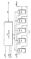
- Fig. 2 shows is a block diagram of the illustrative embodiment of the invention shown as pixel formatter 200 in Fig. 1.
- Eight-bit latches 210 , 220 , 230 , and 240 in the typical input mode, are respectively assigned to R, G, B, and USM data.
- Eight-bit latch 250 is used as a "remainder" latch to allow pairing of pixel values (when odd numbers of colors are to be captured) for writing into the FIFO buffer 120 (in Fig. 1), which, as explained in the discussion below of Fig. 5E, is organized into memory locations of two bytes or 16 bits.
- one mode of data transmission would be to latch the R and G data into latches 210 and 220 respectively, then the B and USM data into latches 230 and 240 respectively.
- the contents of latches 210 and 220 are then written to the FIFO buffer 120 (Fig. 1), while the contents of latch 230 are held for pairing with another pixel value. For example, if the R and G values for the next pixel scanned are latched into latches 210 and 220 respectively, the B value for that pixel is latched into the remainder latch 250 , keeping the B value for the previous pixel intact in latch 230 (the USM value in latch 240 may simply be overwritten).
- latch 230 The contents of latch 230 are then paired with the contents of latch 210 and written to FIFO buffer 120 (Fig. 1), followed by the contents of iatch 220 and remainder latch 250 to complete the cycle.
- FIFO buffer 120 Fig. 1
- only latches 210 and 220 are bi-directional, since only two pixel values were required in the particular output mode. Modes are selected on the four-bit line 215 , allowing for 16 modes. Input modes may include RGB (in sequence), R only, G only or B only. Output modes may include multiple images such as "one up,” “two up,”or “four up.”
- Fig. 3 is a block diagram of the state machine portion of the pixel formatter 200 .
- state defined as a set of values measured at selected parts of a circuit, such as the outputs
- a state machine is one which progresses through a sequence of states, with each transition to a new state determined by the current state plus other input conditions.
- the current state is defined at lines 345 , which are outputs of a state generator 330 , according to the mode selected on lines 215 .
- the condition code select signals on lines 325 through multiplexer 310 , select the signal on one of lines 305 as a condition code signal to appear on line 315 .
- Lines 305 further specified in Fig. 5A and discussed below, include transmission request and diagnostic signal lines.
- the condition code signal selected on iine 315 is synchronized by a D-type flip-flop 320 to be input on iine 330 , along with the present state on lines 340 , to the state generator 330 .
- a transition is or is not made to a new state, according to the present state, the condition code and the mode selected on lines 215 .
- the pixel formatter is strobed by a 20 MHz clock signal on line 225 in Figs.2, 3, 5A and 5B.
- the clock frequency is several times the frequency of pixel values arriving on the input/output data bus 235 , allowing for formatting without compromising the rate of data throughput. Operation at this speed is possible through the use, for example, of the simple state machine of the illustrative embodiment, implemented with registered PROMs for the state generator 330 and output decoder 340 (Fig. 3).
- the synchronization D-type flip-flop 320 is strobed by line 225 to pass a condition code signal on line 335 to the registered PROM state generator 330 synchronously with the clocking of the entire pixel formatter subsystem 200 (Fig. 1), including the state generator 330 and the output decoder 340 (Fig. 3).
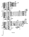
- the condition code 43 is used in conjunction with the 4-bit mode 41 set on lines 215 (Figs. 5A and 5B) and a six-bit state code 42 to determine an address 40 within the memory maps, exemplified by Fig. 4B, of the 2KX8 registered PROMs 330 , 340′ , 340 ⁇ , and 340′′′ used in the illustrative embodiment (Figs. 5A and 5B).
- the PROMs are easily programmable using standard techniques. The contents of a given memory location in PROM 330 , used as a state generator, directly specifies the current state.
- PROMs 340′ , 340 ⁇ , and 340′′′ used as output decoders, are used directly, bit-by-bit, as control signals. Thus, each clock pulse results in direct output, allowing for very high speed operation.
- registered PROM 330 is employed as a state generator, with the new state specified on the six outputs designated 511 .
- These six bits are connected to the inputs of the three decoder PROMs 340′ , 340 ⁇ , and 340′′′ (Fig. 5B) to address their contents, resulting in appropriate output signals respectively on lines 521 , 522 , and 523 .
- the six bits are also returned to the input of 330 to specify the present state, which, along with the mode selected on lines 215 and the condition code on line 335 , are the inputs for the generation of the next state.
- PROM 330 also has outputs 512 , which control the functions of the FIFO buffer 120 (Fig. 1), shown in further detail in Fig. 5E.
- the condition code is selected by the input multiplexer 310 from among eight inputs 502 according to the 3-bit condition code select signals on lines 501, which are outputs from output decoder 340′ .
- Inputs 502 include the device enable signal line 502′ and the request signal line 502 ⁇ .
- the device enable signal on line 502′ is set by the system software when initialization has taken place.
- the request signal on line 502 ⁇ is sent by the input/output device with each transmission of data.
- condition codes in the implemention shown in Fig. 5A include auxiliary requests on line 504′ , subline (for multiple separation outputs) start signals on line 504 , and diagnostic control signals on lines 506 . Again, these are selected by multiplexer 310 according to the condition code select signal 501 within an appropriate state sequence.
- Fig. 5A Also shown in Fig. 5A are the pull-up and pull-down lines 508 . Acknowledgement (used for asynchronous transmission) is made via lines 521′ and 504 .
- the master reset iine 507 is used to initialize the state generator 330 to state 0 and to select the device enable signal 502′ as the condition code input 315 at multiplexer 310 .
- Other lines on 504 to the input/output device are used to transmit data for diagnostics and the pixel counter used by the system to determine the size of the mask or cropping of the image (and thus the length of the scan).
- Output lines 522 and 523 from output decoders 340 ⁇ and 340′′′ respectively control latching on latches 210 , 220 , 230 , 240 , and 250 (Figs. 5C and 5D), and FIFO buffer 120 (Fig. 1).
- lines 522′ and 522 ⁇ strobe bidirectional latch 210 to latch data from data bus 265 and input/output data bus 235 , respectively, for data flow in opposite directions.
- the direction signal 506′ (Fig. 5C), originating in another portion of the drum scanner interface 110 (Fig 1), selects the direction of transmission from latch 210 .
- Line 522′′′ is used to raise the impedance of latch 210 to effectively take the latch off data buses 235 and 265 , and when negated, is used, with the direction signal 506 , to enable transmission in the selected direction.
- line 523′ is used to take latch 240 off data bus 265 and, when negated, enables transmission of the contents of latch 240 on data bus 265 .
- Line 202 in Fig. 5C is used for diagnostic purposes.
- Fig. 5E is a block diagram of the FIFO buffer used in the illustrative embodiment.
- a FIFO memory 380 of 32KB is organized into 16K addresses of 16 bits, allowing 16-bit parallel transfer on system bus 385 , which connects with other portions of the drum scanner interface 110 , such as disk drive 130 (Fig. 1).
- Two FIFO registers or latches are included, FIFO latch 350 corresponding to the high byte or 8 bits of a particular memory location and FIFO latch 360 for the low byte, which are read to and from memory 380 over lines 355 and 365 respectively upon command from FIFO controller 370 .
- the controller 370 responds to read and write signals on lines 512 ⁇ and 512′ respectively from the state generator 330 (Fig. 5A).
- FIFO latches 350 and 360 are clocked respectively by signals on lines 255′′′ and 255′ from PROM output decoder 340 ⁇ (Fig. 5B) to accept data from the 8-bit internal bus 265 .
- Lines 255 ⁇ ⁇ and 255 ⁇ when negated, respectively enable transmission of data from latches 350 and 360 over lines 355 and 365 to the FIFO memory 380 .
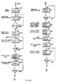
- Figs. 6A and 6B show a sample state sequence for input of R, G, and B data from input device 101 (Fig. 1).
- state 601 (S0) is the reset state, with condition code select code at lines 501 equal to 0 at multiplexer 310 , thereby selecting the device enable signal 502′ in Fig. 5A.
- State 601 results in state 602 (S1), selected at lines 511 at the state generator 330 (Fig. 5A) at the next clock pulse.
- State 602 and branch 603 form a loop waiting for the device enable signal 502′ .
- the condition code select signal on lines 501 switches to 1, selecting the data transfer request signal on line 502 ⁇ as the condition code.
- State 605 (S3) and branch 606 form a loop waiting for a request signal.
- state 607 latches the R and G data into latches 210 and 220 (Fig. 5D). Then state 608 (S5) and branch 609 form a loop waiting for the request to be negated. When that condition occurs, state 611 (S6) and branch 612 form a loop waiting for a request on line 502 ⁇ corresponding to the B value.
- state 613 latches the B value into latch 230 and puts the R value in latch 210 on bus 265 .
- State 614 (S8) latches the R value into FIFO latch 350 (Fig. 5E).
- State 615 (S9) initiates writing from FIFO latches 350 and 360 to the FIFO memory 380 (which is delayed and thereby captures the contents of latch 360 , which are subsequently latched in).
- State 616 (S10) puts the G value in latch 220 on bus 265 .
- State 617 (S11) latches the G value into the FIFO latch 360 (Fig. 5E) (and is captured by the FIFO write operation previously initi ated), and with branch 618 form a loop waiting for the request line 502 ⁇ to be negated.
- state 619 (S12) and branch 620 form a loop waiting for a request on line 502 ⁇ corresponding to the R and G values for a new pixel.
- state 621 (S13) latches the new R and G data into latches 210 and 220 (Fig. 5D) respectively and puts the B value for the previous pixel, still in latch 230 , on bus 265 .
- state 622 (S14) then latches the B value into the FIFO latch 350 .
- State 623 (S15) puts the new R value on bus 265 .
- State 624 latches the new R value into FIFO latch 360 , initiates writing from the FIFO latches 350 and 360 into the FIFO memory 380 , and with branch 625 form a loop waiting for the request to be negated.
- state 626 (S17) and branch 627 form a loop waiting for a request corresponding to the B value of the new pixel.
- state 628 latches the B value into the remainder latch 250 (Fig. 5D) and puts the G value on bus 265 .
- state 629 latches the G value into the FIFO latch 350 .
- State 630 (S20) initiates the delayed writing from latches 350 and 360 into the FIFO memory 380 .
- State 631 (S21) then puts the B value from the remainder latch (Fig. 5D) on bus 265 .
- state 632 latches the G value into the FIFO latch 360 , which is captured by the already initiated write into the FIFO memory and, with branch 633 , form a loop waiting for the request 502 ⁇ to be negated. The cycle is then repeated at state 605 (S3).
- the state generator 330 gives a FIFO read request on line 512 ⁇ , and the data is latched into FIFO latches 350 and 360 (Fig. 5E). Data is then put onto internal bus 265 one byte at a time and latched into latches 210 and 220 (Fig. 5D). The pixel formatter then enables the data onto the input/output bus 235 and acknowledges on line 521′ .
- test data from the system is put on the data bus 235 .
- the pixel formatter takes the test data and puts in onto the internal bus 265 one byte at a time through each of the latches 210 , 220 , 230 , 240 and 250 according to a diagnostic program.
- the test data is put into FIFO latches 350 and 360 and then a FIFO write request is given by the pixel formatter.
Landscapes
- Engineering & Computer Science (AREA)
- Multimedia (AREA)
- Signal Processing (AREA)
- Image Processing (AREA)
- Information Transfer Systems (AREA)
Applications Claiming Priority (2)
| Application Number | Priority Date | Filing Date | Title |
|---|---|---|---|
| US332343 | 1989-03-31 | ||
| US07/332,343 US4891709A (en) | 1989-03-31 | 1989-03-31 | Flexible formatting interface for pictorial data transfer |
Publications (2)
| Publication Number | Publication Date |
|---|---|
| EP0389748A2 true EP0389748A2 (de) | 1990-10-03 |
| EP0389748A3 EP0389748A3 (de) | 1991-01-23 |
Family
ID=23297804
Family Applications (1)
| Application Number | Title | Priority Date | Filing Date |
|---|---|---|---|
| EP19900101463 Withdrawn EP0389748A3 (de) | 1989-03-31 | 1990-01-25 | Flexibles Formatier-Interface zur Bilddatenübertragung |
Country Status (2)
| Country | Link |
|---|---|
| US (1) | US4891709A (de) |
| EP (1) | EP0389748A3 (de) |
Families Citing this family (9)
| Publication number | Priority date | Publication date | Assignee | Title |
|---|---|---|---|---|
| JP2651493B2 (ja) * | 1990-11-21 | 1997-09-10 | スターリング ドライ イメイジング,インコーポレイテッド | 印刷装置及び方法 |
| US5170261A (en) * | 1990-11-21 | 1992-12-08 | Polaroid Corporation | Printing method |
| US5481675A (en) * | 1992-05-12 | 1996-01-02 | International Business Machines Corporation | Asynchronous serial communication system for delaying with software dwell time a receiving computer's acknowledgement in order for the transmitting computer to see the acknowledgement |
| US5673403A (en) * | 1992-11-13 | 1997-09-30 | International Business Machines Corporation | Method and system for displaying applications of different operating systems on a single system using the user interface of the different operating systems |
| US5386518A (en) * | 1993-02-12 | 1995-01-31 | Hughes Aircraft Company | Reconfigurable computer interface and method |
| US5420696A (en) * | 1993-06-24 | 1995-05-30 | Xerox Corporation | Image data transfer architecture and method for an electronic reprographic machine |
| JP2003532698A (ja) * | 2000-05-10 | 2003-11-05 | プリンストン ユニバーシティ | 細菌の増殖および病理発生を調節するための化合物ならびに方法 |
| US7251752B2 (en) | 2001-10-01 | 2007-07-31 | Adams Phillip M | Computerized product improvement apparatus and method |
| US20050197860A1 (en) * | 2004-02-23 | 2005-09-08 | Rademr, Inc. | Data management system |
Family Cites Families (15)
| Publication number | Priority date | Publication date | Assignee | Title |
|---|---|---|---|---|
| US3603962A (en) * | 1970-03-18 | 1971-09-07 | Rca Corp | Color display for computer terminal |
| US4206457A (en) * | 1977-12-27 | 1980-06-03 | Rca Corporation | Color display using auxiliary memory for color information |
| US4425559A (en) * | 1980-06-02 | 1984-01-10 | Atari, Inc. | Method and apparatus for generating line segments and polygonal areas on a raster-type display |
| US4364037A (en) * | 1981-06-15 | 1982-12-14 | Cromemco Inc. | Transition data image processor |
| US4490797A (en) * | 1982-01-18 | 1984-12-25 | Honeywell Inc. | Method and apparatus for controlling the display of a computer generated raster graphic system |
| JPS60258589A (ja) * | 1984-06-06 | 1985-12-20 | 株式会社日立製作所 | 文字図形表示回路 |
| US4701790A (en) * | 1984-06-13 | 1987-10-20 | Dainippon Screen Manufacturing Co., Ltd. | Method and apparatus for color separation in an image reproduction scanner |
| GB8422208D0 (en) * | 1984-09-03 | 1984-10-10 | Crosfield Electronics Ltd | Colour printing data generation |
| US4814890A (en) * | 1984-11-19 | 1989-03-21 | Canon Kabushiki Kaisha | Image communicating system |
| JPS628193A (ja) * | 1985-07-04 | 1987-01-16 | インタ−ナショナル ビジネス マシ−ンズ コ−ポレ−ション | カラー画像表示装置 |
| JPH0785254B2 (ja) * | 1985-09-27 | 1995-09-13 | 株式会社東芝 | 文字画像読取装置 |
| US4817050A (en) * | 1985-11-22 | 1989-03-28 | Kabushiki Kaisha Toshiba | Database system |
| GB8614877D0 (en) * | 1986-06-18 | 1986-07-23 | Rca Corp | Display processors |
| WO1987007972A1 (en) * | 1986-06-18 | 1987-12-30 | Technology Inc. 64 | Display processor for use with a computer |
| US4763190A (en) * | 1986-06-30 | 1988-08-09 | Xerox Corporation | Digital color correction circuit |
-
1989
- 1989-03-31 US US07/332,343 patent/US4891709A/en not_active Expired - Fee Related
-
1990
- 1990-01-25 EP EP19900101463 patent/EP0389748A3/de not_active Withdrawn
Also Published As
| Publication number | Publication date |
|---|---|
| US4891709A (en) | 1990-01-02 |
| EP0389748A3 (de) | 1991-01-23 |
Similar Documents
| Publication | Publication Date | Title |
|---|---|---|
| EP0570146B1 (de) | Schnittstelle für ein Terminal zur Ausgabe von vollfarbigen Bildern | |
| US5303342A (en) | Method and apparatus for assembling a composite image from a plurality of data types | |
| US4196450A (en) | Selective copying apparatus | |
| US5113494A (en) | High speed raster image processor particularly suited for use in an image management system | |
| US5453845A (en) | Apparatus for providing variable gamma correction in both on-line and off-line modes of operation | |
| US7167266B2 (en) | Image memory apparatus | |
| EP0213189B1 (de) | Verfahren und vorrichtung zum adaptieren der auflösung von vorlagen | |
| US4891709A (en) | Flexible formatting interface for pictorial data transfer | |
| US5631983A (en) | Image forming system for synthesizing color image data with binary image data which has been colored with a predetermined color during the synthesizing operation | |
| EP0247751A2 (de) | Videoanzeigesystem mit einem graphischer Cursor | |
| US5602655A (en) | Image forming system for single bit image data | |
| US4967274A (en) | Image data conversion device | |
| JP3020957B2 (ja) | 画像処理方法 | |
| EP0336403B1 (de) | Bildlesegerät | |
| EP0346388B1 (de) | Hochgeschwindigkeits-rasterbildprozessor | |
| US20030044092A1 (en) | Method and apparatus for image data processing capable of performing a high speed processing using a risc and an AGP | |
| US5923901A (en) | System for transferring data in parallel to host computer using both of the rising and falling edges of host busy signals as transfer instruction signals | |
| JP3440117B2 (ja) | プリンタ制御装置 | |
| EP0276017B1 (de) | Einrichtung zur Hochgeschwindigkeitsverarbeitung gespeicherter Daten | |
| JPS61130996A (ja) | ビデオ入出力装置 | |
| JP3302010B2 (ja) | 電子機器の制御方法 | |
| JP3209996B2 (ja) | 画像処理システム | |
| JP3015039B2 (ja) | 画像処理システム | |
| KR930000995B1 (ko) | 그래픽 처리장치 | |
| JPS62145476A (ja) | 画像処理方式 |
Legal Events
| Date | Code | Title | Description |
|---|---|---|---|
| PUAI | Public reference made under article 153(3) epc to a published international application that has entered the european phase |
Free format text: ORIGINAL CODE: 0009012 |
|
| AK | Designated contracting states |
Kind code of ref document: A2 Designated state(s): DE FR GB |
|
| PUAL | Search report despatched |
Free format text: ORIGINAL CODE: 0009013 |
|
| AK | Designated contracting states |
Kind code of ref document: A3 Designated state(s): DE FR GB |
|
| RHK1 | Main classification (correction) |
Ipc: H04N 1/46 |
|
| 17P | Request for examination filed |
Effective date: 19910719 |
|
| 17Q | First examination report despatched |
Effective date: 19931028 |
|
| STAA | Information on the status of an ep patent application or granted ep patent |
Free format text: STATUS: THE APPLICATION IS DEEMED TO BE WITHDRAWN |
|
| 18D | Application deemed to be withdrawn |
Effective date: 19940308 |