EP0390183A2 - Circuit de séparation du signal de synchronisation - Google Patents
Circuit de séparation du signal de synchronisation Download PDFInfo
- Publication number
- EP0390183A2 EP0390183A2 EP90106144A EP90106144A EP0390183A2 EP 0390183 A2 EP0390183 A2 EP 0390183A2 EP 90106144 A EP90106144 A EP 90106144A EP 90106144 A EP90106144 A EP 90106144A EP 0390183 A2 EP0390183 A2 EP 0390183A2
- Authority
- EP
- European Patent Office
- Prior art keywords
- synchronizing signal
- signal
- inverting
- amplifying
- output
- Prior art date
- Legal status (The legal status is an assumption and is not a legal conclusion. Google has not performed a legal analysis and makes no representation as to the accuracy of the status listed.)
- Granted
Links
Images





Classifications
-
- H—ELECTRICITY
- H04—ELECTRIC COMMUNICATION TECHNIQUE
- H04N—PICTORIAL COMMUNICATION, e.g. TELEVISION
- H04N5/00—Details of television systems
- H04N5/04—Synchronising
- H04N5/08—Separation of synchronising signals from picture signals
Definitions
- the present invention relates generally to synchronizing signal separating circuits, and more particularly, to a synchronizing signal separating circuit for separating a synchronizing signal from a composite video signal in a circuit of, for example, a chrominance signal processing system, a deflection system or the like in a video apparatus such as a television (TV) receiver, a video tape recorder (VTR) and a video disc player.
- a synchronizing signal separating circuit for separating a synchronizing signal from a composite video signal in a circuit of, for example, a chrominance signal processing system, a deflection system or the like in a video apparatus such as a television (TV) receiver, a video tape recorder (VTR) and a video disc player.
- TV television
- VTR video tape recorder
- a horizontal synchronizing signal and a vertical synchronizing signal are separated from an inputted or reproduced composite video signal and supplied to various circuits, such as a chrominance signal processing circuit and a deflection circuit in the video apparatus.
- Fig. 1 is a circuit diagram showing one example of such a conventional synchronizing signal separating circuit, in case it is applied, for example, to a TV receiver. More specifically, a composite video signal received by an antennae and a video receiving circuit which are not shown is amplified in a video amplifying circuit 100 and then, supplied to a synchronizing signal separating circuit 200. The synchronizing signal separating circuit 200 extracts a horizontal synchronizing signal and a vertical synchronizing signal from the applied composite video signal and outputs the same as a composite synchronizing signal.
- the composite synchronizing signal outputted from the synchronizing signal separating circuit 200 is supplied, for example, to a deflection circuit 300, wherein the signal is further separated into a horizontal synchronizing signal and a vertical synchronizing signal for use in a deflecting operation.
- an output of the video amplifying circuit 100 is supplied to a positive input of a comparator 2 through a coupling condenser 1.
- a reference voltage of e.g. 2.5V is applied to a negative input of the comparator 2.
- An output of the comparator 2 after being inverted by an inverter 3, is supplied as a composite synchronizing signal to a deflection circuit 300, and also it is further inverted by an inverter 4 and then supplied to gates of a p-channel MOSFET 5 and an n-channel MOSFET 6.
- These MOSFETs and bias resistors 7 and 8 are connected in series between a power supply potential Vcc and a ground potential, and a node of the resistors 7 and 8 is further connected to the positive input of the comparator 2.
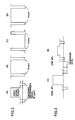
- Fig. 2 is a waveform diagram for explaining an operation of the synchronizing signal separating circuit 100 shown in Fig. 1, wherein Figs. 2 (A) (B), (C) and (D) show signal waveforms approximately in one horizontal period at the corresponding nodes A, B, C and D in the circuit of Fig. 1.
- the comparator 2 compares the composite video signal with the reference potential applied to the negative input (a dashed line of Fig. 2 (A)) and amplifies the result, and outputs a horizontal synchronizing signal of a negative polarity as shown in Fig. 2 (B) to supply the same to the inverter 3.
- the horizontal synchronizing signal inverted by the inverter 3 becomes a signal of a positive polarity as shown in Fig. 2 (C), and is supplied to the deflection circuit 300 in the succeeding stage and also supplied to the inverter 4 wherein it is further inverted.
- the inverter 4 outputs a horizontal synchronizing signal of the negative polarity as shown in Fig. 2 (D) and supplies the same to the gates of the p channel MOSFET 5 and n channel MOSFET 6.
- a ratio of a length of a horizontal synchronizing signal period to a length of the other period in one horizontal period is defined as about 1:12, and corresponding thereto, a ratio of a resistance value of the bias resistor 7 to that of the bias resistor 8 is set at about 12:1.
- the destination of thus separated horizontal synchronizing signal (Fig. 2 (C)) is not limited to the deflection circuit 300 shown in Fig. 1, but it can be supplied to any circuit requiring a synchronizing signal such as a chrominance signal processing circuit in the video apparatus.
- the inverters 3 and 4 are provided in case a horizontal synchronizing signal to be required is of the positive polarity, in case such a horizontal synchronizing signal of the negative polarity as shown in Fig. 2 (B) is required, they are not necessary, and it may be constituted so as to supply the output of the comparator 2 as a horizontal synchronizing signal.
- the horizontal synchronizing signal is separated in a manner as shown in Fig. 2, since a vertical synchronizing signal is comprised of a plurality of pulses each having the above described time ratio of 1:12, it can be separated in the circuit of Fig. 1 similarly to the horizontal synchronizing signal.
- the synchronizing signal separating circuit using MOSFETs is disclosed in, for example, Japanese Patent Laying Open Nos. 56-80965, 58-60880 and 61-198977.
- the coupling condenser 1 is charged with a fixed amount of electric charges from the power supply Vcc through the bias resistor 7 in the synchronizing signal period.
- an average picture level (APL) of a video signal becomes significantly different in each horizontal period in some cases.
- Fig. 3 (A) indicates that one horizontal line includes a lot of white portions to cause the APL to become high and Fig. (B) indicates that one horizontal line includes a lot of black portions to cause the APL to become low.
- the coupling condenser 1 is always charged with a fixed amount of electric charges with respect to video signals in horizontal periods in which the APLs thereof are different, a signal level supplied to the positive input of the comparator 1 falls or rises with respect to a fixed separation level (dashed line of Fig. 3) supplied to the negative input of the comparator 2.
- a separation level dashed line of Fig. 3
- noise, a burst signal or the like on the video signal is erroneously detected as a synchronizing signal in some cases and then outputted, so that various processings using a synchronizing signal can not be performed normally.
- an object of the present invention is to provide a synchronizing signal separating circuit capable of correctly separating a synchronizing signal from a composite video signal.
- Another object of the present invention is to provide a synchronizing signal separating circuit which does not erroneously detect noise, a burst signal or the like in a composite video signal as a synchronizing signal.
- a further object of the present invention is to provide a synchronizing signal separating circuit capable of maintaining a difference in level between a top level of a synchronizing signal and a separation level to be constant, irrespective of an APL of an inputted video signal.
- the present invention is a synchronizing signal separating circuit for separating a synchronizing signal from an inputted signal including at least a synchronizing signal
- the circuit comprises a coupling condenser for receiving an inputted signal, an inverter for inverting and amplifying the input signal received through the coupling condenser, a limiter for limiting an amplitude of an output signal of the inverter to supply the output signal having its amplitude limited as the synchronizing signal, a first bias resistor for connecting an output node to an input node of the inverter to charge the coupling condenser with an output signal of the inverter, a switch provided between the output node of the inverter and the first bias resistor and being controlled so as to be turned on in a synchronizing signal period in response to an output signal of the limiter, and a second bias resistor provided between the input node of the inverter and a ground potential for discharging electric charges of the coupling condenser.
- a principal advantage of the present invention is that even if a composite video signal having a different APL is inputted, a level difference between a top level of a synchronizing signal and a separation level does not change, whereby the synchronizing signal can be correctly separated.
- Fig. 4 is the circuit diagram showing the synchronizing signal separating circuit according to the first embodiment of the present invention.
- an output of a video amplifying circuit 100 is supplied to a synchronizing signal separating circuit 400, wherein it is supplied to an input of an inverter 12 through a coupling condenser 1.
- An output of the inverter 12 is supplied to an input of an inverter 13 and also supplied to an input node A of the inverter 12 through a switch 14 and a bias resistor 10 connected in series.
- the input node A is grounded through a bias resistor 11.
- An output of the inverter 13 is supplied as a composite synchronizing signal to a deflection circuit 300 and also supplied as a control signal to the switch 14 to control the switching of the switch 14.
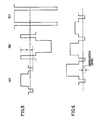
- Fig. 5 is the waveform diagram for explaining an operation of the synchronizing signal separating circuit 400 shown in Fig. 4, wherein Figs. 5 (A), (B) and (C) show signal waveforms approximately in one horizontal period at the corresponding nodes A, B and C in the circuit of Fig. 4, respectively.
- a dashed line in Fig. 5 indicates a threshold level of the inverters 12 and 13.
- the inverter 12 inverts and amplifies the composite video signal to output such a signal as shown in Fig. 5 (B) and then supplies the signal to the input of the inverter 13 and also to the input node A of the inverter 12 through the switch 14 and the bias resistor 10.
- the inverter 13 inverts and amplifies the supplied signal to output such a horizontal synchronizing signal of a negative polarity as shown in Fig. 5 (C) and then supplies the same to the deflection circuit 300.
- the inverter 13 functions as a limiter.
- the horizontal synchronizing signal outputted from the inverter 13 is supplied also to the control input of the switch 14.
- the switch 14 is constituted so as to be turned on while a control signal is at an "L" level and turned off while it is at an "H” level. Accordingly, in a horizontal synchronizing signal period (during an "L" level period of Fig. 5 (C)) the switch 14 is turned on, so that the coupling condenser 1 is charged with the amount of electric charges corresponding to a voltage indicated by V in Fig. 5 (B) through the bias resistor 10. On the other hand, in other period (“H" level period of Fig. 5 (C)) than the horizontal synchronizing signal period, the switch 14 is turned off, so that the electric charges stored in the coupling condenser 1 are discharged through the bias resistor 11.
- the coupling condenser 1 is charged with the amount of electric charges corresponding to the voltage V shown in Fig. 5 (B)
- the voltage V also fluctuates correspondingly. For example, if the separation level becomes contiguous to the lower end of the horizontal synchronizing signal, the voltage V becomes small and the amount of electric charges to be charged decreases, so that the separation level is shifted upward.
- the resistance value of the bias resistor 11 larger than that of the bias resistor 10 causes the separation level to near the lower end of the synchronizing signal.
- separation of the synchronizing signal becomes less susceptible to the video signal, thereby the separation sensitivity is improved.
- increased gain of the inverter 12 causes the voltage V to be increased, whereby the amount of electric charge to be charged is also increased. This also enables the separation level to near the lower end of the synchronizing signal to improve the separation sensitivity.
- Fig. 7 is the circuit diagram showing the synchronizing signal separating circuit according to the second embodiment of the present invention.
- a basic configuration of a synchronizing signal separating circuit 500 shown in Fig. 7 is the same as that of the synchronizing signal separating circuit 400 according to the first embodiment shown in Fig. 4 except for the following points. Namely, a comparator 15 is provided in place of the inverter 13, for comparing the output and the input of the inverter 12, the output of the inverter 12 is taken out through separately provided low pass filter (LPF) 16 and inverter 21, and series-connected bias resistor 23 and switch 22 are provided between the node A and the ground, in parallel with the bias resistor 11.
- LPF low pass filter
- the above described LPF 16 is comprised of an inverter 18, a condenser 19 and a resistor 20 and has an output supplied to a synchronization determining circuit (not shown) through the inverter 21.
- the output of the inverter 17 is supplied to a horizontal automatic frequency control (AFC) circuit for use as a chrominance signal processing circuit or the like.
- Switching of the switch 22 is controlled by a vertical equalizing pulse extracted in a vertical synchronizing signal separating circuit (not shown) provided in a stage subsequent to, for example, this synchronizing signal separating circuit.
- the inverters 24 and 17 may be suitably provided as required in order to obtain the synchronizing signal of the desired polarity.
- Fig. 8 is a waveform diagram for explaining an operation of the synchronizing signal separating circuit 500 shown in Fig. 7, wherein Figs. 8 (A), (B), (C) and (D) show signal waveforms approximately in one horizontal period at the corresponding nodes A, B, C and D in the circuit of Fig. 7, respectively.
- the inverter 12 inverts and amplifies the signal to output such a signal as shown in Fig. 8 (B) and then supplies the signal to a positive input of the comparator 15 and also to the input node A of the inverter 12 through the switch 14 and the bias resistor 10.
- the output of the inverter 12 is supplied also to the inverter 21 through the LPF 16.
- the signal of the node A (Fig. 8 (A)) is supplied to a negative input of the comparator 15, so that the comparator 15 outputs a horizontal synchronizing signal of the positive polarity shown in Fig.
- the switch 14 is a switch which is turned on during the control signal is at the "L" level and turned off during it is at the "H” level, as described above. Accordingly, in the horizontal synchronizing signal period (in the "L" level period of Fig.
- the direct current bias at the node A fluctuates in each horizontal period in response to an APL in the horizontal period, so that the level difference between the top level of the horizontal synchronizing signal and the separation level is always maintained to be constant, thereby making a correct separation of the synchronizing signal possible.
- the output of the inverter 12 (Fig. 8 (B)) is separately detected as a horizontal synchronizing signal through the LPF 16 and the inverter 21 functioning as a limiter and supplied to, for example, a synchronization determining circuit.
- LPF 16 between the inverters 12 and 21 is intended for the improvement of separation sensitivity in a weak electric field. More specifically, generally in the weak electric field, a synchronizing signal is covered with noise, and consequently if the synchronizing signal including such noise is directly supplied to a synchronization determining circuit in a succeeding stage, synchronization is erroneously determined to cause malfunction of a video apparatus. Therefore, by interposing such LPF 16 between the inverters 12 and 21, noise component is removed to prevent the malfunction in the weak electric field.
- the switch 22 is turned on by the vertical equalizing pulses extracted in the vertical synchronization separating circuit (not shown) in the succeeding stage.
- the separation level goes away from the top level of the synchronizing signal to improve the separation sensitivity, there is no possibility of erroneous separation of the synchronization signal because no video signal exists in the vertical blanking period.
- Fig. 9 is a circuit diagram showing a synchronizing signal separating circuit according to a third embodiment of the present invention.
- the embodiment shown in Fig. 9 comprises a first synchronizing signal separating circuit 600 for receiving a composite video signal to separate a composite synchronizing signal including a horizontal synchronizing signal and a vertical synchronizing signal, and a second synchronizing signal separating circuit 700 for receiving the composite synchronizing signal to separate only the vertical synchronizing signal.
- the first and the second synchronizing signal separating circuits 600 and 700 have the same structure as that of the synchronizing signal separating circuit 400 according to the first embodiment shown in Fig. 4 except for the following points.
- the first synchronizing signal separating circuit 600 is provided with an OR gate 36 for receiving a pseudo-horizontal synchronizing signal and a pseudo-vertical synchronizing signal, an AND gate 37 for receiving an output of the OR gate 36 and a synchronizing determining signal, an inverter 39 for inverting the output of the inverter 13, and an NOR gate 38 for receiving an output of the AND gate 37 and an output of the inverter 39, wherein an output of the NOR gate 38 is supplied as a control input to the switch 14.
- the above described synchronization determining signal is a signal supplied from a synchronization determining circuit (not shown), which attains the "H" level in the synchronization period and attains the "L" in the non-synchronization period.
- the pseudo-horizontal synchronizing signal and the pseudo-vertical synchronizing signal are obtained by frequency-dividing an oscillating output of a voltage controlled oscillator (VCO) in a horizontal AFC circuit
- the pseudo-horizontal synchronizing signal is a signal attaining the "H" level during a period having a length approximately equal to that of the horizontal synchronization period
- the pseudo-vertical synchronizing signal is that attaining the "H" level during a period having a length approximately equal to that of the vertical synchronization period.
- Fig. 10 is a block diagram showing such horizontal AFC circuit. Referring to Fig.
- a VCO 40, an LPF 41, a first frequency divider 42 and a phase comparator circuit 43 constitute an AFC loop, wherein an oscillating output of the VCO 40 oscillating at a frequency of a predetermined multiple of a horizontal frequency f H is frequency-divided by a predetermined frequency-dividing ratio in the first frequency divider 42 through the LPF 41 and then supplied to one input of the phase comparator circuit 43.
- a horizontal synchronizing signal separated by the synchronizing separating circuit 600 of Fig. 9 is supplied to the other input of the phase comparator circuit 43, wherein phases of both signals are compared.
- the phase comparator circuit 43 outputs an error output and supply the same to the VCO 40 to adjust an oscillating period of the VCO, such that the horizontal synchronizing signal and the oscillating output of the VCO 40 have a predetermined phase relation.
- an output of the first frequency divider 42 is taken out as a pseudo-horizontal synchronizing signal and supplied to the OR gate 36 of Fig. 9, and also supplied to the second frequency divider 44, which divider 44 frequency-divides the supplied pseudo-horizontal synchronizing signal to generate a pseudo-vertical synchronizing signal and supplies the same to the OR gate 36 of Fig. 9.
- the output of the inverter 13 is taken out as a composite synchronizing signal including a horizontal synchronizing signal and a vertical synchronizing signal and then supplied to the horizontal AFC circuit of Fig. 10, and also integrated by a LPF comprising a resistor 26 and a condenser 27 and then supplied to the second synchronizing signal separating circuit 700.
- the second synchronizing signal separating circuit 700 basically has the same structure as that of the synchronizing signal separating circuit 400 of Fig. 4, it is provided with series-connected bias resistor 30 and switch 31 arranged between an input node of an inverter 33 and a ground potential, in parallel with a bias resistor 29, similarly to the synchronizing signal separating circuit 500 of Fig. 7. Similar to the embodiment of Fig. 7, switching of the switch 31 is controlled by vertical equalizing pulses. An output of the inverter 35 is supplied as a vertical synchronizing signal to various signal processing systems.
- discharging of the coupling condenser 1 is performed in other period than a synchronizing signal period, in case the APL abruptly changes during the period, a composite video signal having different APL is inputted before the coupling condenser 1 is completely discharged, so that a top level of the synchronizing signal fluctuates with respect to the separation level, whereby it becomes impossible to separate the synchronizing signal correctly.
- the first synchronizing signal separating circuit 600 of Fig. 9 is made for resolving such problems, which is capable of correctly separating the synchronizing signal even if an APL fluctuates abruptly.
- Fig. 11 is a waveform diagram for explaining an operation of the first synchronizing signal separating circuit 600 of Fig. 9, wherein Figs. 11 (A1) and (A2) show signal waveforms at the node A and Figs. 11 (B1) and (B2) show signal waveforms at the node B.
- Figs. 11 (A1) show signal waveforms at the node A
- Figs. 11 (B1) and (B2) show signal waveforms at the node B.
- the switch 14 is turned on, so that the coupling condenser 1 is charged with the amount of the electric charges corresponding to a voltage V1 of Fig. 11 (B1).
- Fig. 12 is a timing chart showing a relation between the original composite video signal (A) and the pseudo-horizontal synchronizing signal (B).
- the pseudo-vertical synchronizing signal is also NOR-processed with the inverted output of the inverter 13 and supplied to the switch 14 as a control input, the switch 14 is turned on during a period having a length approximately equal to that of the original vertical synchronizing signal period, so that the coupling condenser 1 is discharged to maintain the relation between the separation level and the top level of the synchronizing signal to be constant even in case a vertical synchronizing signal in a composite video signal largely fluctuates due to, for example, AG characteristics of a tuner, abnormal electric wave or the like.
- the output of the inverter 13 is supplied as a composite synchronizing signal to the above described horizontal AFC circuit and also integrated by the LPF comprising the resistor 26 and the condenser 27 and then supplied to the second synchronizing signal separating circuit 700.
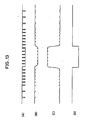
- Fig. 13 is a timing chart for explaining an operation of the second synchronizing signal separating circuit 700 of Fig. 9, wherein Fig. 13 (A) shows a signal waveform at the point C of Fig. 9, that is, a composite synchronizing signal comprising a horizontal synchronizing signal and a vertical synchronizing signal separated by the first synchronizing signal separating circuit 600.
- a composite synchronizing signal passes through the LPF comprising the resistor 26 and the condenser 27 to become a signal of such waveform as shown in Fig. 13 (B) at the point E of Fig. 9.
- This signal is inverted and amplified by the inverter 33 to becomes a signal of such waveform as shown in Fig. 13 (C) at the point F of Fig. 9.
- the signal is further inverted and amplified by the inverter 35, and at the point G of Fig. 9, only a vertical synchronizing signal is separated therefrom as shown in Fig. 13 (D) and which is supplied to the various circuits (
- the switches 31 is turned on in response to vertical equalizing pulses, and the bias resistor 30 is connected between the node E and the ground.
- the separation level rises with respect to the top level of the vertical synchronizing signal of Fig. 13 (B), so that the influence of the small pulses included in the top level can be eliminated, whereby separation sensitivity during the vertical synchronizing signal period can be improved.
- Figs. 14 and 15 show modified examples of the embodiment shown in Fig. 4, in which various types of electronic switches are employed as the switch 14. More specifically, Fig. 14 shows a case wherein a diode 51 is employed as the switch 14 of Fig. 4, and Fig. 15 shows a case wherein a transistor 52 is employed as the switch 14 of Fig. 4, and the same effect as that of the above described embodiment can be obtained in either cases.
Landscapes
- Engineering & Computer Science (AREA)
- Multimedia (AREA)
- Signal Processing (AREA)
- Synchronizing For Television (AREA)
Applications Claiming Priority (2)
| Application Number | Priority Date | Filing Date | Title |
|---|---|---|---|
| JP83129/89 | 1989-03-31 | ||
| JP8312989 | 1989-03-31 |
Publications (3)
| Publication Number | Publication Date |
|---|---|
| EP0390183A2 true EP0390183A2 (fr) | 1990-10-03 |
| EP0390183A3 EP0390183A3 (fr) | 1991-10-30 |
| EP0390183B1 EP0390183B1 (fr) | 1996-07-17 |
Family
ID=13793589
Family Applications (1)
| Application Number | Title | Priority Date | Filing Date |
|---|---|---|---|
| EP90106144A Expired - Lifetime EP0390183B1 (fr) | 1989-03-31 | 1990-03-30 | Circuit de séparation du signal de synchronisation |
Country Status (4)
| Country | Link |
|---|---|
| EP (1) | EP0390183B1 (fr) |
| KR (1) | KR0144350B1 (fr) |
| CA (1) | CA2013532C (fr) |
| DE (1) | DE69027802T2 (fr) |
Cited By (1)
| Publication number | Priority date | Publication date | Assignee | Title |
|---|---|---|---|---|
| EP0559016A3 (en) * | 1992-03-02 | 1993-11-10 | Thomson Consumer Electronics | Sync separator |
Family Cites Families (2)
| Publication number | Priority date | Publication date | Assignee | Title |
|---|---|---|---|---|
| DE3444764A1 (de) * | 1984-12-07 | 1986-06-12 | Siemens AG, 1000 Berlin und 8000 München | Impulsabtrennschaltung fuer videosignale |
| FR2595528B1 (fr) * | 1986-03-05 | 1988-05-13 | Thomson Csf | Dispositif de separation des impulsions de synchronisation d'un signal de television |
-
1990
- 1990-03-30 DE DE69027802T patent/DE69027802T2/de not_active Expired - Lifetime
- 1990-03-30 KR KR1019900004288A patent/KR0144350B1/ko not_active Expired - Fee Related
- 1990-03-30 CA CA002013532A patent/CA2013532C/fr not_active Expired - Lifetime
- 1990-03-30 EP EP90106144A patent/EP0390183B1/fr not_active Expired - Lifetime
Cited By (2)
| Publication number | Priority date | Publication date | Assignee | Title |
|---|---|---|---|---|
| EP0559016A3 (en) * | 1992-03-02 | 1993-11-10 | Thomson Consumer Electronics | Sync separator |
| TR26558A (tr) * | 1992-03-02 | 1995-03-15 | Thomson Consumer Electronics | Video gösterim aygitina mahsus senk ayirma cihazi. |
Also Published As
| Publication number | Publication date |
|---|---|
| KR0144350B1 (ko) | 1998-07-15 |
| DE69027802T2 (de) | 1997-02-27 |
| DE69027802D1 (de) | 1996-08-22 |
| CA2013532A1 (fr) | 1990-09-30 |
| EP0390183B1 (fr) | 1996-07-17 |
| KR900015523A (ko) | 1990-10-27 |
| EP0390183A3 (fr) | 1991-10-30 |
| CA2013532C (fr) | 2000-02-01 |
Similar Documents
| Publication | Publication Date | Title |
|---|---|---|
| US5517249A (en) | Auxiliary video data slicer with adaptive slicing level capability | |
| US5280356A (en) | Clamp circuit for clamping video signal including synchronizing signal at a prescribed potential | |
| EP0067822B1 (fr) | Sous-systeme de recepteur de television a circuits integres monoplaquettes, a grande echelle | |
| EP0660611B1 (fr) | Circuit de récupération d'horloge pour un signal vidéo numérique sériel | |
| US4942472A (en) | Detection circuit for a video tape recorder signal | |
| JPH03117995A (ja) | 色信号輪郭補正装置 | |
| US4999707A (en) | Synchronizing signal separating circuit separating synchronizing signal from a composite video signal | |
| US5784122A (en) | Chroma lock detector | |
| US4543614A (en) | Video sync validity detector | |
| CA2013532C (fr) | Circuit de separation de signaux de synchronisation | |
| EP0756799B1 (fr) | Dispositif servant a deriver un signal d'horloge a partir d'un signal de synchronisation et enregistreur video muni de ce dispositif | |
| US4682087A (en) | Apparatus for controlling amplitude of vertical deflection signal | |
| US4148068A (en) | Television synchronizing signal separating circuit | |
| US2906818A (en) | Transistor phase detector circuit | |
| US4882624A (en) | Synchronizing signal separation circuit for a television receiver | |
| JP3439143B2 (ja) | 水平同期回路 | |
| US5287170A (en) | Broadcasting signal detecting circuit for SECAM and PAL signal formats | |
| JP3456712B2 (ja) | 複合映像信号検出回路 | |
| KR0115245Y1 (ko) | Pal/secam방식 방송신호 판별회로 | |
| US7023489B2 (en) | Method and device for detecting the parity of successive fields of an interlaced video signal | |
| EP0487072A2 (fr) | Générateur de signal de déflection verticale | |
| US5982451A (en) | Video signal level detector | |
| JPH06338786A (ja) | マイクロコンピュータ | |
| JPS62250773A (ja) | 一致回路 | |
| JP3239437B2 (ja) | 水平同期信号検出回路 |
Legal Events
| Date | Code | Title | Description |
|---|---|---|---|
| PUAI | Public reference made under article 153(3) epc to a published international application that has entered the european phase |
Free format text: ORIGINAL CODE: 0009012 |
|
| AK | Designated contracting states |
Kind code of ref document: A2 Designated state(s): DE ES FR GB IT |
|
| 17P | Request for examination filed |
Effective date: 19901228 |
|
| PUAL | Search report despatched |
Free format text: ORIGINAL CODE: 0009013 |
|
| AK | Designated contracting states |
Kind code of ref document: A3 Designated state(s): DE ES FR GB IT |
|
| 17Q | First examination report despatched |
Effective date: 19940328 |
|
| GRAG | Despatch of communication of intention to grant |
Free format text: ORIGINAL CODE: EPIDOS AGRA |
|
| GRAH | Despatch of communication of intention to grant a patent |
Free format text: ORIGINAL CODE: EPIDOS IGRA |
|
| GRAH | Despatch of communication of intention to grant a patent |
Free format text: ORIGINAL CODE: EPIDOS IGRA |
|
| GRAA | (expected) grant |
Free format text: ORIGINAL CODE: 0009210 |
|
| AK | Designated contracting states |
Kind code of ref document: B1 Designated state(s): DE ES FR GB IT |
|
| PG25 | Lapsed in a contracting state [announced via postgrant information from national office to epo] |
Ref country code: IT Free format text: LAPSE BECAUSE OF FAILURE TO SUBMIT A TRANSLATION OF THE DESCRIPTION OR TO PAY THE FEE WITHIN THE PRE;WARNING: LAPSES OF ITALIAN PATENTS WITH EFFECTIVE DATE BEFORE 2007 MAY HAVE OCCURRED AT ANY TIME BEFORE 2007. THE CORRECT EFFECTIVE DATE MAY BE DIFFERENT FROM THE ONE RECORDED.SCRIBED TIME-LIMIT Effective date: 19960717 Ref country code: ES Free format text: THE PATENT HAS BEEN ANNULLED BY A DECISION OF A NATIONAL AUTHORITY Effective date: 19960717 |
|
| ET | Fr: translation filed | ||
| REF | Corresponds to: |
Ref document number: 69027802 Country of ref document: DE Date of ref document: 19960822 |
|
| PLBE | No opposition filed within time limit |
Free format text: ORIGINAL CODE: 0009261 |
|
| STAA | Information on the status of an ep patent application or granted ep patent |
Free format text: STATUS: NO OPPOSITION FILED WITHIN TIME LIMIT |
|
| 26N | No opposition filed | ||
| REG | Reference to a national code |
Ref country code: GB Ref legal event code: IF02 |
|
| PGFP | Annual fee paid to national office [announced via postgrant information from national office to epo] |
Ref country code: GB Payment date: 20090325 Year of fee payment: 20 |
|
| PGFP | Annual fee paid to national office [announced via postgrant information from national office to epo] |
Ref country code: DE Payment date: 20090327 Year of fee payment: 20 |
|
| PGFP | Annual fee paid to national office [announced via postgrant information from national office to epo] |
Ref country code: FR Payment date: 20090316 Year of fee payment: 20 |
|
| REG | Reference to a national code |
Ref country code: GB Ref legal event code: PE20 Expiry date: 20100329 |
|
| PG25 | Lapsed in a contracting state [announced via postgrant information from national office to epo] |
Ref country code: GB Free format text: LAPSE BECAUSE OF EXPIRATION OF PROTECTION Effective date: 20100329 |
|
| PG25 | Lapsed in a contracting state [announced via postgrant information from national office to epo] |
Ref country code: DE Free format text: LAPSE BECAUSE OF EXPIRATION OF PROTECTION Effective date: 20100330 |