EP0390509B1 - Halbleiterbauelement und Verfahren zu dessen Herstellung - Google Patents
Halbleiterbauelement und Verfahren zu dessen Herstellung Download PDFInfo
- Publication number
- EP0390509B1 EP0390509B1 EP90303269A EP90303269A EP0390509B1 EP 0390509 B1 EP0390509 B1 EP 0390509B1 EP 90303269 A EP90303269 A EP 90303269A EP 90303269 A EP90303269 A EP 90303269A EP 0390509 B1 EP0390509 B1 EP 0390509B1
- Authority
- EP
- European Patent Office
- Prior art keywords
- conductive layer
- semi
- film
- ion
- gate electrode
- Prior art date
- Legal status (The legal status is an assumption and is not a legal conclusion. Google has not performed a legal analysis and makes no representation as to the accuracy of the status listed.)
- Expired - Lifetime
Links
Images


Classifications
-
- H—ELECTRICITY
- H10—SEMICONDUCTOR DEVICES; ELECTRIC SOLID-STATE DEVICES NOT OTHERWISE PROVIDED FOR
- H10D—INORGANIC ELECTRIC SEMICONDUCTOR DEVICES
- H10D30/00—Field-effect transistors [FET]
- H10D30/01—Manufacture or treatment
- H10D30/021—Manufacture or treatment of FETs having insulated gates [IGFET]
- H10D30/0223—Manufacture or treatment of FETs having insulated gates [IGFET] having source and drain regions or source and drain extensions self-aligned to sides of the gate
- H10D30/0227—Manufacture or treatment of FETs having insulated gates [IGFET] having source and drain regions or source and drain extensions self-aligned to sides of the gate having both lightly-doped source and drain extensions and source and drain regions self-aligned to the sides of the gate, e.g. lightly-doped drain [LDD] MOSFET or double-diffused drain [DDD] MOSFET
-
- H—ELECTRICITY
- H10—SEMICONDUCTOR DEVICES; ELECTRIC SOLID-STATE DEVICES NOT OTHERWISE PROVIDED FOR
- H10D—INORGANIC ELECTRIC SEMICONDUCTOR DEVICES
- H10D30/00—Field-effect transistors [FET]
- H10D30/60—Insulated-gate field-effect transistors [IGFET]
- H10D30/601—Insulated-gate field-effect transistors [IGFET] having lightly-doped drain or source extensions, e.g. LDD IGFETs or DDD IGFETs
- H10D30/605—Insulated-gate field-effect transistors [IGFET] having lightly-doped drain or source extensions, e.g. LDD IGFETs or DDD IGFETs having significant overlap between the lightly-doped extensions and the gate electrode
-
- H—ELECTRICITY
- H10—SEMICONDUCTOR DEVICES; ELECTRIC SOLID-STATE DEVICES NOT OTHERWISE PROVIDED FOR
- H10D—INORGANIC ELECTRIC SEMICONDUCTOR DEVICES
- H10D64/00—Electrodes of devices having potential barriers
- H10D64/01—Manufacture or treatment
- H10D64/013—Manufacture or treatment of electrodes having a conductor capacitively coupled to a semiconductor by an insulator
- H10D64/01302—Manufacture or treatment of electrodes having a conductor capacitively coupled to a semiconductor by an insulator the insulator being formed after the semiconductor body, the semiconductor being silicon
- H10D64/01304—Manufacture or treatment of electrodes having a conductor capacitively coupled to a semiconductor by an insulator the insulator being formed after the semiconductor body, the semiconductor being silicon characterised by the conductor
- H10D64/01306—Manufacture or treatment of electrodes having a conductor capacitively coupled to a semiconductor by an insulator the insulator being formed after the semiconductor body, the semiconductor being silicon characterised by the conductor the conductor comprising a layer of silicon contacting the insulator, e.g. polysilicon
- H10D64/01308—Manufacture or treatment of electrodes having a conductor capacitively coupled to a semiconductor by an insulator the insulator being formed after the semiconductor body, the semiconductor being silicon characterised by the conductor the conductor comprising a layer of silicon contacting the insulator, e.g. polysilicon the conductor further comprising a non-elemental silicon additional conductive layer, e.g. a metal silicide layer formed by the reaction of silicon with an implanted metal
- H10D64/0131—Manufacture or treatment of electrodes having a conductor capacitively coupled to a semiconductor by an insulator the insulator being formed after the semiconductor body, the semiconductor being silicon characterised by the conductor the conductor comprising a layer of silicon contacting the insulator, e.g. polysilicon the conductor further comprising a non-elemental silicon additional conductive layer, e.g. a metal silicide layer formed by the reaction of silicon with an implanted metal the additional conductive layer comprising a silicide layer formed by the silicidation reaction between the layer of silicon with a metal layer which is not formed by metal implantation
-
- H—ELECTRICITY
- H10—SEMICONDUCTOR DEVICES; ELECTRIC SOLID-STATE DEVICES NOT OTHERWISE PROVIDED FOR
- H10D—INORGANIC ELECTRIC SEMICONDUCTOR DEVICES
- H10D64/00—Electrodes of devices having potential barriers
- H10D64/01—Manufacture or treatment
- H10D64/013—Manufacture or treatment of electrodes having a conductor capacitively coupled to a semiconductor by an insulator
- H10D64/01302—Manufacture or treatment of electrodes having a conductor capacitively coupled to a semiconductor by an insulator the insulator being formed after the semiconductor body, the semiconductor being silicon
- H10D64/01304—Manufacture or treatment of electrodes having a conductor capacitively coupled to a semiconductor by an insulator the insulator being formed after the semiconductor body, the semiconductor being silicon characterised by the conductor
- H10D64/01324—Manufacture or treatment of electrodes having a conductor capacitively coupled to a semiconductor by an insulator the insulator being formed after the semiconductor body, the semiconductor being silicon characterised by the conductor characterised by the sectional shape, e.g. T or inverted-T
Definitions
- the present invention is directed to a semi-conductor device; and to a method of manufacturing such a device.
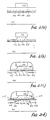
- a semi-conductor device produced by this method comprises a p-type semi-conductor substrate 201, a gate oxide film 202, a polysilicon film 203, a natural oxide film 204, a polysilicon film 205, a silicon oxide film 206, an n-type impurity layer 207 having low concentration, an insulating side wall 208 in the form of an oxide film, an n-type impurity layer 209 having a high concentration, and an oxide film 210.
- the polysilicon films 203, 205 constitute a gate electrode, and the impurity layers 207, 209 constitute source/drain regions.
- the p-type semi-conductor substrate 201 undergoes thermal oxidisation to form the gate oxide film 202.
- the polysilicon film 203 is deposited as a thin layer by the CVD method and the vapour is thereafter left in the air, thus forming the natural oxide film 204 to a thickness of 5.10 -10 m to 10.10 -10 m (5 ⁇ to 10 ⁇ ).
- the polysilicon film 205 and the silicon oxide film 206 are sequentially deposited by the CVD method. As illustrated in Figure 2(a), unnecessary portions of the silicon oxide film 206 are eliminated by photoetching.
- Dry etching is then effected with the oxide film 206 serving as a mask, thereby removing the unnecessary portions of the polysilicon film 205 as shown in Figure 2(b).
- the n-type impurity layer 207 is formed by ion implantation of an n-type impurity, ie. phosphorus, using the silicon oxide film 206 and the polysilicon film 205 as a mask, as illustrated in Figure 2(c).
- the side wall insulating film 208 is formed by first depositing silicon oxide film by the CVD method and then dry etching.
- oxidisation is carried out at 800°C in a wet atmosphere, to form the oxide film 210.
- the n-type impurity layer 209 is formed by effecting ion implantation on an n-type impurity, viz. arsenic, with the polysilicon film 203, oxide film 206 and side wall insulating film 208 serving as a mask.
- the oxide film 206 when depositing the silicon oxide film 208 by the CVD method, the oxide film 206 over-hangs the polysilicon film 205, and hence, as illustrated in Figure 3, it is hard for the silicon oxide film 208 to cover this region, resulting in the formation of voids. This leads to a deterioration in moisture resistance of the MOS transistor.
- the prior art described above also presents additional problems.
- the combined thickness of the films disposed on the channel region - ie. the gate oxide film 202, the polysilicon film 203, the natural oxide film 204, the polysilicon film 205 and the silicon oxide film 206 - amount to a large step. Consequently, a metallisation layer formed on the gate electrode for lead purposes is in some cases disrupted or disconnected due to the size of the above mentioned step; or alternatively the metallisation layer is short circuited because portions of the layer remain unetched when forming the layer on the gate electrode.
- IBM Technical Disclosure Bulletin, Vol. 24, No. 8, January 1982 pgs 4186 - 4187 disclose a method of manufacturing a semi-conductor device in which gate electrode layers are provided, source drain regions are then formed by ion implantation, and thereafter the device is subjected to an oxidation and drive in step.
- the present invention seeks to overcome the above problems.
- a method of manufacturing a semi-conductor device comprising:
- the method of manufacturing a semi-conductor device comprises the steps of: forming a first insulating film on a first conductivity type semi-conductor substrate; forming a first conductive film on the first insulating film; sequentially forming a second conductive film on the first conductive film; forming a MOS transistor gate electrode by use of the first and second conductive films; effecting thermal annealing thereon; performing ion implantation of first impurities of a second conductivity type into the semi-conductor substrate with the gate electrode serving as a mask; forming a side wall insulating film on the gate electrode by use of a second insulating film by effecting an isotropic ion etching after forming the second insulating film on the gate electrode as well as on the semi-conductor substrate; and introducing second impurities of the second conductivity type preferably using ion implantation with the gate electrode and the side wall insulating film serving as a mask.
- the kind of ions implanted and the ion implantation acceleration energy may be so set that the ions cannot pass through the combined thickness of the first and second conductive films but can pass through the thickness of the first conductive film alone.
- the depth of a region of the second ion implanted impurities of the second conductivity type is less than that of a region of the first ion implanted impurities of the second conductivity type.
- the first conductive film is a polysilicon film
- the second conductive film is a refractory metal film or a refractory metal silicide film.
- a first conductivity type semi-conductor substrate or p-type silicon substrate 101 doped with boron is oxidised at 1000°C in an oxidative atmosphere, thereby forming a gate oxide film 102 having a thickness of 150.10 -10 m (150 ⁇ ).
- a polysilicon film 103 is deposited up to a thickness of 1000.10 -10 m to 3000.10 -10 m (1000 ⁇ to 3000 ⁇ ) by the CVD method, and phosphorus is added as dopant to a level of more than 10 19 cm -3 by thermal diffusion.
- a refractory metal film, in this instance a molybdenum film, 104 is formed to a thickness of 1500.10 -10 m to 4000.10 -10 m (1500 ⁇ to 4000 ⁇ ) by sputtering.
- the molybdenum may be replaced by another refractory metal such as tungsten, tantalum or titanium and in these cases typical rates of volume reduction are as follows: tungsten silicide (WSi 2 ) 27%; tantalum silicide (TaSi 2 ) 25%; and titanium silicide (TiSi 2 ) 23%.
- tungsten silicide WSi 2
- TaSi 2 tantalum silicide
- TiSi 2 titanium silicide
- the degree of contraction as a total on both sides of the gate electrode, ranges from 0.05 ⁇ m to 0.2 ⁇ m on the assumption that gate length after etching the MOS transistor is 0.8 ⁇ m.
- the dimension of the molybdenum silicide film 105 disposed on the polysilicon film 103 after effecting thermal annealing is from 0.6 ⁇ m to 0.75 ⁇ m.
- the amount of contraction can readily be controlled with high accuracy, simply by changing the thicknesses of the polysilicon film 103 and the molybdenum film 104, and also the thermal annealing temperature after forming the gate electrode.
- ion implantation of n-type impurities in this instance phosphorus is carried out under conditions of an accelerating voltage set to be from 80 KeV to 200 KeV, and a dose set to be from 5 x 10 12 cm -2 to 5 x 10 14 cm -2 .
- the phosphorus is not implanted into the silicon substrate underneath the portion of the gate electrode composed of the polysilicon film 103 and the molybdenum silicide film 105, whereas the phosphorus is implanted shallowly into the silicon substrate under the portion of the gate electrode composed of the polysilicon film 103 in the region where the molybdenum silicide film 105 has contracted.
- the phosphorus is implanted deeply into the silicon substrate in the source/drain regions in which no gate electrode exists, thereby forming an n-type impurity layer 106 having a low impurity concentration as shown in Figure 1 (d).
- an isotropic etching is effected such that the length of the gate electrode of the MOS transistor comes to 0.8 ⁇ m; and thermal annealing is performed at 1000°C, thereby forming the molybdenum silicide film 105.
- the molybdenum silicide film contracts bilaterally by 0.1 ⁇ m on both sides, whereby the length thereof becomes approximately 0.6 ⁇ m.
- the ion implantation of the phosphorus is effected, the accelerating voltage being set to 160 KeV, and the dose being set to be 3 x 10 13 cm -2 .
- the phosphorus is not implanted into a channel region of the silicon substrate provided beneath the portion of the gate electrode consisting of the polysilicon film 103 and of the molybdenum silicide film 105, whereas the phosphorus is implanted shallowly into the silicon substrate under the portion of the gate electrode consisting of the polysilicon film 103 alone in the area where the molybdenum silicide film has contracted.
- a junction depth A is approximately 0.2 ⁇ m; a peak depth of the impurity concentration distribution of phosphorus is about 0.05 ⁇ m; and the concentration thereof is nearly 1 x 10 18 cm -3 .
- the phosphorus is implanted deep into the silicon substrate.
- a junction depth B is approximately 0.4 ⁇ m; a peak depth of the impurity concentration distribution of phosphorus is about 0.25 ⁇ m; and the concentration thereof is nearly 1 x 10 18 cm -3 . It is additionally stated that such data on the profile of the impurity is obtained after effecting annealing at 950°C for twenty minutes.
- a silicon oxide film is deposited to a thickness of 4000 ⁇ to 8000 ⁇ on the gate electrode as well as on the silicon substrate by the CVD method, and thereafter reactive ion etching is carried out to form a side wall oxide film 107.
- n-type impurities e.g. arsenic in this embodiment
- a dose set to be 1 x 10 15 cm -2 to 1 x 10 16 cm -2 is performed under conditions of an accelerating voltage set to be 50 KeV to 150 KeV, and a dose set to be 1 x 10 15 cm -2 to 1 x 10 16 cm -2 ; and thermal annealing is then effected at 900°C to 1000°C, thereby forming an n-type impurity layer 108 having a high impurity concentration.
- the n-type impurity layer 108 may be formed likewise without shaping the side wall oxide film 107.
- the MOS transistor constructed in accordance with the above described steps have a gate electrode, in which the polysilicon film 103 overlaps the n-type impurity layer 106 having a low concentration, and hence, if a voltage is impressed on the gate, an apparent resistance of the low concentration n-type impurity layer 106 is reduced due to its electric field. On the other hand, a crosswise electric field within the low concentration n-type impurity layer 106 is relieved. This results in an increment in drain current of the transistor, and it is therefore possible to avoid a deterioration of conductance associated with hot carriers.
- the properties of the MOS transistor largely vary depending on the overlap of the polysilicon film 103 of the gate electrode and the low concentration n-type impurity layer 106, but this can be controlled with high accuracy and facility simply by changing the thicknesses of the polysilicon film 103 and of the molybdenum film 104 and also the thermal annealing temperature after forming the gate electrode. Hence, scatter in the properties of the MOS transistor is reduced.
- the film thickness on the channel region is merely the sum of the thicknesses of the gate oxide film 102, the polysilicon film 103, and the molybdenum silicide film 105.
- a metallisation layer may be formed on the gate electrode to traverse the gate electrode without resulting in a short circuit due to portions of the metal remaining unetched when forming the metallisation layer on the gate electrode.
- the refractory metal film 104 disposed on the polysilicon film 103 comprises molybdenum.
- the same effects can, however, be expected by employing tungsten, titanium, platinum, cobalt, nickel and tantalum; and refractory metal silicide films thereof may also be used.
- the embodiment given above features a case where phosphorus is employed as the n-type impurity for the low concentration n-type impurity layer 106.
- the impurity may, however, include arsenic and antimony; and it may be provided by a combination of these impurities, e.g. phosphorus and arsenic.
- arsenic is employed as the n-type impurity for the high concentration n-type impurity layer 108.
- phosphorus and antimony are likewise available; and combinations of impurities may be used.
- boron is employed as the impurity for the p-type semi-conductor substrate, but gallium, aluminium and indium may also be used.
- the drain current of the MOS transistor increases, and it is possible to avoid a deterioration of conductance which is due to the hot carriers.
- a high speed and highly reliable MOS transistor can be provided.
- the moisture resistance of the MOS transistor is not diminished.
- the present invention as described exhibits the additional advantage of minimising the likelihood of short circuit and disruption of the metallisation layer on the gate electrode.
- the present invention may provide a semi-conductor device in which there is no short circuit or disruption of a metallisation layer formed on a gate electrode, which exhibits less scatter in the properties of the transistor and which has good moisture resistance.
- the invention may thus provide a high speed semi-conductor device having a high quality, high reliability and high yield.
- the invention may also be applied to a MIS type semi-conductor device.
Landscapes
- Insulated Gate Type Field-Effect Transistor (AREA)
- Electrodes Of Semiconductors (AREA)
- Junction Field-Effect Transistors (AREA)
Claims (6)
- Verfahren zum Herstellen eines Halbleiterbauelements, umfassend:dadurch gekennzeichnet, daß zwischen den Schritten (b) und (c) ein Tempern durchgeführt wird, um die zweite leitfähige Schicht relativ zur ersten leitfähigen Schicht zu schrumpfen.a) Bereitstellen eines Halbleitersubstrats (101) eines ersten Leitfähigkeitstyps;b) Bilden einer Gateelektrode auf dem Halbleitersubstrat, umfassend eine erste leitfähige Schicht (103) und eine hierauf angeordnete zweite leitfähige Schicht (105), wobei die erste leitfähige Schicht (103) ein Polysiliziummaterial umfaßt und die zweite leitfähige Schicht ein hitzefestes Metall umfaßt;c) lonenimplantieren von Fremdatomen eines zweiten Leitfähigkeitstyps in das Halbleitersubstrat, um unter Verwendung der ersten und der zweiten leitfähigen Schicht als eine Maske Source/Drain-Bereiche zu bilden; und
- Verfahren nach Anspruch 1, dadurch gekennzeichnet, daß die zweite leitfähige Schicht Molybdän ist und daß das Tempern bei einer Temperatur zwischen 850°C und 1100°C durchgeführt wird.
- Verfahren nach Anspruch 1 oder 2, dadurch gekennzeichnet, daß die zweite leitfähige Schicht reagiert, um während des Temperns ein hitzefestes-Metall-Silizid zu erzeugen.
- Verfahren nach einem der Ansprüche 1 bis 3, dadurch gekennzeichnet, daß der Schritt des lonenimplantierens unter Verwendung der ersten und zweiten leitfähigen Schicht als eine Maske die Wahl der Art von lonen und das Einstellen der lonenimplantations-Beschleunigungsenergie derart umfaßt, daß lonen durch die erste leitfähige Schicht, nicht aber durch sowohl die erste als auch die zweite leitfähige Schicht, durchgelassen werden.
- Verfahren nach einem der vorangehenden Ansprüche, dadurch gekennzeichnet, daß der Schritt des lonenimplantierens unter Verwendung der ersten und der zweiten leitfähigen Schicht als eine Maske dazu ausgelegt ist, eine erste ionenimplantierte Region geringerer Tiefe unterhalb eines Randabschnitts der ersten leitfähigen Schicht sowie eine zweite ionenimplantierte Region größerer Tiefe jenseits der ersten leitfähigen Schicht zu erzeugen.
- Verfahren nach einem der vorangehenden Ansprüche, dadurch gekennzeichnet, daß der Schritt des Bildens von Source/Drain-Bereichen das Bilden eines isolierenden Seitenwandfilms (107) auf der ersten und der zweiten leitfähigen Schicht sowie das lonenimplantieren von Fremdatomen des zweiten Typs unter Verwendung der ersten und der zweiten leitfähigen Schicht und des isolierenden Seitenwandfilms als eine Maske umfaßt.
Applications Claiming Priority (6)
| Application Number | Priority Date | Filing Date | Title |
|---|---|---|---|
| JP7610989 | 1989-03-28 | ||
| JP76109/89 | 1989-03-28 | ||
| JP7610889 | 1989-03-28 | ||
| JP76108/89 | 1989-03-28 | ||
| JP38757/90 | 1990-02-20 | ||
| JP2038757A JP2926833B2 (ja) | 1989-03-28 | 1990-02-20 | 半導体装置の製造方法 |
Publications (3)
| Publication Number | Publication Date |
|---|---|
| EP0390509A2 EP0390509A2 (de) | 1990-10-03 |
| EP0390509A3 EP0390509A3 (de) | 1990-11-22 |
| EP0390509B1 true EP0390509B1 (de) | 1998-07-01 |
Family
ID=27289931
Family Applications (1)
| Application Number | Title | Priority Date | Filing Date |
|---|---|---|---|
| EP90303269A Expired - Lifetime EP0390509B1 (de) | 1989-03-28 | 1990-03-28 | Halbleiterbauelement und Verfahren zu dessen Herstellung |
Country Status (3)
| Country | Link |
|---|---|
| US (2) | US5097300A (de) |
| EP (1) | EP0390509B1 (de) |
| DE (1) | DE69032446T2 (de) |
Families Citing this family (19)
| Publication number | Priority date | Publication date | Assignee | Title |
|---|---|---|---|---|
| US5214305A (en) * | 1990-08-28 | 1993-05-25 | United Microelectronics Corporation | Polycide gate MOSFET for integrated circuits |
| US5102815A (en) * | 1990-12-19 | 1992-04-07 | Intel Corporation | Method of fabricating a composite inverse T-gate metal oxide semiconductor device |
| JPH05152293A (ja) * | 1991-04-30 | 1993-06-18 | Sgs Thomson Microelectron Inc | 段差付き壁相互接続体及びゲートの製造方法 |
| US5292676A (en) * | 1992-07-29 | 1994-03-08 | Micron Semiconductor, Inc. | Self-aligned low resistance buried contact process |
| US5411907A (en) * | 1992-09-01 | 1995-05-02 | Taiwan Semiconductor Manufacturing Company | Capping free metal silicide integrated process |
| KR950011983B1 (ko) * | 1992-11-23 | 1995-10-13 | 삼성전자주식회사 | 반도체 장치의 제조방법 |
| US5350698A (en) * | 1993-05-03 | 1994-09-27 | United Microelectronics Corporation | Multilayer polysilicon gate self-align process for VLSI CMOS device |
| KR960014720B1 (ko) * | 1993-05-13 | 1996-10-19 | 현대전자산업 주식회사 | 폴리 사이드 구조를 갖는 게이트 전극 형성 방법 |
| KR100189964B1 (ko) * | 1994-05-16 | 1999-06-01 | 윤종용 | 고전압 트랜지스터 및 그 제조방법 |
| US5955770A (en) * | 1994-10-31 | 1999-09-21 | Stmicroelectronics, Inc. | Method of forming raised source/drain regions in an integrated circuit |
| US5604157A (en) * | 1995-05-25 | 1997-02-18 | Industrial Technology Research Institute | Reduced notching of polycide gates using silicon anti reflection layer |
| US5858867A (en) * | 1996-05-20 | 1999-01-12 | Mosel Vitelic, Inc. | Method of making an inverse-T tungsten gate |
| US5915198A (en) * | 1997-04-28 | 1999-06-22 | Vanguard International Semiconductor Corporation | Contact process using taper contact etching and polycide step |
| US5783479A (en) * | 1997-06-23 | 1998-07-21 | National Science Council | Structure and method for manufacturing improved FETs having T-shaped gates |
| US6406743B1 (en) * | 1997-07-10 | 2002-06-18 | Industrial Technology Research Institute | Nickel-silicide formation by electroless Ni deposition on polysilicon |
| US5837588A (en) * | 1998-01-26 | 1998-11-17 | Texas Instruments-Acer Incorporated | Method for forming a semiconductor device with an inverse-T gate lightly-doped drain structure |
| US6013570A (en) * | 1998-07-17 | 2000-01-11 | Advanced Micro Devices, Inc. | LDD transistor using novel gate trim technique |
| KR100430950B1 (ko) * | 1998-09-01 | 2004-06-16 | 엘지.필립스 엘시디 주식회사 | 박막트랜지스터 및 그 제조방법 |
| US6756619B2 (en) * | 2002-08-26 | 2004-06-29 | Micron Technology, Inc. | Semiconductor constructions |
Family Cites Families (6)
| Publication number | Priority date | Publication date | Assignee | Title |
|---|---|---|---|---|
| US4577391A (en) * | 1984-07-27 | 1986-03-25 | Monolithic Memories, Inc. | Method of manufacturing CMOS devices |
| US4727038A (en) * | 1984-08-22 | 1988-02-23 | Mitsubishi Denki Kabushiki Kaisha | Method of fabricating semiconductor device |
| US4907048A (en) * | 1987-11-23 | 1990-03-06 | Xerox Corporation | Double implanted LDD transistor self-aligned with gate |
| US4963504A (en) * | 1987-11-23 | 1990-10-16 | Xerox Corporation | Method for fabricating double implanted LDD transistor self-aligned with gate |
| US4906589A (en) * | 1989-02-06 | 1990-03-06 | Industrial Technology Research Institute | Inverse-T LDDFET with self-aligned silicide |
| US5032530A (en) * | 1989-10-27 | 1991-07-16 | Micron Technology, Inc. | Split-polysilicon CMOS process incorporating unmasked punchthrough and source/drain implants |
-
1990
- 1990-03-27 US US07/500,200 patent/US5097300A/en not_active Expired - Lifetime
- 1990-03-28 DE DE69032446T patent/DE69032446T2/de not_active Expired - Fee Related
- 1990-03-28 EP EP90303269A patent/EP0390509B1/de not_active Expired - Lifetime
-
1991
- 1991-07-22 US US07/733,643 patent/US5147814A/en not_active Expired - Lifetime
Non-Patent Citations (2)
| Title |
|---|
| Silicides for VLSI Applications, S.P.Makura, Academic Press 1983, pages 120-121. * |
| VLSI ELECTRONICS MICROSTRUCTURE SCIENCE, Vol. 15, VLSI Metallisation, Ed. N.G.Einspruch, Academic Press 1987, pages 228-239 * |
Also Published As
| Publication number | Publication date |
|---|---|
| DE69032446T2 (de) | 1998-11-19 |
| HK1009308A1 (en) | 1999-05-28 |
| US5147814A (en) | 1992-09-15 |
| DE69032446D1 (de) | 1998-08-06 |
| EP0390509A3 (de) | 1990-11-22 |
| EP0390509A2 (de) | 1990-10-03 |
| US5097300A (en) | 1992-03-17 |
Similar Documents
| Publication | Publication Date | Title |
|---|---|---|
| EP0390509B1 (de) | Halbleiterbauelement und Verfahren zu dessen Herstellung | |
| US5241193A (en) | Semiconductor device having a thin-film transistor and process | |
| US4788160A (en) | Process for formation of shallow silicided junctions | |
| US5183771A (en) | Method of manufacturing lddfet having double sidewall spacers | |
| US4597824A (en) | Method of producing semiconductor device | |
| JP2819240B2 (ja) | 浅い接合のソース/ドレーン領域とシリサイドを有するmosトランジスタの製造方法 | |
| JP2980057B2 (ja) | 半導体装置の製造方法 | |
| US6512296B1 (en) | Semiconductor structure having heterogenous silicide regions having titanium and molybdenum | |
| US5411906A (en) | Method of fabricating auxiliary gate lightly doped drain (AGLDD) structure with dielectric sidewalls | |
| US6380055B2 (en) | Dopant diffusion-retarding barrier region formed within polysilicon gate layer | |
| US5258637A (en) | Semiconductor devices produced according to a method which reduces contact resistance at silicide/active area interfaces | |
| US7189644B2 (en) | CMOS device integration for low external resistance | |
| US5627087A (en) | Process for fabricating metal-oxide semiconductor (MOS) transistors based on lightly doped drain (LDD) structure | |
| US5288666A (en) | Process for forming self-aligned titanium silicide by heating in an oxygen rich environment | |
| US6188114B1 (en) | Method of forming an insulated-gate field-effect transistor with metal spacers | |
| US5877058A (en) | Method of forming an insulated-gate field-effect transistor with metal spacers | |
| EP0098941B1 (de) | Verfahren zum Herstellen ohmscher Kontaktgegenden und nach diesem Verfahren hergestellte Vorrichtung | |
| JPH08213610A (ja) | 電界効果型半導体装置及びその製造方法 | |
| JPH04305978A (ja) | 電力用mos半導体デバイスの製造方法 | |
| JPH0237093B2 (de) | ||
| US5521416A (en) | Semiconductor device having gate electrode and impurity diffusion layer different in conductivity type and method of manufacturing the same | |
| JPS61224459A (ja) | 半導体装置およびその製造方法 | |
| EP0535814A1 (de) | Struktur und Methode für Transistor in integrierter Schaltung | |
| US6686276B2 (en) | Semiconductor chip having both polycide and salicide gates and methods for making same | |
| JPH0831931A (ja) | 半導体装置およびその製造方法 |
Legal Events
| Date | Code | Title | Description |
|---|---|---|---|
| PUAI | Public reference made under article 153(3) epc to a published international application that has entered the european phase |
Free format text: ORIGINAL CODE: 0009012 |
|
| AK | Designated contracting states |
Kind code of ref document: A2 Designated state(s): DE FR GB NL |
|
| PUAL | Search report despatched |
Free format text: ORIGINAL CODE: 0009013 |
|
| AK | Designated contracting states |
Kind code of ref document: A3 Designated state(s): DE FR GB NL |
|
| 17P | Request for examination filed |
Effective date: 19901217 |
|
| 17Q | First examination report despatched |
Effective date: 19930715 |
|
| GRAG | Despatch of communication of intention to grant |
Free format text: ORIGINAL CODE: EPIDOS AGRA |
|
| GRAG | Despatch of communication of intention to grant |
Free format text: ORIGINAL CODE: EPIDOS AGRA |
|
| GRAH | Despatch of communication of intention to grant a patent |
Free format text: ORIGINAL CODE: EPIDOS IGRA |
|
| GRAH | Despatch of communication of intention to grant a patent |
Free format text: ORIGINAL CODE: EPIDOS IGRA |
|
| GRAA | (expected) grant |
Free format text: ORIGINAL CODE: 0009210 |
|
| AK | Designated contracting states |
Kind code of ref document: B1 Designated state(s): DE FR GB NL |
|
| REF | Corresponds to: |
Ref document number: 69032446 Country of ref document: DE Date of ref document: 19980806 |
|
| ET | Fr: translation filed | ||
| PLBE | No opposition filed within time limit |
Free format text: ORIGINAL CODE: 0009261 |
|
| STAA | Information on the status of an ep patent application or granted ep patent |
Free format text: STATUS: NO OPPOSITION FILED WITHIN TIME LIMIT |
|
| 26N | No opposition filed | ||
| REG | Reference to a national code |
Ref country code: GB Ref legal event code: IF02 |
|
| PGFP | Annual fee paid to national office [announced via postgrant information from national office to epo] |
Ref country code: FR Payment date: 20060308 Year of fee payment: 17 |
|
| PGFP | Annual fee paid to national office [announced via postgrant information from national office to epo] |
Ref country code: NL Payment date: 20060315 Year of fee payment: 17 |
|
| PGFP | Annual fee paid to national office [announced via postgrant information from national office to epo] |
Ref country code: GB Payment date: 20060322 Year of fee payment: 17 |
|
| PGFP | Annual fee paid to national office [announced via postgrant information from national office to epo] |
Ref country code: DE Payment date: 20060323 Year of fee payment: 17 |
|
| GBPC | Gb: european patent ceased through non-payment of renewal fee |
Effective date: 20070328 |
|
| NLV4 | Nl: lapsed or anulled due to non-payment of the annual fee |
Effective date: 20071001 |
|
| REG | Reference to a national code |
Ref country code: FR Ref legal event code: ST Effective date: 20071130 |
|
| PG25 | Lapsed in a contracting state [announced via postgrant information from national office to epo] |
Ref country code: DE Free format text: LAPSE BECAUSE OF NON-PAYMENT OF DUE FEES Effective date: 20071002 Ref country code: NL Free format text: LAPSE BECAUSE OF NON-PAYMENT OF DUE FEES Effective date: 20071001 |
|
| PG25 | Lapsed in a contracting state [announced via postgrant information from national office to epo] |
Ref country code: GB Free format text: LAPSE BECAUSE OF NON-PAYMENT OF DUE FEES Effective date: 20070328 |
|
| PG25 | Lapsed in a contracting state [announced via postgrant information from national office to epo] |
Ref country code: FR Free format text: LAPSE BECAUSE OF NON-PAYMENT OF DUE FEES Effective date: 20070402 |