EP0390551A2 - Dispositif organique électroluminescent - Google Patents
Dispositif organique électroluminescent Download PDFInfo
- Publication number
- EP0390551A2 EP0390551A2 EP90303351A EP90303351A EP0390551A2 EP 0390551 A2 EP0390551 A2 EP 0390551A2 EP 90303351 A EP90303351 A EP 90303351A EP 90303351 A EP90303351 A EP 90303351A EP 0390551 A2 EP0390551 A2 EP 0390551A2
- Authority
- EP
- European Patent Office
- Prior art keywords
- organic film
- organic
- electrode
- film
- injected
- Prior art date
- Legal status (The legal status is an assumption and is not a legal conclusion. Google has not performed a legal analysis and makes no representation as to the accuracy of the status listed.)
- Granted
Links
- JTGMTYWYUZDRBK-UHFFFAOYSA-N Cc1c(cccc2)c2c(C)c2ccccc12 Chemical compound Cc1c(cccc2)c2c(C)c2ccccc12 JTGMTYWYUZDRBK-UHFFFAOYSA-N 0.000 description 1
Images







Classifications
-
- C—CHEMISTRY; METALLURGY
- C09—DYES; PAINTS; POLISHES; NATURAL RESINS; ADHESIVES; COMPOSITIONS NOT OTHERWISE PROVIDED FOR; APPLICATIONS OF MATERIALS NOT OTHERWISE PROVIDED FOR
- C09B—ORGANIC DYES OR CLOSELY-RELATED COMPOUNDS FOR PRODUCING DYES, e.g. PIGMENTS; MORDANTS; LAKES
- C09B69/00—Dyes not provided for by a single group of this subclass
- C09B69/10—Polymeric dyes; Reaction products of dyes with monomers or with macromolecular compounds
-
- H—ELECTRICITY
- H05—ELECTRIC TECHNIQUES NOT OTHERWISE PROVIDED FOR
- H05B—ELECTRIC HEATING; ELECTRIC LIGHT SOURCES NOT OTHERWISE PROVIDED FOR; CIRCUIT ARRANGEMENTS FOR ELECTRIC LIGHT SOURCES, IN GENERAL
- H05B33/00—Electroluminescent light sources
- H05B33/12—Light sources with substantially two-dimensional [2D] radiating surfaces
-
- H—ELECTRICITY
- H05—ELECTRIC TECHNIQUES NOT OTHERWISE PROVIDED FOR
- H05B—ELECTRIC HEATING; ELECTRIC LIGHT SOURCES NOT OTHERWISE PROVIDED FOR; CIRCUIT ARRANGEMENTS FOR ELECTRIC LIGHT SOURCES, IN GENERAL
- H05B33/00—Electroluminescent light sources
- H05B33/12—Light sources with substantially two-dimensional [2D] radiating surfaces
- H05B33/14—Light sources with substantially two-dimensional [2D] radiating surfaces characterised by the chemical or physical composition or the arrangement of the electroluminescent material, or by the simultaneous addition of the electroluminescent material in or onto the light source
-
- H—ELECTRICITY
- H10—SEMICONDUCTOR DEVICES; ELECTRIC SOLID-STATE DEVICES NOT OTHERWISE PROVIDED FOR
- H10K—ORGANIC ELECTRIC SOLID-STATE DEVICES
- H10K50/00—Organic light-emitting devices
-
- H—ELECTRICITY
- H10—SEMICONDUCTOR DEVICES; ELECTRIC SOLID-STATE DEVICES NOT OTHERWISE PROVIDED FOR
- H10K—ORGANIC ELECTRIC SOLID-STATE DEVICES
- H10K50/00—Organic light-emitting devices
- H10K50/10—OLEDs or polymer light-emitting diodes [PLED]
- H10K50/11—OLEDs or polymer light-emitting diodes [PLED] characterised by the electroluminescent [EL] layers
-
- H—ELECTRICITY
- H10—SEMICONDUCTOR DEVICES; ELECTRIC SOLID-STATE DEVICES NOT OTHERWISE PROVIDED FOR
- H10K—ORGANIC ELECTRIC SOLID-STATE DEVICES
- H10K50/00—Organic light-emitting devices
- H10K50/10—OLEDs or polymer light-emitting diodes [PLED]
- H10K50/18—Carrier blocking layers
-
- H—ELECTRICITY
- H10—SEMICONDUCTOR DEVICES; ELECTRIC SOLID-STATE DEVICES NOT OTHERWISE PROVIDED FOR
- H10K—ORGANIC ELECTRIC SOLID-STATE DEVICES
- H10K85/00—Organic materials used in the body or electrodes of devices covered by this subclass
- H10K85/60—Organic compounds having low molecular weight
- H10K85/615—Polycyclic condensed aromatic hydrocarbons, e.g. anthracene
- H10K85/626—Polycyclic condensed aromatic hydrocarbons, e.g. anthracene containing more than one polycyclic condensed aromatic rings, e.g. bis-anthracene
-
- H—ELECTRICITY
- H10—SEMICONDUCTOR DEVICES; ELECTRIC SOLID-STATE DEVICES NOT OTHERWISE PROVIDED FOR
- H10K—ORGANIC ELECTRIC SOLID-STATE DEVICES
- H10K2101/00—Properties of the organic materials covered by group H10K85/00
- H10K2101/10—Triplet emission
-
- H—ELECTRICITY
- H10—SEMICONDUCTOR DEVICES; ELECTRIC SOLID-STATE DEVICES NOT OTHERWISE PROVIDED FOR
- H10K—ORGANIC ELECTRIC SOLID-STATE DEVICES
- H10K85/00—Organic materials used in the body or electrodes of devices covered by this subclass
- H10K85/60—Organic compounds having low molecular weight
- H10K85/615—Polycyclic condensed aromatic hydrocarbons, e.g. anthracene
-
- H—ELECTRICITY
- H10—SEMICONDUCTOR DEVICES; ELECTRIC SOLID-STATE DEVICES NOT OTHERWISE PROVIDED FOR
- H10K—ORGANIC ELECTRIC SOLID-STATE DEVICES
- H10K85/00—Organic materials used in the body or electrodes of devices covered by this subclass
- H10K85/60—Organic compounds having low molecular weight
- H10K85/615—Polycyclic condensed aromatic hydrocarbons, e.g. anthracene
- H10K85/621—Aromatic anhydride or imide compounds, e.g. perylene tetra-carboxylic dianhydride or perylene tetracarboxylic di-imide
-
- H—ELECTRICITY
- H10—SEMICONDUCTOR DEVICES; ELECTRIC SOLID-STATE DEVICES NOT OTHERWISE PROVIDED FOR
- H10K—ORGANIC ELECTRIC SOLID-STATE DEVICES
- H10K85/00—Organic materials used in the body or electrodes of devices covered by this subclass
- H10K85/60—Organic compounds having low molecular weight
- H10K85/615—Polycyclic condensed aromatic hydrocarbons, e.g. anthracene
- H10K85/622—Polycyclic condensed aromatic hydrocarbons, e.g. anthracene containing four rings, e.g. pyrene
-
- H—ELECTRICITY
- H10—SEMICONDUCTOR DEVICES; ELECTRIC SOLID-STATE DEVICES NOT OTHERWISE PROVIDED FOR
- H10K—ORGANIC ELECTRIC SOLID-STATE DEVICES
- H10K85/00—Organic materials used in the body or electrodes of devices covered by this subclass
- H10K85/60—Organic compounds having low molecular weight
- H10K85/615—Polycyclic condensed aromatic hydrocarbons, e.g. anthracene
- H10K85/624—Polycyclic condensed aromatic hydrocarbons, e.g. anthracene containing six or more rings
Definitions
- the present invention relates to an electroluminescent device (EL device) using an organic film containing an organic dye and, more particularly, to an organic EL device which is capable of high-efficiency light emission by combining a plurality of organic films.
- EL device electroluminescent device
- an organic EL device used for, e.g., a display or illumination device has been extensively studied and developed.
- Shogo Saito at Kyushu University reported an EL device with a two-layered structure of organic films using a metal electrode/aromatic dye/polythiophene/transparent electrode (J. J. Appl. Phys. 25 , L773, 1986).
- the thickness of the organic film is 1 ⁇ m or more, and an application voltage is as large as 100 V.
- an EL device with a two-layered structure of organic films i.e., Mg.Ag/Alq3/diamine/ITO (Appl. Phys. Lett., 51 , p913, 1987).
- an EL device driven by an application voltage of 10 V or less to exhibit a sufficient luminance for practical use can be obtained by setting the thickness of the organic film to be 1,000 ⁇ or less.
- Each of these EL devices basically has an organic two-layered structure obtained by combining electron injection type and hole injection type dyes.
- the principal characteristics of these EL devices are that the thickness of the organic film is decreased as small as possible, that a material having a small work function is selected as a metal electrode on the electron injection side, that an organic material for preventing an electrical defect when an organic film is formed by vacuum evaporation or sublimation is selected, and the like.
- Shogo Saito at Kyushu University also proposed a device with an organic three-layered structure, i.e., an electron-injection layer/a light-emitting layer/a hole-injection layer. In this structure, when a dye which exhibits a high photoluminescence is selected for the light-emitting layer, high-luminance light emission can be obtained (J. J. Appl. Phys., 27 , L269, 1988).
- a luminous intensity of an organic EL device has substantially achieved a level of practical use.
- the luminous efficiency is preferably 1%, and normally, about 0.1%.
- a low luminous efficiency means that a current which does not contribute to light emission flows between electrodes. Since this current generates Joule heat, it is a main cause which decreases the service life of the device.
- luminous efficiency is preferably improved to a value from at least several % to about 10%.
- the device structure and the electrical properties of a material used for the device must be optimized. So far, the properties of the organic material have been only qualitatively defined. For example, an electron (hole) transportation property, an electron (hole) injection property, a donor type, an acceptor type, and a light-emission property have been defined. Thus, the conditions of the device have been defined insufficiently.
- an object of the present invention to provide an organic EL device which is capable of high-efficiency light emission by selecting each material such that a large number of electrons and holes are injected and accumulated in a multi-layered structure of organic films in association with the combination of a multi-layered structure of a plurality of organic films and a metal electrode.
- the electric characteristics of junction between layers determine element characteristics in a device obtained by stacking organic films. More specifically, taking a work function of a metal electrode, a conduction band level, a Fermi level, and a valence band level of each organic film into consideration, the relationship between the energy levels in each junction is important. From such a point of view, the present invention proposes a high-efficiency EL device structure using a semiconductor model.
- the light-emitting device basically has a structure obtained by sandwiching a multi-layered organic films including a light-emitting layer between first and second electrodes.
- each material is selected to satisfy the following inequalities: E M1 ⁇ E1 (1) E2 ⁇ E M2 (2) E C1 > E C2 (3) E V1 > E V2 (4)
- E M1 and E M2 are the work functions of the first and second electrodes, respectively
- E C1 is the energy difference (to be referred to as a conduction band level hereinafter) between a vacuum level and the lower end of a conduction band of the first organic film on the first electrode side
- E1 is the energy difference (to be referred to as a Fermi level hereinafter) between the vacuum level and a Fermi level
- E V1 is the energy difference (to be referred to as a valence band level hereinafter) between the vacuum level and the upper end of a val
- a junction can be formed between the first electrode and the first organic film such that electrons are easily injected from the first electrode into the first organic film (conditional inequality (1)).
- conditional inequality (2) In the junction between the second electrode and the second organic film, holes are easily injected from the second electrode into the second organic film (conditional inequality (2)).
- a blocking barrier is formed on the junction interface between the first and second organic films to block electrons which flow from the first organic film to the second organic film, and a blocking barrier is formed to block holes which flow from the second organic film to the first organic film.
- the biasing voltage exceeds a given threshold value
- electrons are tunnel-injected from the first organic film into the second organic film. If the second organic film serves as an emitting layer, the electrons are recombined with the holes in the second organic film to achieve light emission. If the biasing voltage exceeds another threshold value, holes are tunnel-injected from the second organic film into the first organic film. If the first organic film serves as an emitting layer, the electrons are recombined with the holes in the first organic film to achieve light emission.
- the EL device according to the present invention can have a structure which satisfies the conditional inequalities (1) to (4).
- the third organic film with a band gap smaller than those of the first and second organic films is sandwiched therebetween as an emitting layer.
- the EL device with the above structure can be classified into three types.
- the electrons and holes respectively injected from the first and second electrodes into the first and second organic films are further injected into the third organic film, and are confined in the third organic film.
- the electrons are recombined with the holes in the third organic film to achieve light emission.
- each material is selected so that a blocking barrier junction is formed between the third and first organic films to block the flow of electrons from the first organic film to the third organic film, and that a blocking barrier is formed to block the flow of holes from the third organic film to the first organic film.
- a biasing voltage is applied to this EL device, the injected electrons and holes are accumulated at the junction interface between the first and third organic films.
- the biasing voltage exceeds a given threshold value, electrons are tunnel-injected from the first organic film into the third organic film to perform radiative recombination in the third organic film.
- each material is selected so that a blocking barrier junction is formed between the third and second organic films to block the flow of holes from the second organic film to the third organic film, and that a blocking barrier is formed to block the flow of electrons from the third organic film to the first organic film.
- a biasing voltage is applied to this EL device, the injected electrons and holes are accumulated at the junction interface between the second and third organic films.
- the biasing voltage exceeds a given threshold value, electrons are tunnel-injected from the second organic film into the third organic film to achieve radiative recombination in the third organic film.
- an effect of simultaneous injection and accumulation of electrons and holes in an organic film allows high-luminance light emission.
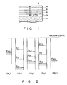
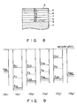
- Fig. 1 shows a sectional structure of an organic EL device according to the first embodiment.
- This EL device can be obtained by sequentially forming films on a glass substrate 1 by, e.g., vacuum evaporation or vacuum sublimation, as will be described later.
- Three organic films are sandwiched between upper first electrodes (M1) 2 and a lower second electrode (M2) 3. More specifically, a first organic film (O1) 4 is formed to be in contact with the first electrode 2, and a second organic film (O2) 5 is formed to be in contact with the second electrode 3.
- a third organic film (O3) 6 serving as a light-emitting layer is sandwiched between the first and second organic films 4 and 5.
- the second electrode 3 in this embodiment is a transparent electrode of, e.g., ITO formed on the glass substrate 1. Light emitted from the EL device is extracted from the substrate 1 side.
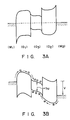
- Fig. 2 is an energy band chart in a state wherein layers which constitute the EL device are isolated from each other.
- materials are selected to satisfy the following inequalities: E C3 > E C1 > E C2 E V1 > E V2 > E V3 where E C1 , E1, and E V1 are the conduction band level, the Fermi level, and the valence band level of the first organic film (O1) 4, E C2 , E2, and E V2 are the conduction band level, the Fermi level, and the valence band level of the second organic film (O2) 5, and E C3 , E3, and E V3 are the conduction band level, the Fermi level, and the valence band level of the third organic film (O3) 6.
- a work function E M1 satisfies the following inequality: E M1 ⁇ E1 More specifically, electrons are easily injected from the first electrode 2 into the first organic film 4.
- a work function E M2 satisfies the following inequality: E M2 > E2 More specifically, holes are easily injected from the second electrode 3 into the second organic film 5.
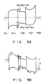
- Fig. 3A is an energy band chart showing the EL device of this embodiment in a thermal equilibrium state.
- the Fermi levels of the components of the device coincide with each other.
- a junction is formed between the first electrode 2 and the first organic film 4 such that electrons are easily injected from the first electrode 2 into the first organic film 4, as shown in Fig. 3A.
- a junction is formed between the second electrode 3 and the second organic film 5 such that holes are easily injected from the second electrode 3 into the second organic film 5.
- the third organic film 6 with a band gap smaller than those of the organic films 4 and 5 is sandwiched between the first and second organic films 4 and 5.
- Fig. 3B is an energy band chart of the device obtained when a given positive biasing voltage V with respect to a voltage applied to the first electrode 2 is applied to the second electrode 3. Electrons are injected from the first electrode 2 into the first organic film 4, and holes are injected from the second electrode 3 into the second organic film 5. These injected electrons and holes are trapped in the third organic film 6 serving as a potential well with respect to both the electrons and holes. The electrons and holes trapped in the third organic film 6 are recombined with each other to perform light emission. Since the band gaps of the first and second organic films 4 and 5 are larger than that of the third organic film 6, light emitted from the third organic film 6 is extracted to the outside without being absorbed in the first and second organic films 4 and 5.
- a device with a structure of a metal electrode 11/a silicon 12/a silicon oxide film 13/an organic film 14/a metal electrode 15 is formed.
- a triangular-wave voltage shown in Fig. 32 is applied to this device, and a displacement current of the device at this time is measured.
- the device is illuminated by a near infra-red ray with a wave length of 800 nm or more. Thereby, the surface of the silicon 12 is immediately inversed and serves as an electrode like to a metal.
- the capacitance of this MOS device is determined by the permittivity and thickness of the silicon oxide film 13. In contrast to this, when the organic film 14 is formed, the following displacement current is observed in accordance with the difference between the Fermi level of the organic film 14 and the work function of the metal electrode 15.
- the junction between the metal electrode 15 and the organic film 14 has a high blocking barrier with respect to both electrons and holes. Therefore, the organic film 14 serves as an insulating member, and hence the capacitance of the device is a series capacitance of the silicon oxide film and the organic film. This capacitance is constant and smaller than that of a normal MOS device.
- the displacement current - voltage characteristics obtained when the triangular-wave voltage shown in Fig. 32 is applied to the device exhibit a constant displacement current value regardless of a voltage, as shown in Fig. 33.
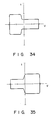
- the junction between the metal electrode 15 and the organic film 14 is formed such that electrons are easily injected from the metal electrode 15 into the organic film 14. Therefore, when the triangular-wave voltage shown in Fig. 32 is applied to the device, and the metal electrode 15 is set to be at a negative potential, electrons are injected from the metal electrode 15 into the organic film 14. The injected electrons are accumulated at the interface between the organic film 14 and the oxide film 13. In this state, the capacitance of the device is determined by the oxide film 13. As shown in Fig. 34, therefore, the displacement current is increased up to the level of a normal MOS device. When the application voltage sets the metal electrode 15 at a positive potential, electrons in the organic film 14 flow out toward the metal electrode 15, and the displacement current is decreased to a small value obtained when the organic film 14 serves as an insulating member.
- the junction between the metal electrode 15 and the organic film 14 is formed such that holes are easily injected from the metal electrode 15 into the organic film 14. Therefore, when the triangular-wave voltage shown in Fig. 32 is applied to the device, and the metal electrode 15 is set at a positive potential, holes are injected from the metal electrode 15 into the organic film 14. The injected holes are accumulated at the interface between the organic film 14 and the oxide film 13. In this state, the capacitance of the device is determined by the oxide film 13. As shown in Fig. 35, the displacement current is increased up to the level of a normal MOS device. When the application voltage sets the metal electrode 15 at a negative potential, holes in the organic film 14 flow out toward the metal electrode 15, and the displacement current is decreased to a small value obtained when the organic film 14 serves as an insulating member.
- the displacement current of the device shown in Fig. 31 is measured.
- the junction state between the metal electrode 15 and the organic film 14 is determined depending on whether the measurement result shown in Fig. 33, 34, or 35 is obtained.
- the organic film 14 has a two-layered structure, a portion in contact with the metal electrode 15 serves as a first organic film 141, and a portion under the first organic film 141 serves as a second organic film 142. Assume that electrons are injected from the metal electrode 15 into the first organic film 141. This has been already examined in the device having an organic film with a single-layer structure. If a displacement current is supplied to the level of the normal MOS device when the metal electrode 15 is at a negative potential, the electrons injected into the first organic film 141 are further injected into the second organic film 142.
- the conduction band level of the second organic film 142 is lower than that of the first organic film 141. If such a MOS device level displacement current is not observed, it is seen that the conduction band level of the second organic film 142 is higher than that of the first organic film 141.
- the relationship between the valence band levels of the two organic films can be examined by a similar displacement current measurement utilizing hole injection.
- the process for manufacturing the device is as follows. First, the second organic film 5 is formed on a glass substrate on which an ITO film is formed by vacuum sublimation (vacuum degree: up to 10 ⁇ 6 torr) to have a thickness of 200 to 1,000 ⁇ . Then, the third and first organic films 6 and 4 are sequentially formed by a similar vacuum sublimation each to have a thickness of 200 to 1000 ⁇ . Finally, an erbium film is formed by vacuum evaporation to have a thickness of 200 to 1,000 ⁇ .
- an EL device which does not have the first and second organic films 4 and 5, but has the third organic film 6 with a single-layer structure as an emitting layer was manufactured. Even if a current of 100 mA was supplied to the EL device at 20 V, a luminance was 500 Cd/m2, and a emission efficiency was about 0.5%. Therefore, it is seen that trapping of carriers performed by sandwiching the light-emitting layer between the first and second organic films contributes to the improvement in emission efficiency.
- Fig. 4 is an energy band chart before junction of the layers of an EL device according to one of the two embodiments.
- Fig. 4 corresponds to Fig. 2.
- the following condition is satisfied between second and third organic films 5 and 6: E V2 ⁇ E V3
- the following condition is satisfied between first and third organic films 4 and 6: E Cl ⁇ E C3
- the other conditions are the same as those in the above embodiment.
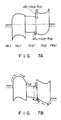
- Figs. 5A and 5B are energy band charts for explaining an operation of an organic EL device of this embodiment.
- Fig. 5A is an energy band chart in a thermal equilibrium state.
- a blocking barrier is formed between the first and third organic films 4 and 6 to block the flow of electrons from the first organic film 4 to the third organic film 6.
- This blocking barrier which blocks the electrons is smaller than a blocking barrier which blocks the flow of holes from the third organic film 6 to the first organic film 4.
- FIG. 5B A state wherein a forward biasing voltage is applied to the EL device of this embodiment is shown in Fig. 5B. Electrons injected from a first electrode 2 into the first organic film 4 are accumulated at the blocking barrier junction between the first and third organic films 4 and 6. The holes injected from a second electrode 3 into the second organic film 5 are supplied to the third organic film 6, and are accumulated at the blocking barrier junction between the third and first organic films 6 and 4. Thus, the carriers accumulated at the junction between the first and third organic films 4 and 6 form an electric double layer. The thickness of the electric double layer is equal to the intermolecule distance (up to 10 ⁇ ) of the organic dye.
- a high-intensity electric field of about 107 V/cm or more is formed in the electric double layer.
- the electrons in the first organic film 4 are tunnel-injected into the third organic film 6 by this strong electric field to perform radiative recombination in the third organic film 6.
- Fig. 6 is an energy band chart before junction of layers of another device.
- the following condition is set between first and third organic films 4 and 6: E C1 ⁇ E C3
- the following condition is set between the second and third organic films 5 and 6: E V2 ⁇ E V3
- the other conditions are the same as those of the device shown in Fig. 2.
- Figs. 7A and 7B are energy band charts for explaining an operation of an organic EL device of this embodiment.
- Fig. 7A is an energy band chart in a thermal equilibrium state.
- a blocking barrier is formed between the second and third organic films 5 and 6 to block the flow of holes from the second organic film 5 to the third organic film 6.
- a state wherein a forward biasing voltage is applied to the EL device of this embodiment is shown in Fig. 7B.
- the electrons injected from a first electrode 2 into the first organic film 4 are supplied to the third organic film 6, and are accumulated at the blocking barrier junction between the third and second organic films 6 and 5.
- the holes injected from a second electrode 3 into the second organic film 5 are accumulated at the blocking barrier junction between the second and third organic films 5 and 6.
- the carriers accumulated at the junction between the second and third organic films 5 and 6 form an electric double layer. If the biasing voltage exceeds a predetermined value, holes in the second organic film 5 are tunnel-injected into the third organic film 6 to perform radiative recombination in the third organic film 6.
- Fig. 8 is a sectional view showing the structure of an organic EL device of such an embodiment. As is apparent from a comparison with Fig. 1, in this embodiment, an emitting layer region sandwiched between first and second organic films 4 and 5 is a multi-layered body of third and fourth organic films 6 and 7.
- Fig. 9 is an energy band chart before junction of layers of the EL device of this embodiment. As shown in Fig. 9, in this embodiment, materials are combined to satisfy the following conditions: E1 > E3 > E4 > E2 E C3 - E V3 ⁇ E C1 - E V1 E C4 - E V4 ⁇ E C2 - E V2 E C1 ⁇ E C3 > E C4 E V2 ⁇ E V4 ⁇ E V3
- Fig. 10A is an energy band chart of the EL device of this embodiment in a thermal equilibrium state.
- the third and fourth organic films 6 and 7 each having a small band gap are sandwiched between the first and second organic films 4 and 5 each having a large band gap.
- a conduction band the interface between the first and third organic films 4 and 6 is smooth, and a blocking barrier is formed between the third and fourth organic films 6 and 7.
- This barrier to block electrons is smaller than that between the fourth and second organic films 7 and 5.
- a valence band the interface between the second and fourth organic films 5 and 7 is smooth, and a blocking barrier is formed between the third and fourth organic films 6 and 7.
- Fig. 10B is an energy band chart obtained when a biasing voltage is applied to the EL device of this embodiment to set a second electrode 3 at a positive potential with respect to the first electrode. Electrons are injected from a first electrode 2 into the first organic film 4. The injected electrons are transferred to the third organic film 6, and are accumulated at the blocking barrier junction between the third and fourth organic films 6 and 7. Holes are injected from the second electrode 3 into the second organic film 5. The injected holes are transferred to the fourth organic film 7, and are accumulated at the blocking barrier junction between the third and fourth organic films 6 and 7. Thus, in this embodiment, an electric double layer is formed in the junction between the third and fourth organic films 6 and 7.
- biasing voltage exceeds a predetermined value, electrons are tunnel-injected from the third organic film 6 into the fourth organic film 7 to perform radiative recombination in the fourth organic film 7. At the same time, or at a different threshold voltage, holes are tunnel-injected from the fourth organic film 7 into the third organic film 6 to perform radiative recombination in the third organic film 6.
- the threshold value of the hole injection from the fourth organic film 7 into the third organic film 6 is equal to that of the electron injection from the third organic film 6 into the fourth organic film 7, light emission in the third organic film 6 is mixed with light emission in the fourth organic film 7. If these threshold values are different from each other, light emission in one organic film has priority over that in the other organic film. For example, light emission in the third organic film 6 occurs at the first threshold value. A biasing voltage is further increased, and light emission in the fourth organic film 7 overlaps the light emission in the third organic film 6 at the second threshold value. This priority order can be reversed depending on the film materials. Regardless of the priority, in this case, one-pixel multi-color display capable of emission color control by a biasing voltage can be realized.
- the third and fourth organic films serving as emitting layers are sandwiched between the first and second organic films each having a large band gap. Therefore, high-efficiency light emission can be achieved by a carrier trapping effect.
- First Electrode 2 erbium film
- Second Electrode 3 ITO film
- First Organic Film 4 tetranitrobifluorenonyl
- Forth Organic Film 7 bicoronenyl
- the process for manufacturing the device is basically the same as that described above.
- a biasing voltage was applied to the obtained device, a current of about 10 mA flowed at an application voltage of 5 V, and light emission with a luminance of about 2,000 Cd/m2 was recognized.
- a emission efficiency was about 20%.
- the multi-color EL device according to the present invention basically has a multi-layered structure consisting of the first and second organic films in which a blocking barrier junction is formed to block electrons or holes, and the first and second electrodes which sandwich this multi-layered structure.
- the first electrode for electron injection is formed on the first organic film side
- the second electrode for hole injection is formed on the second organic film side.
- the first multi-color organic EL device utilizes the following phenomenon. That is, when a positive biasing voltage with respect to the second electrode is applied between the first and second electrodes, electrons injected from the first electrode into the first organic film and holes injected from the second electrode into the second organic film are accumulated at the interface of the blocking barrier junction. Of the accumulated electrons and holes, the electrons are tunnel-injected into the second organic film to perform radiative recombination in the second organic film, and the holes are tunnel-injected into the first organic film to perform radiative recombination in the first organic film.
- E M1 and E M2 are the work functions of the first and second electrodes, respectively, E C1 , E1, and E V1 are the conduction band level, the Fermi level, and the valence band level of the first organic film, respectively, and E C2 , E2, and E V2 are the conduction band level, the Fermi level, and the valence band level of the second organic film, respectively.
- materials are selected to satisfy the following condition (5) or (6) in addition to the above conditions (1) to (4): EC1 - EC1 ⁇ E V1 - E V2 (5) EC1 - EC1 > E V1 - E V2 (6)
- the second multi-color organic EL device has a structure obtained by additionally inserting the third organic film between the second organic film and the second electrode in addition to the above-mentioned basic structure.
- a positive biasing voltage with respect to the second electrode is applied between the first and second electrodes, electrons injected from the first electrode into the first organic film and holes injected from the second electrode into the second organic film through the third organic film are accumulated at the interface of the blocking barrier junction.
- the electrons are tunnel-injected into the second organic film at the first threshold voltage to perform radiative recombination in the second organic film, and are further injected into the third organic film at the second threshold voltage to perform radiative recombination in the third organic film.
- materials are selected to satisfy the following conditions (7) to (10) in addition to the relationship of the electrical characteristics in the materials of the first multi-color organic EL device: E C1 - E C2 ⁇ E V1 - E V2 (7) E C2 ⁇ E C3 (8) E V2 ⁇ E V3 (9) E M2 ⁇ E3 (10) where E C3 , E3, and E V3 are the conduction band level, the Fermi level, and the valence band level of the third organic film.
- the third multi-color organic EL device has a structure obtained by additionally inserting the third organic film between the first electrode and the first organic film in the above-mentioned basic structure.
- a positive biasing voltage with respect to the second electrode is applied between the first and second electrodes, electrons injected from the first electrode into the first organic film through the third organic film, and holes injected from the second electrode into the second organic film are accumulated at the interface of the blocking barrier junction.
- the holes are tunnel-injected into the first organic film at the first threshold voltage to perform radiative recombination in the first organic film, and are further injected into the third organic film at the second threshold voltage to perform radiative recombination in the third organic film.
- materials are selected to satisfy the following conditions (11) to (13) in addition to the relationship of the electrical characteristics of the materials in the first multi-color organic EL device: E C1 - E C2 > E V1 - E V2 (11) E C3 ⁇ E C1 (12) E V3 ⁇ E V1 (13) E M1 ⁇ E3 (14) where E C3 , E3, and E V3 are the conduction band level, the Fermi level, and the valence band level of the third organic film.
- blocking barriers to block electrons and holes are formed on the junction interface between the first and second organic films (conditional inequalities (3) and (4)).
- a biasing voltage to set the second electrode at a positive potential is applied, electrons are injected from the first electrode into the first organic film (conditional inequality (1)), and holes are injected from the second electrode into the second organic film (conditional inequality (2)).
- conditional inequality (1) a biasing voltage to set the second electrode at a positive potential
- the first multi-color organic EL device therefore, when a biasing voltage exceeds a predetermined threshold value, electrons in the first organic film are injected into the second organic film to perform radiative recombination in the second organic film. If the biasing voltage exceeds a predetermined threshold value, holes in the second organic film are tunnel-injected into the first organic film to perform radiative recombination in the first organic film. Thus, light emission with a wavelength determined by the first organic film and light emission with a wavelength determined by the second organic film can be obtained. When the conditional inequality (5) is satisfied, tunnel injection of electrons from the first organic film into the second organic film has priority over that of holes.
- a blocking barrier which blocks electrons is set to be lower than that which blocks holes (conditional inequalities (7) and (8)).
- materials are selected so that holes injected from the second electrode into the third organic film are supplied to the second organic film with little interference (conditional inequalities (9) and (10)). Therefore, of carriers accumulated at the blocking barrier junction between the first and second organic films to form, an electric double layer upon application of a biasing voltage, electrons are tunnel-injected into the second organic film to perform radiative recombination in the second organic film.
- the multi-color EL device capable of emission color control by a biasing voltage can be obtained.
- a blocking barrier which blocks holes is set to be lower than that which blocks electrons (conditional inequalities (11) and (12)).
- materials are selected so that electrons injected from the first electrode into the third organic film are supplied to the second organic film with little interference. Therefore, of the carriers accumulated at the blocking barrier junction between the first and second organic films to form an electric double layer upon application of a biasing voltage, holes are tunnel-injected into the first organic film to perform radiative recombination in the first organic film.
- the biasing voltage is further increased, a large number of holes are supplied to the third organic film to perform radiative recombination in the third organic film. Therefore, the multi-color EL device capable of emission color control by a biasing voltage can be obtained.
- Fig. 11 shows a sectional device structure of the first multi-color organic EL device of the embodiment.
- This device includes a first electrode (M1) 2, a first organic film (O1) 4, a second organic film (O2) 5, and a second electrode (M2) 3, in the order named from the upper side.
- the second electrode 3 is a transparent electrode of, e.g., ITO formed on a glass substrate 1 in this embodiment. Light is extracted from the glass substrate 1 side.
- the films are sequentially stacked on the substrate by, e.g., vacuum evaporation or vacuum sublimation, in the same manner as in the above embodiments.
- Fig. 12 is an energy band chart in a state wherein the layers which constitute the multi-color EL device are isolated from each other.
- materials are selected to satisfy the following inequalities: E C1 >E C2 E V1 > E V2
- E C1 , E1, and E V1 are the conduction band level, the Fermi level, and the valence band level of the first organic film 4
- E C2 , E2, and E V2 are the conduction band level, the Fermi level, and the valence band level of the second organic film 5.
- the first electrode 2 has a work function E M1 which satisfies the following inequality: E M1 ⁇ E1 Electrons are easily injected from the first electrode 2 into the first organic film 4.
- the second electrode 3 has a work function E M2 which satisfies the following inequality: E M2 >E2 Holes are easily injected from the second electrode 2 into the second organic film 5.
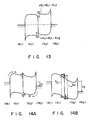
- Fig. 14A is an energy band chart of the device obtained when a given positive biasing voltage V1 with respect to a voltage applied to the first electrode 2 is applied to the second electrode 3. Electrons are injected from the first electrode 2 into the first organic film 4, and holes are injected from the second electrode 3 into the second organic film 5. These injected electrons and holes are accumulated at the blocking barrier junction interface between the first and second organic films 4 and 5 to form an electric double layer. As shown in Fig.
- the carriers which form the electric double layer are tunnel-injected in an adjacent layer through the blocking barrier junction.
- the holes injected from the second organic film 5 into the first organic film 4 are recombined with the electrons which are major carriers in the first organic film 4, thereby obtaining light emission with a first wavelength of ⁇ 1.
- the electrons injected from the first organic film 4 into the second organic film 5 are recombined with the holes which are major carriers in the second organic film 5, thereby obtaining light emission with a second wavelength of ⁇ 2.
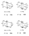
- Figs. 15A and 15B are energy band charts for explaining an operation of the multi-color EL device in which materials are selected to satisfy the following inequality: E C1 - E C2 ⁇ E V1 - E V2
- E C1 - E C2 ⁇ E V1 - E V2 electrons and holes are respectively injected into the first and second organic films 4 and 5 by the biasing voltage V to form the electric double layer.
- the biasing voltage V exceeds a first threshold voltage Vth1
- electrons are tunnel-injected from the first organic film 4 into the second organic film 5 to perform radiative recombination in the second organic film, thus emitting light with the wavelength of ⁇ 2, as shown in Fig. 14A.
- Figs. 16A and 16B are energy band charts for explaining an operation of the multi-color EL device in which materials are selected to satisfy the following inequality: E C1 - E C2 > E V1 - E V2
- E C1 - E C2 > E V1 - E V2 In this case, in contrast to Figs. 15A and 15B, light emission in the first organic film 4 (wavelength ⁇ 1) occurs at the first threshold voltage Vth1, and light emission (wavelength ⁇ 2) in the second organic film 5 overlaps the above light emission at the second threshold voltage Vth2.
- the first and second threshold voltages Vth1 and Vth2 and the wavelengths ⁇ 1 and ⁇ 2 in Figs. 16A and 16B are normally not equal to those in Figs. 15A and 15B.
- First Electrode 2 erbium film
- Second Electrode 3 ITO film
- Second Organic Film 5 bipyrenyl
- the process for manufacturing the device is as follows. First, the second organic film having a thickness of 1,000 ⁇ is formed on a glass substrate on which an ITO film is formed by vacuum sublimation (vacuum degree ⁇ 10 ⁇ 6 Torr). Similarly, the first organic film is formed on the second organic film to have a thickness of 1,000 ⁇ by vacuum sublimation. Finally, the erbium film having a thickness of 1,000 ⁇ is formed by vacuum evaporation.
- the process for manufacturing the device and the thickness of each layer are the same as those in the above multi-color EL device.
- the multi-color EL device using a two-layered organic film structure has been described above.
- three organic films can be combined to form a multi-color EL device on the basis of the two-layered structure. Such embodiments will be described below.
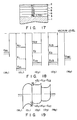
- Fig. 17 is a sectional view of a multi-color organic EL device of such an embodiment. Unlike in Fig. 11, a third organic film 6 is sandwiched between a second organic film 5 and a second electrode 3 in this embodiment.
- Fig. 18 shows the electrical characteristics, e.g., a work function of each layer in the EL device shown in Fig. 17.
- a relationship of the material characteristics between a first electrode 2, a first organic film 4, the second organic film 5, and the second electrode 3 is basically the same as that of the multi-color EL device shown in Fig. 11.
- the energy levels of the first and second organic films 4 and 5 are set to have the following relationship: E C1 - E C2 ⁇ E V1 - E V2
- E C3 is the conduction band level
- E3 is the Fermi level
- E V3 is the valence band level.
- Blocking barriers are formed between the first and second organic films 4 and 5 to block electrons and holes, respectively, as in the above embodiments.
- a blocking barrier ⁇ E C which blocks electrons on the conduction band side is formed to be smaller than a blocking barrier ⁇ E V which blocks holes on the valence band side.
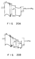
- the thickness of the second organic film 5 is smaller than the mean free path of the carriers, and a blocking barrier which blocks the flow of electrons from the second organic film 5 to the third organic film 6 is not formed. Holes are easily injected from the second electrode 3 into the third organic film 6, and the holes injected into the third organic film 6 are supplied to the second organic film 5 with little interference.
- a large number of electrons injected from the first organic film 4 into the second organic film 5 are further injected into the third organic film 6 without being recombined, as shown in Fig. 20B.
- the injected electrons are recombined with the holes in the third organic film 6 to emit light. More specifically, light with a short wavelength is emitted from the second organic film 5 with a large band gap under the low-bias condition. Under the high-bias condition, light with a long wavelength emitted from the third organic film 6 with a small band gap is mixed with the light from the film 5.
- the second organic film 5 serves as a blue emitting agent
- the third organic film 6 serves as a yellow emitting agent
- blue light is emitted at a low biasing voltage
- white light is emitted at a high biasing voltage.
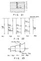
- Fig. 21 is a multi-color EL device according to another embodiment using a three-layered structure of organic films.
- a third organic film 6 is formed between a first electrode 2 and a first organic film 4.
- Fig. 22 shows energy levels before junction of layers of the EL device of this embodiment.
- the energy levels of the first and second organic films 4 and 5 are set to have the following relationship opposite to that in Fig. 17: E C1 - E C2 > E V1 - E V2
- the levels of the third organic film 6 are set as follows on the basis of the relationship between the first organic film 4 and the first electrode 2: E C3 - E C1 E V3 ⁇ E V2 E3 > E M1 where E C3 is the conduction band level, E3 is the Fermi level, and E V3 is the valence band level.
- Fig. 23 is, therefore, an energy band chart of the EL device in which these layers are connected to each other in a thermal equilibrium state.
- Blocking barriers are formed between the first and second organic films 4 and 5 to block electrons and holes, respectively, as in the above embodiments.
- a blocking barrier ⁇ E C which blocks electrons on the conduction band is formed to be higher than a blocking barrier ⁇ E V which blocks holes on the valence band.
- the thickness of the second organic film 5 is smaller than the mean free path of the carriers, and a blocking barrier which blocks the flow of holes from the second organic film 5 to the third organic film 6 is not formed. Electrons are easily injected from the first electrode 2 into the third organic film 6, and the electrons injected into the third organic film 6 are supplied to the second organic film 5 without interference.
- Figs. 24A and 24B are energy band charts showing an operation of multi-color light emission in the multi-color EL device of this embodiment.
- a biasing voltage Upon application of a biasing voltage, an electric double layer is formed in the blocking barrier junction between the first and second organic films 4 and 5, as in the above embodiments.
- Vth1 a first threshold value
- holes in the second organic film 5 are tunnel-injected into the first organic film 4 to perform radiative recombination in the first organic film 4, as shown in Fig. 24A.
- a threshold value Vth2 When the biasing voltage is further increased to exceed a threshold value Vth2, a large number of holes are injected into the third organic film 6 to perform radiative recombination in the third organic film 6, as shown in Fig. 24B.
- multi-color light emission to cause a biasing voltage to control an emission color can be achieved.
- the device shown in Fig. 17 consisted of the following materials.
- First Electrode 2 erbium film
- Second Electrode 3 ITO film
- First Organic Film 4 bis(dicyano-9-fluorenonyl)ethane
- Second Organic Film 5 bipyrenyl
- Third Organic Film 6 bicoronenyl
- the device shown in Fig. 21 consisted of the following materials.
- First Electrode 2 erbium film
- Second Electrode 3 ITO film
- the process for manufacturing the device is the same as in the above embodiments.
- a large number of display pixels are arranged in a matrix form, and are time-divisionally driven.
- a method for driving the pixels is classified into simple and active matrix methods. Regardless of the method used, a drive voltage pulse is applied to one pixel, and a voltage application time is extremely short. For this reason, in order to obtain a high-quality image, each pixel must have a memory function to some extent.
- the capacitance of the liquid crystal itself, or a capacitor arranged in parallel with the liquid crystal has the memory function.
- the organic EL device When the organic EL device is applied to such a matrix-driven flat panel display, the device must have a memory function. So far, however, such a memory function of the organic EL device has not been reported.
- the light-emission characteristics of the device can have a memory function.
- electron-injection electrodes are formed on the upper and lower surfaces of the light-emitting organic film, only electrons are injected into the organic film upon application of a biasing voltage.
- the carrier mobility of the organic material used for the EL device is as small as 10 ⁇ 3 cm2/V ⁇ sec.
- this current serves as a space-charge limited current (which is in proportion to the square of a voltage) limited by the internal electric field.
- one electrode is of an electron injection type, and the other electrode is of a hole injection type. Therefore, electrons and holes are simultaneously injected and accumulated in the organic films upon application of a biasing voltage.
- An electric-charge state of each organic film is neutralized when carrier recombination occurs, thereby increasing the carrier mobility. More specifically, so-called conductivity modulation occurs in the organic films, and a resistance is decreased to supply a large current.
- hysteresis characteristics appear in the electrical characteristics of the organic EL device according to the present invention.
- negative resistance characteristics appear.
- a memory function is generated in the light-emission characteristics. In addition, this memory function appears as an afterimage phenomenon.
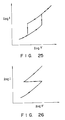
- Fig. 25 shows voltage - current characteristics obtained when the EL device of the embodiment shown in Fig. 11 is driven by a constant voltage.
- Fig. 26 shows voltage - current characteristics obtained when the device of this embodiment is driven by a constant current.
- a current represented on the axis of ordinate in each of Figs. 25 and 26 corresponds to light-emission luminance.
- a current direction with which the first electrode 2 side is set to have a negative polarity is the forward direction.
- a forward current flows by tunnel injection achieved by forming an electric double layer.
- a current does not flow upon application of a reverse voltage because carriers are not injected from the upper and lower electrodes.
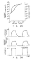
- a triangular-wave AC biasing voltage shown in Fig. 32 is applied to the EL device, and a displacement current is measured.
- a measurement region corresponds to a very small current region near the origin of the voltage - current characteristics. This region is surrounded by a broken line in Fig. 27.
- Fig. 28 shows the obtained potential current characteristics.
- a reverse bias region i.e., on the right side with respect to a point A in Fig. 28, carriers are not injected into the organic films, as described above, and hence electric charges are accumulated between the upper and lower electrodes.
- the interelectrode layers serve as a capacitor which sandwiches two organic films serving as insulating members. Therefore, the capacitance is small. As a result, the displacement current is also small.
- First Electrode 2 ytterbium film
- Second Electrode 3 ITO film
- First Organic Film 4 bi(9-malononitrilefluorenyl)
- Second Organic Film 5 bipyrenyl (emitting layer)
- the process for manufacturing the device is the same as in the above embodiments.
- a light-emitting layer is constituted by an organic film formed by dispersing 10 mol% or less of a second organic dye having a light-absorption end at a long wavelength side with respect to a first organic dye as a major constituent.
- the characteristics required for the first organic dye are, e.g., that carriers injected from the electrode are efficiently recombined, that dye molecules are efficiently excited by the carrier recombination, and that the occurrence of non-radiative recombination process from the excited state is minimized.
- the characteristics required for the second organic dye are that excitation energy can be efficiently received from the first organic dye in the excited state to emit light with a specific wavelength.
- the excited state of the first organic dye is classified into two states, i.e., a singlet and doublet states. It is known that, of these two states, fluoroscence from the excited singlet contributes to light emission in the organic EL device. Therefore, a component which easily allows a singlet - singlet excitation energy transfer is preferably selected as the second organic dye. Overlapping of a fluoroscent spectrum from the first organic dye and a light-absorption spectrum from the second organic dye is a reference for selection of the second organic dye. In general, the wavelength of the light-absorption end of the second organic dye need only be longer than that of the light-absorption spectrum of the first organic dye.
- organic EL device In the organic EL device, at a room temperature, contribution of phosphorescence emitted from the dye in another excited state, i.e., a triplet state, is not recognized. This is because, a large number of organic dyes do not emit phosphorescence at a normal temperature although they emit phosphorescence at low temperatures. Therefore, it is effective to select a component which receives energy from the first organic dye in the excited triplet state to be excited, and emits phosphorescence or fluoroscence at a normal temperature, as the second organic dye.
- the second organic dye dispersed in the first organic dye is not limited to one type, but two or more types of dyes may be dispersed.
- an organic dye which receives energy from the first organic dye in the excited singlet state and an organic dye which receives energy from the excited triplet state are dispersed in the first organic dye, light can be emitted more efficiently.
- a plurality of dye are dispersed in the first organic dye as the second organic dye, light-emission characteristics with many wavelengths can be obtained. More specifically, when the second organic dye is selected, light-emission intensities of red, green, and blue can be controlled, thereby efficiently obtaining white light emission.
- the above description will be summarized hereinafter. It is effective to disperse the second organic dye in the first organic dye in order to solve the following problems which occur when an emitting layer is constituted by only one dye.
- the first problem is that it is difficult to generate phosphorescence from the excited triplet state during a light-emission process in a normal organic dye.
- the second problem is that if non-emitting sites are present at a rate of at least one per 103 to 105 molecules during the transfer process of the excitation energy, light emission is not observed.
- the third problem is that when molecules in the excited state are polymerized and stabilized, the light-emission wavelength is shifted to the long wavelength side.
- the first problem can be solved by using an organic dye which can emit phosphorescence at a normal temperature as the second organic dye. Therefore, energy from the first organic dye in the excited triplet state can be efficiently utilized.
- organic dyes include, e.g., a dye having a carbonyl group, a dye in which hydrogen is substituted by heavy hydrogen, and a dye containing a heavy element such as a halogen. These substitution groups function to accelerate emission of phosphorescence. However, it is not preferable to add such an organic dye at a high concentration because it causes degeneration of the excited singlet.
- the second problem can be solved by dispersing the second organic dye in the first organic dye at a concentration higher than the non-emitting sites. Therefore, the transfer of energy of the first organic dye in an excited state, in particular, an excited singlet state to the non-emitting site can be prevented, and the energy transfer to the second organic dye occurs. As a result, high-efficiency light emission can be achieved.
- the third problem can be solved by transferring energy of the first organic dye to the second organic dye before the first organic dye in the excited state is polymerized and stabilized.
- the ratio of the second organic dye with respect to the first organic dye must, therefore, be suppressed at a proper value to keep the second organic dye in an isolated state.
- the ratio of the second organic dye with respect to the first organic dye exceeds 10 mol%, the probability of dimerization or polymerization of the excited second organic dye is increased.
- the wavelength of the emitted light is shifted toward the long-wavelength side as compared with light emission from the isolated second organic dye.
- the ratio of the second organic dye to be dispersed in the first organic dye is preferably suppressed to be 10 mol% or less.
- a method for forming a light-emitting layer by dispersing the second dye in the first organic dye is classified into the following two methods.
- the sublimated and refined first organic dye material is selected for the first organic dye, and the second organic dye material is mixed with the first organic dye material at a ratio of 0.01 to 1 mol%.
- This mixed material is heated and fused under stirring in a quartz container while an argon gas is added. After the crystals are perfectly mixed with each other, the resultant mixture is relatively quickly cooled and solidified.
- a light-emitting layer is formed by vacuum sublimation.
- an EL device having a light-emitting layer obtained by dispersing the second organic dye in the first organic dye was manufactured and its characteristics were measured.
- the structure of the EL device is the same as in Fig. 1, and materials therefor are selected as follows.
- First Electrode 2 erbium film
- Second Electrode 3 ITO film
- First Organic Dye bipyrenyl
- Second Organic Dye bicoronenyl
- the EL device having the light-emitting layer containing such two types of organic dyes a current of about 4 mA flowed at a DC voltage of 30 V, and light emission with a maximum luminance of 5,000 cd/m2 could be obtained.
- the light-emission spectrum is slightly shifted toward the long-wavelength side as compared with a case wherein only the first organic dye is used.
- the addition amount of the second organic dye preferably falls within the range of 0.1 to 1 mol%.
- the second organic dye contained in the light-emitting layer e.g., (a) a condensed polycyclic aromatic dye consisting of only elements C and H, (b) a condensed polycyclic aromatic dye containing in its skeleton a hetero atom such as O, N, or S besides elements C and H, or (c) a fluoroscent dye developed for a dye laser can be used.
- a condensed polycyclic aromatic dye consisting of only elements C and H e.g., (a) a condensed polycyclic aromatic dye consisting of only elements C and H, (b) a condensed polycyclic aromatic dye containing in its skeleton a hetero atom such as O, N, or S besides elements C and H, or (c) a fluoroscent dye developed for a dye laser can be used.
- the organic dye material used in the present invention will be described hereinafter in detail.
- the following conditions are required for an organic EL device. That is, (1) high emission efficiency, (2) a high luminance, (3) blue light emission which cannot be obtained in a conventional LED, (4) driving at a low voltage, and the like.
- the conditions (1) and (2) it is important to optimally select the electronic properties of electron donor-type and electron-acceptor type dyes.
- As for the condition (3) it is important to select a dye with a large band gap as a dye used for a light-emitting layer.
- the absorption position of the dye i.e., a band gap
- the absorption position of the dye i.e., a band gap
- the condition (4) since a high-intensity electric field must be applied to the organic film, it is important to decrease the thickness of the organic film. However, it is not easy to decrease the thickness of the organic film, and to obtain high reliability of the device at the same time. This is because of the following reason.
- the organic EL device is obtained by sequentially stacking organic films on a transparent electrode formed on a transparent substrate, and depositing a metal on the uppermost layer.
- the organic film normally has a thickness of 100 to 10,000 ⁇ .
- Vacuum evaporation of the upper electrode is performed under the conditions of a vacuum degree of 10 ⁇ 5 to 10 ⁇ 6 Torr, and a temperature of 200 to 300°C.
- the organic film which has been formed is affected by heat radiated from an evaporation source or heat transmitted by a flying metal atomic beam.
- the worst effect is as follows.
- the dye has a small molecular weight, its evaporation pressure is high. Therefore, the dye is sublimated again due to the above-mentioned heat to cause defects. In addition, heat fuses the organic film to cause defects, thus undesirably disabling application of a predetermined voltage.
- a light-emitting dye such as anthracene, which has a small molecular weight and emits blue light, is used in practice, a production yield of the device is extremely low.
- a polymer obtained by linking two or more dyes each having a band gap of 3 eV or more via a non-conjugated link is preferivelyably used as an organic dye used for an organic EL device.
- the molecular weight of each organic dye used for a light-emitting layer is preferably 400 or more.
- Various molecules can be used as such a dye molecule having a large molecular weight.
- a molecular structure must be taken into consideration.
- a derivative of a condensed polycyclic aromatic molecule having an increased ⁇ electronic conjugated system can be exemplified as a dye molecule with a large molecular weight.
- these dyes are of an electron donor type. Therefore, these dyes are used for hole transport layers.
- an aromatic skeleton is derived to have a quinoid structure, or a netro-, cyano, or halogen-group is introduced to impart an electron acceptor property.
- a polyphiline metal complex and a phthalocyanine metal complex are known as dye molecules with a large molecular weight.
- a polymer obtained by linking two or more organic dyes each having a band gap of 2.6 eV or more via a non-conjugated link may be used.
- an organic dye with a band gap of 2.6 eV or more serving as a monomer may have a molecular weight of 100 to 400.
- a non-conjugated link for linking these organic dyes includes a carbon - carbon link, a hydrocarbon residue, an ester link, a carbonyl residue, an amide link, and an ether link. These organic dyes may be linked to a straight chain polymer in a pendant-like manner. In this case, the non-conjugated link is a repeating unit which constitutes a straight chain.
- Examples of the light-emitting organic dyes each consisting of a polymer obtained by combining two or more organic dyes with a band gap of 2.6 eV or more via a non-conjugated link are shown in tables 1 to 6.
- Tables 3 and 4 respectively show a donor and an acceptor each serving as a monomer which constitutes a light-emitting organic dye.
- Table 5 shows examples of combinations of, e.g., an ester link, a carbonyl residue, an amide link, and an ether link as non-conjugated links.
- reference symbol R denotes a donor or an acceptor.
- Table 6 shows examples of light-emitting organic dyes obtained by linking the donor or acceptor R with a straight chain polymer serving as a monomer in a pendant-like manner.
- an erbium (Er) film and a ytterbium (Yb) film are used as the first electrode which injects electrons into the organic films.
- the following properties are required for the first electrode. That is, easy injection of electrons into the organic film, i.e., a small work function, easy vacuum evaporation, high chemical stability, and the like. From such viewpoints, other rare earth elements such as neodymium (Nd) and gadolinium (Gd) can be used as the first electrode.
Landscapes
- Physics & Mathematics (AREA)
- Optics & Photonics (AREA)
- Chemical & Material Sciences (AREA)
- Spectroscopy & Molecular Physics (AREA)
- Engineering & Computer Science (AREA)
- Materials Engineering (AREA)
- Organic Chemistry (AREA)
- Electroluminescent Light Sources (AREA)
Applications Claiming Priority (8)
| Application Number | Priority Date | Filing Date | Title |
|---|---|---|---|
| JP83568/89 | 1989-03-31 | ||
| JP1083568A JPH02261889A (ja) | 1989-03-31 | 1989-03-31 | 有機電界発光素子 |
| JP254960/89 | 1989-09-29 | ||
| JP1254960A JPH03115486A (ja) | 1989-09-29 | 1989-09-29 | 有機電界発光素子 |
| JP25101/90 | 1990-02-06 | ||
| JP2025100A JPH03230583A (ja) | 1990-02-06 | 1990-02-06 | 有機膜発光素子 |
| JP2510190A JP2991450B2 (ja) | 1990-02-06 | 1990-02-06 | 有機膜発光素子 |
| JP25100/90 | 1990-02-06 |
Publications (3)
| Publication Number | Publication Date |
|---|---|
| EP0390551A2 true EP0390551A2 (fr) | 1990-10-03 |
| EP0390551A3 EP0390551A3 (fr) | 1991-07-10 |
| EP0390551B1 EP0390551B1 (fr) | 1996-07-10 |
Family
ID=27458250
Family Applications (1)
| Application Number | Title | Priority Date | Filing Date |
|---|---|---|---|
| EP90303351A Expired - Lifetime EP0390551B1 (fr) | 1989-03-31 | 1990-03-29 | Dispositif organique électroluminescent |
Country Status (3)
| Country | Link |
|---|---|
| US (1) | US5294810A (fr) |
| EP (1) | EP0390551B1 (fr) |
| DE (1) | DE69027697T2 (fr) |
Cited By (31)
| Publication number | Priority date | Publication date | Assignee | Title |
|---|---|---|---|---|
| EP0498979A1 (fr) * | 1991-02-12 | 1992-08-19 | Kabushiki Kaisha Toshiba | Dispositif électroluminescent organique |
| EP0553950A2 (fr) | 1992-01-07 | 1993-08-04 | Kabushiki Kaisha Toshiba | Dispositif électro-luminescent organique |
| WO1994003030A1 (fr) * | 1992-07-27 | 1994-02-03 | Cambridge Display Technology Limited | Fabrication de dispositifs electroluminescents |
| WO1994003031A1 (fr) * | 1992-07-27 | 1994-02-03 | Cambridge Display Technology Limited | Dispositifs electroluminescents |
| US5366811A (en) * | 1990-09-20 | 1994-11-22 | Idemitsu Kosan Co., Ltd. | Organic electroluminescence device |
| US5653914A (en) * | 1992-12-18 | 1997-08-05 | Cambridge Display Technology Limited | Electroluminescent device comprising a chromophoric polymeric composition |
| EP0812125A3 (fr) * | 1996-06-06 | 1998-06-10 | Motorola, Inc. | Dispositif organique électroluminescent avec émission de la couche transportant des trous de charge |
| EP0880304A3 (fr) * | 1997-05-19 | 1999-06-16 | Canon Kabushiki Kaisha | Dispositif électroluminescent |
| US5922481A (en) * | 1995-01-13 | 1999-07-13 | Basf Aktiengesellschaft | Electroluminescent arrangement |
| WO2000041443A1 (fr) | 1998-12-28 | 2000-07-13 | Idemitsu Kosan Co., Ltd. | Dispositif electroluminescent organique |
| EP1018168A4 (fr) * | 1997-07-11 | 2000-10-18 | Fed Corp | Dispositif electroluminescent organique a haute luminosite et a haut rendement |
| US6384528B1 (en) | 1997-11-21 | 2002-05-07 | Cambridge Display Technology Limited | Electroluminescent device |
| US6489638B2 (en) | 2000-06-23 | 2002-12-03 | Semiconductor Energy Laboratory Co., Ltd. | Light emitting device |
| US6541790B1 (en) | 1996-05-03 | 2003-04-01 | Cambridge Display Technology Limited | Organic light-emitting device and method of fabricating the same |
| US6677621B2 (en) | 2000-05-22 | 2004-01-13 | Semiconductor Energy Laboratory Co., Ltd. | Light emitting device and electrical appliance |
| EP1406127A3 (fr) * | 2002-09-30 | 2005-02-02 | Samsung Electronics Co., Ltd. | Organophotorécepteur comprenant un composé contenant un groupe de toluidine |
| WO2005082851A3 (fr) * | 2004-02-20 | 2005-10-20 | Du Pont | Composes de transport de charge et dispositifs electroniques fabriques avec de tels composes |
| US7227027B2 (en) * | 2003-09-05 | 2007-06-05 | Tsinghua University | Carbazole derivative and its use in electroluminescent devices |
| EP1482573A3 (fr) * | 2003-05-29 | 2007-07-25 | Sony Corporation | Dispositif électroluminescent organique |
| US7372199B2 (en) | 2000-08-28 | 2008-05-13 | Semiconductor Energy Laboratory Co., Ltd. | Light emitting device and image playback device having triplet and singlet compounds in electroluminescent layer |
| US7399991B2 (en) | 2001-02-22 | 2008-07-15 | Semiconductor Energy Laboratory Co., Ltd. | Organic light emitting device and display device using the same |
| US7400087B2 (en) | 2000-06-05 | 2008-07-15 | Semiconductor Energy Laboratory Co., Ltd. | Light-emitting device having triplet and singlet compound in light-emitting layers |
| EP1624501A3 (fr) * | 2004-08-04 | 2009-09-23 | LG Electronics, Inc. | Dispositif électroluminescent organique |
| EP1943322A4 (fr) * | 2005-11-01 | 2010-02-24 | Lg Chemical Ltd | Dispositif electronique organique |
| US7763882B2 (en) | 1999-12-31 | 2010-07-27 | Lg Chem, Ltd. | Organic light-emitting device comprising buffer layer and method for fabricating the same |
| US7834538B2 (en) | 2003-04-02 | 2010-11-16 | Semiconductor Energy Laboratory Co., Ltd. | Light emitting device, electronic equipment and apparatus for manufacturing the same |
| US7901795B2 (en) | 1997-12-01 | 2011-03-08 | The Trustees Of Princeton University | OLEDs doped with phosphorescent compounds |
| EP2674442A2 (fr) | 2012-06-12 | 2013-12-18 | Toyo Ink SC Holdings Co., Ltd. | Composition de résine pour couche de diffusion de lumière, couche de diffusion de lumière et dispositif électroluminescent organique |
| CN104103760A (zh) * | 2013-04-10 | 2014-10-15 | 索尼公司 | 电子设备、固态成像装置及制造用于该设备的电极的方法 |
| EP1394870B2 (fr) † | 1997-10-09 | 2018-10-17 | The Trustees Of Princeton University | Dispositif luminescent organique phosphorescent |
| US10961597B2 (en) | 2012-09-06 | 2021-03-30 | Exteotar, S.A. | Method and system for laser hardening of a surface of a workpiece |
Families Citing this family (48)
| Publication number | Priority date | Publication date | Assignee | Title |
|---|---|---|---|---|
| US5503910A (en) * | 1994-03-29 | 1996-04-02 | Idemitsu Kosan Co., Ltd. | Organic electroluminescence device |
| KR970072513A (ko) * | 1996-04-30 | 1997-11-07 | 양승택 | 얇은 절연층을 삽입한 전기 발광소자 |
| WO1997044829A1 (fr) * | 1996-05-22 | 1997-11-27 | Organet Chemical Co., Ltd. | Resistance negative du type a dispersion de molecules et son procede de production |
| US6048630A (en) * | 1996-07-02 | 2000-04-11 | The Trustees Of Princeton University | Red-emitting organic light emitting devices (OLED's) |
| ATE216718T1 (de) | 1997-02-03 | 2002-05-15 | Ciba Sc Holding Ag | Fluoreszente zusammensetzungen und ihre anwendung |
| US6309763B1 (en) * | 1997-05-21 | 2001-10-30 | The Dow Chemical Company | Fluorene-containing polymers and electroluminescent devices therefrom |
| US5882829A (en) * | 1997-06-30 | 1999-03-16 | Xerox Corporation | Photoreceptor containing improved charge transporting small molecule |
| US6023259A (en) * | 1997-07-11 | 2000-02-08 | Fed Corporation | OLED active matrix using a single transistor current mode pixel design |
| US6413656B1 (en) * | 1998-09-14 | 2002-07-02 | The University Of Southern California | Reduced symmetry porphyrin molecules for producing enhanced luminosity from phosphorescent organic light emitting devices |
| US6329083B1 (en) * | 1997-11-05 | 2001-12-11 | Nec Corporation | Organic electroluminescent device containing a benzoperylene compound |
| GB9805476D0 (en) * | 1998-03-13 | 1998-05-13 | Cambridge Display Tech Ltd | Electroluminescent devices |
| US6830828B2 (en) | 1998-09-14 | 2004-12-14 | The Trustees Of Princeton University | Organometallic complexes as phosphorescent emitters in organic LEDs |
| JP3287344B2 (ja) | 1998-10-09 | 2002-06-04 | 株式会社デンソー | 有機el素子 |
| CN100382354C (zh) | 1999-02-15 | 2008-04-16 | 出光兴产株式会社 | 有机场致发光元件及其制造方法 |
| US7001536B2 (en) | 1999-03-23 | 2006-02-21 | The Trustees Of Princeton University | Organometallic complexes as phosphorescent emitters in organic LEDs |
| US6310360B1 (en) * | 1999-07-21 | 2001-10-30 | The Trustees Of Princeton University | Intersystem crossing agents for efficient utilization of excitons in organic light emitting devices |
| JP3589960B2 (ja) | 1999-09-16 | 2004-11-17 | 株式会社デンソー | 有機el素子 |
| JP2001167886A (ja) * | 1999-12-13 | 2001-06-22 | Nec Corp | 有機エレクトロルミネッセンス素子 |
| JP4255610B2 (ja) * | 1999-12-28 | 2009-04-15 | 出光興産株式会社 | 白色系有機エレクトロルミネッセンス素子 |
| KR100377321B1 (ko) * | 1999-12-31 | 2003-03-26 | 주식회사 엘지화학 | 피-형 반도체 성질을 갖는 유기 화합물을 포함하는 전기소자 |
| US7560175B2 (en) * | 1999-12-31 | 2009-07-14 | Lg Chem, Ltd. | Electroluminescent devices with low work function anode |
| JP4048521B2 (ja) * | 2000-05-02 | 2008-02-20 | 富士フイルム株式会社 | 発光素子 |
| US6645645B1 (en) * | 2000-05-30 | 2003-11-11 | The Trustees Of Princeton University | Phosphorescent organic light emitting devices |
| US6962755B2 (en) * | 2000-07-17 | 2005-11-08 | Fuji Photo Film Co., Ltd. | Light emitting element and azole compound |
| US6905784B2 (en) | 2000-08-22 | 2005-06-14 | Semiconductor Energy Laboratory Co., Ltd. | Light emitting device |
| US6893743B2 (en) * | 2000-10-04 | 2005-05-17 | Mitsubishi Chemical Corporation | Organic electroluminescent device |
| EP1889891B1 (fr) * | 2000-11-30 | 2017-11-22 | Canon Kabushiki Kaisha | Le dispositif luminescent et l'appareil d'affichage |
| JP2002184581A (ja) * | 2000-12-13 | 2002-06-28 | Sanyo Electric Co Ltd | 有機発光素子 |
| JP4220669B2 (ja) * | 2000-12-26 | 2009-02-04 | 出光興産株式会社 | 有機エレクトロルミネッセンス素子 |
| SG2009086778A (en) * | 2000-12-28 | 2016-11-29 | Semiconductor Energy Lab Co Ltd | Luminescent device |
| JP4329305B2 (ja) * | 2001-08-27 | 2009-09-09 | 株式会社デンソー | 有機el素子 |
| US7265378B2 (en) * | 2002-07-10 | 2007-09-04 | E. I. Du Pont De Nemours And Company | Electronic devices made with electron transport and/or anti-quenching layers |
| EP1478026B1 (fr) | 2003-05-15 | 2011-07-27 | Samsung Mobile Display Co., Ltd. | Element photoluminescent et dispositif d'affichage à base des élements photoluminescents |
| JP4188846B2 (ja) * | 2003-05-15 | 2008-12-03 | 三星エスディアイ株式会社 | 発光抑制素子及びこれに基づいた画像表示装置 |
| US7291967B2 (en) * | 2003-08-29 | 2007-11-06 | Semiconductor Energy Laboratory Co., Ltd. | Light emitting element including a barrier layer and a manufacturing method thereof |
| KR101246247B1 (ko) * | 2003-08-29 | 2013-03-21 | 가부시키가이샤 한도오따이 에네루기 켄큐쇼 | 전계발광소자 및 그것을 구비한 발광장치 |
| US7492090B2 (en) * | 2003-09-19 | 2009-02-17 | Semiconductor Energy Laboratory Co., Ltd. | Display device and method for manufacturing the same |
| US7205716B2 (en) * | 2003-10-20 | 2007-04-17 | Semiconductor Energy Laboratory Co., Ltd. | Light-emitting device |
| US7902747B2 (en) * | 2003-10-21 | 2011-03-08 | Semiconductor Energy Laboratory Co., Ltd. | Light-emitting device having a thin insulating film made of nitrogen and silicon and an electrode made of conductive transparent oxide and silicon dioxide |
| CN100553395C (zh) * | 2004-04-02 | 2009-10-21 | 出光兴产株式会社 | 隔着电子阻挡层具有两个发光层的有机电致发光元件 |
| US7242703B2 (en) * | 2004-12-21 | 2007-07-10 | The Trustees Of Princeton University | Organic injection laser |
| KR100890862B1 (ko) * | 2005-11-07 | 2009-03-27 | 주식회사 엘지화학 | 유기 발광 소자 및 이의 제조 방법 |
| US8680693B2 (en) | 2006-01-18 | 2014-03-25 | Lg Chem. Ltd. | OLED having stacked organic light-emitting units |
| JP2008174783A (ja) * | 2007-01-17 | 2008-07-31 | Fuji Electric Holdings Co Ltd | パターン状の蒸着膜の製造方法 |
| JP5482201B2 (ja) * | 2007-05-16 | 2014-05-07 | コニカミノルタ株式会社 | 有機エレクトロルミネッセンス素子、表示装置及び照明装置 |
| US20090091242A1 (en) * | 2007-10-05 | 2009-04-09 | Liang-Sheng Liao | Hole-injecting layer in oleds |
| TWI477564B (zh) | 2008-07-28 | 2015-03-21 | Sharp Kk | A polymer pigment material, a color conversion film thereof, and a multi-color light emitting organic EL device |
| JP5214360B2 (ja) * | 2008-07-29 | 2013-06-19 | シャープ株式会社 | 色変換方式有機elディスプレイ |
Family Cites Families (4)
| Publication number | Priority date | Publication date | Assignee | Title |
|---|---|---|---|---|
| US4539507A (en) * | 1983-03-25 | 1985-09-03 | Eastman Kodak Company | Organic electroluminescent devices having improved power conversion efficiencies |
| JPS6144974A (ja) * | 1984-08-09 | 1986-03-04 | Canon Inc | El素子 |
| JPS61219185A (ja) * | 1985-03-26 | 1986-09-29 | Toshiba Corp | 発光素子 |
| US5093698A (en) * | 1991-02-12 | 1992-03-03 | Kabushiki Kaisha Toshiba | Organic electroluminescent device |
-
1990
- 1990-03-29 DE DE69027697T patent/DE69027697T2/de not_active Expired - Fee Related
- 1990-03-29 EP EP90303351A patent/EP0390551B1/fr not_active Expired - Lifetime
-
1992
- 1992-07-30 US US07/921,379 patent/US5294810A/en not_active Expired - Lifetime
Non-Patent Citations (3)
| Title |
|---|
| APPL. PHYS. LETT., vol. 51, 1987, pages 913 |
| J. J. APPL. PHYS., vol. 25, 1986, pages L773 |
| J. J. APPL. PHYS., vol. 27, 1988, pages L269 |
Cited By (53)
| Publication number | Priority date | Publication date | Assignee | Title |
|---|---|---|---|---|
| US5366811A (en) * | 1990-09-20 | 1994-11-22 | Idemitsu Kosan Co., Ltd. | Organic electroluminescence device |
| EP0498979A1 (fr) * | 1991-02-12 | 1992-08-19 | Kabushiki Kaisha Toshiba | Dispositif électroluminescent organique |
| EP0553950A2 (fr) | 1992-01-07 | 1993-08-04 | Kabushiki Kaisha Toshiba | Dispositif électro-luminescent organique |
| EP0553950A3 (en) * | 1992-01-07 | 1994-11-23 | Toshiba Kk | Organic electroluminescent device |
| US5807627A (en) * | 1992-07-27 | 1998-09-15 | Cambridge Display Technologies Ltd. | Electroluminescent devices |
| WO1994003031A1 (fr) * | 1992-07-27 | 1994-02-03 | Cambridge Display Technology Limited | Dispositifs electroluminescents |
| US5747182A (en) * | 1992-07-27 | 1998-05-05 | Cambridge Display Technology Limited | Manufacture of electroluminescent devices |
| WO1994003030A1 (fr) * | 1992-07-27 | 1994-02-03 | Cambridge Display Technology Limited | Fabrication de dispositifs electroluminescents |
| US5653914A (en) * | 1992-12-18 | 1997-08-05 | Cambridge Display Technology Limited | Electroluminescent device comprising a chromophoric polymeric composition |
| US5922481A (en) * | 1995-01-13 | 1999-07-13 | Basf Aktiengesellschaft | Electroluminescent arrangement |
| US6541790B1 (en) | 1996-05-03 | 2003-04-01 | Cambridge Display Technology Limited | Organic light-emitting device and method of fabricating the same |
| US7786474B2 (en) | 1996-05-03 | 2010-08-31 | Cambridge Display Technology Limited | Organic light-emitting device and method of fabricating the same |
| US7394093B2 (en) | 1996-05-03 | 2008-07-01 | Cambridge Display Technology Ltd. | Organic light-emitting device and method of fabricating the same |
| US6881598B2 (en) | 1996-05-03 | 2005-04-19 | Cambridge Display Technology Ltd. | Organic light-emitting device and method of fabricating the same |
| EP0812125A3 (fr) * | 1996-06-06 | 1998-06-10 | Motorola, Inc. | Dispositif organique électroluminescent avec émission de la couche transportant des trous de charge |
| US6586119B1 (en) | 1997-05-19 | 2003-07-01 | Canon Kabushiki Kaisha | Luminescent device |
| EP0880304A3 (fr) * | 1997-05-19 | 1999-06-16 | Canon Kabushiki Kaisha | Dispositif électroluminescent |
| US6337492B1 (en) | 1997-07-11 | 2002-01-08 | Emagin Corporation | Serially-connected organic light emitting diode stack having conductors sandwiching each light emitting layer |
| EP1018168A4 (fr) * | 1997-07-11 | 2000-10-18 | Fed Corp | Dispositif electroluminescent organique a haute luminosite et a haut rendement |
| EP1394870B2 (fr) † | 1997-10-09 | 2018-10-17 | The Trustees Of Princeton University | Dispositif luminescent organique phosphorescent |
| US6384528B1 (en) | 1997-11-21 | 2002-05-07 | Cambridge Display Technology Limited | Electroluminescent device |
| US7901795B2 (en) | 1997-12-01 | 2011-03-08 | The Trustees Of Princeton University | OLEDs doped with phosphorescent compounds |
| US9508940B2 (en) | 1997-12-01 | 2016-11-29 | The Trustees Of Princeton University | OLEDs doped with phosphorescent compounds |
| WO2000041443A1 (fr) | 1998-12-28 | 2000-07-13 | Idemitsu Kosan Co., Ltd. | Dispositif electroluminescent organique |
| EP2270117A2 (fr) | 1998-12-28 | 2011-01-05 | Idemitsu Kosan Co., Ltd. | Dispositif électroluminescent organique |
| US7763882B2 (en) | 1999-12-31 | 2010-07-27 | Lg Chem, Ltd. | Organic light-emitting device comprising buffer layer and method for fabricating the same |
| US6677621B2 (en) | 2000-05-22 | 2004-01-13 | Semiconductor Energy Laboratory Co., Ltd. | Light emitting device and electrical appliance |
| US10192934B2 (en) | 2000-06-05 | 2019-01-29 | Semiconductor Energy Laboratory Co., Ltd. | Light-emitting device having light emission by a singlet exciton and a triplet exciton |
| US10446615B2 (en) | 2000-06-05 | 2019-10-15 | Semiconductor Energy Laboratory Co., Ltd. | Light-emitting device |
| US10777615B2 (en) | 2000-06-05 | 2020-09-15 | Semiconductor Energy Laboratory Co., Ltd. | Light-emitting device |
| US7400087B2 (en) | 2000-06-05 | 2008-07-15 | Semiconductor Energy Laboratory Co., Ltd. | Light-emitting device having triplet and singlet compound in light-emitting layers |
| US8907559B2 (en) | 2000-06-05 | 2014-12-09 | Semiconductor Energy Laboratory Co., Ltd. | Semiconductor device having display portion with plural pixels |
| US8674599B2 (en) | 2000-06-05 | 2014-03-18 | Semiconductor Energy Laboratory Co., Ltd. | Light emitting device having fluorescence and phosphoresence compound |
| US8304985B2 (en) | 2000-06-05 | 2012-11-06 | Semiconductor Energy Laboratory Co., Ltd. | Light emitting device having singlet and triplet compounds with different emission colors |
| US7915808B2 (en) | 2000-06-05 | 2011-03-29 | Semiconductor Energy Laboratory Co., Ltd. | Light emitting device including EL elements for emitting lights of different colors |
| US6489638B2 (en) | 2000-06-23 | 2002-12-03 | Semiconductor Energy Laboratory Co., Ltd. | Light emitting device |
| US7372199B2 (en) | 2000-08-28 | 2008-05-13 | Semiconductor Energy Laboratory Co., Ltd. | Light emitting device and image playback device having triplet and singlet compounds in electroluminescent layer |
| US8975813B2 (en) | 2000-08-28 | 2015-03-10 | Semiconductor Energy Laboratory Co., Ltd. | Light emitting device |
| US8049418B2 (en) | 2000-08-28 | 2011-11-01 | Semiconductor Energy Laboratory Co., Ltd. | Light emitting device comprising triplet compound in electroluminescent layer |
| US8415876B2 (en) | 2000-08-28 | 2013-04-09 | Semiconductor Energy Laboratory Co., Ltd. | Light emitting device and display comprising light emitting device |
| US7663149B2 (en) | 2001-02-22 | 2010-02-16 | Semiconductor Energy Laboratory Co., Ltd. | Organic light emitting device and display device using the same |
| US7399991B2 (en) | 2001-02-22 | 2008-07-15 | Semiconductor Energy Laboratory Co., Ltd. | Organic light emitting device and display device using the same |
| EP1406127A3 (fr) * | 2002-09-30 | 2005-02-02 | Samsung Electronics Co., Ltd. | Organophotorécepteur comprenant un composé contenant un groupe de toluidine |
| US7834538B2 (en) | 2003-04-02 | 2010-11-16 | Semiconductor Energy Laboratory Co., Ltd. | Light emitting device, electronic equipment and apparatus for manufacturing the same |
| US8912712B2 (en) | 2003-04-02 | 2014-12-16 | Semiconductor Energy Laboratory Co., Ltd. | Light emitting device, electronic equipment and apparatus for manufacturing the same |
| EP1482573A3 (fr) * | 2003-05-29 | 2007-07-25 | Sony Corporation | Dispositif électroluminescent organique |
| US7227027B2 (en) * | 2003-09-05 | 2007-06-05 | Tsinghua University | Carbazole derivative and its use in electroluminescent devices |
| WO2005082851A3 (fr) * | 2004-02-20 | 2005-10-20 | Du Pont | Composes de transport de charge et dispositifs electroniques fabriques avec de tels composes |
| EP1624501A3 (fr) * | 2004-08-04 | 2009-09-23 | LG Electronics, Inc. | Dispositif électroluminescent organique |
| EP1943322A4 (fr) * | 2005-11-01 | 2010-02-24 | Lg Chemical Ltd | Dispositif electronique organique |
| EP2674442A2 (fr) | 2012-06-12 | 2013-12-18 | Toyo Ink SC Holdings Co., Ltd. | Composition de résine pour couche de diffusion de lumière, couche de diffusion de lumière et dispositif électroluminescent organique |
| US10961597B2 (en) | 2012-09-06 | 2021-03-30 | Exteotar, S.A. | Method and system for laser hardening of a surface of a workpiece |
| CN104103760A (zh) * | 2013-04-10 | 2014-10-15 | 索尼公司 | 电子设备、固态成像装置及制造用于该设备的电极的方法 |
Also Published As
| Publication number | Publication date |
|---|---|
| US5294810A (en) | 1994-03-15 |
| EP0390551B1 (fr) | 1996-07-10 |
| EP0390551A3 (fr) | 1991-07-10 |
| DE69027697T2 (de) | 1997-01-23 |
| DE69027697D1 (de) | 1996-08-14 |
Similar Documents
| Publication | Publication Date | Title |
|---|---|---|
| EP0390551B1 (fr) | Dispositif organique électroluminescent | |
| Brown et al. | Electroluminescence from multilayer conjugated polymer devices: spatial control of exciton formation and emission | |
| US6312836B1 (en) | Color-tunable organic light emitting devices | |
| JP4153694B2 (ja) | 有機el素子および表示装置 | |
| US5093698A (en) | Organic electroluminescent device | |
| Salbeck | Electroluminescence with organic compounds | |
| D’Andrade et al. | Formation of triplet excimers and dimers in amorphous organic thin films and light emitting devices | |
| Dodabalapur | Organic light emitting diodes | |
| Kalinowski et al. | Voltage‐tunable‐color multilayer organic light emitting diode | |
| US6210814B1 (en) | Color-tunable organic light emitting devices | |
| US6451455B1 (en) | Metal complexes bearing both electron transporting and hole transporting moieties | |
| CN100468813C (zh) | 具有三重态发射体复合物的有机电致发光组件 | |
| US6287712B1 (en) | Color-tunable organic light emitting devices | |
| EP0903964A1 (fr) | Dispositif organique électroluminescent ayant une couche de transport de charges | |
| JPH04297076A (ja) | 有機el素子 | |
| US6790538B2 (en) | Organic electroluminescent device and display apparatus | |
| BRPI0204589B1 (pt) | Dispositivo emissor de luz orgânico | |
| Greenham et al. | Cyano-derivatives of poly (p-phenylene vinylene) for use in thin-film light-emitting diodes | |
| Kalinowski et al. | Operation mechanisms of thin film organic electroluminescent diodes | |
| EP0776052A1 (fr) | Diode electroluminescente organique a jonction p-n | |
| Virgili et al. | Red-light-emitting diodes via efficient energy transfer from poly (9, 9-dioctylfluorene) to tetraphenylporphyrin | |
| JP2000182778A (ja) | 有機系多層型エレクトロルミネセンス素子 | |
| Sibley et al. | Electroluminescence in molecular materials | |
| So et al. | Organic molecular light-emitting materials and devices | |
| Niu et al. | Highly efficient bipolar connecting layers for tandem organic light-emitting devices |
Legal Events
| Date | Code | Title | Description |
|---|---|---|---|
| PUAI | Public reference made under article 153(3) epc to a published international application that has entered the european phase |
Free format text: ORIGINAL CODE: 0009012 |
|
| 17P | Request for examination filed |
Effective date: 19900417 |
|
| AK | Designated contracting states |
Kind code of ref document: A2 Designated state(s): DE FR GB |
|
| PUAL | Search report despatched |
Free format text: ORIGINAL CODE: 0009013 |
|
| AK | Designated contracting states |
Kind code of ref document: A3 Designated state(s): DE FR GB |
|
| 17Q | First examination report despatched |
Effective date: 19940112 |
|
| GRAH | Despatch of communication of intention to grant a patent |
Free format text: ORIGINAL CODE: EPIDOS IGRA |
|
| GRAH | Despatch of communication of intention to grant a patent |
Free format text: ORIGINAL CODE: EPIDOS IGRA |
|
| GRAA | (expected) grant |
Free format text: ORIGINAL CODE: 0009210 |
|
| AK | Designated contracting states |
Kind code of ref document: B1 Designated state(s): DE FR GB |
|
| REF | Corresponds to: |
Ref document number: 69027697 Country of ref document: DE Date of ref document: 19960814 |
|
| ET | Fr: translation filed | ||
| PLBE | No opposition filed within time limit |
Free format text: ORIGINAL CODE: 0009261 |
|
| STAA | Information on the status of an ep patent application or granted ep patent |
Free format text: STATUS: NO OPPOSITION FILED WITHIN TIME LIMIT |
|
| 26N | No opposition filed | ||
| REG | Reference to a national code |
Ref country code: GB Ref legal event code: 746 Effective date: 19981008 |
|
| REG | Reference to a national code |
Ref country code: FR Ref legal event code: D6 |
|
| REG | Reference to a national code |
Ref country code: GB Ref legal event code: IF02 |
|
| PGFP | Annual fee paid to national office [announced via postgrant information from national office to epo] |
Ref country code: FR Payment date: 20080311 Year of fee payment: 19 Ref country code: DE Payment date: 20080407 Year of fee payment: 19 |
|
| PGFP | Annual fee paid to national office [announced via postgrant information from national office to epo] |
Ref country code: GB Payment date: 20080402 Year of fee payment: 19 |
|
| GBPC | Gb: european patent ceased through non-payment of renewal fee |
Effective date: 20090329 |
|
| REG | Reference to a national code |
Ref country code: FR Ref legal event code: ST Effective date: 20091130 |
|
| PG25 | Lapsed in a contracting state [announced via postgrant information from national office to epo] |
Ref country code: DE Free format text: LAPSE BECAUSE OF NON-PAYMENT OF DUE FEES Effective date: 20091001 |
|
| PG25 | Lapsed in a contracting state [announced via postgrant information from national office to epo] |
Ref country code: GB Free format text: LAPSE BECAUSE OF NON-PAYMENT OF DUE FEES Effective date: 20090329 Ref country code: FR Free format text: LAPSE BECAUSE OF NON-PAYMENT OF DUE FEES Effective date: 20091123 |