EP0391258A2 - Support d'enregistrement magnétique et méthode de fabrication - Google Patents
Support d'enregistrement magnétique et méthode de fabrication Download PDFInfo
- Publication number
- EP0391258A2 EP0391258A2 EP90106058A EP90106058A EP0391258A2 EP 0391258 A2 EP0391258 A2 EP 0391258A2 EP 90106058 A EP90106058 A EP 90106058A EP 90106058 A EP90106058 A EP 90106058A EP 0391258 A2 EP0391258 A2 EP 0391258A2
- Authority
- EP
- European Patent Office
- Prior art keywords
- magnetic
- substrate
- alloy layer
- atomic
- recording medium
- Prior art date
- Legal status (The legal status is an assumption and is not a legal conclusion. Google has not performed a legal analysis and makes no representation as to the accuracy of the status listed.)
- Granted
Links
Images



Classifications
-
- G—PHYSICS
- G11—INFORMATION STORAGE
- G11B—INFORMATION STORAGE BASED ON RELATIVE MOVEMENT BETWEEN RECORD CARRIER AND TRANSDUCER
- G11B5/00—Recording by magnetisation or demagnetisation of a record carrier; Reproducing by magnetic means; Record carriers therefor
- G11B5/62—Record carriers characterised by the selection of the material
-
- G—PHYSICS
- G11—INFORMATION STORAGE
- G11B—INFORMATION STORAGE BASED ON RELATIVE MOVEMENT BETWEEN RECORD CARRIER AND TRANSDUCER
- G11B5/00—Recording by magnetisation or demagnetisation of a record carrier; Reproducing by magnetic means; Record carriers therefor
- G11B5/62—Record carriers characterised by the selection of the material
- G11B5/64—Record carriers characterised by the selection of the material comprising only the magnetic material without bonding agent
- G11B5/65—Record carriers characterised by the selection of the material comprising only the magnetic material without bonding agent characterised by its composition
- G11B5/657—Record carriers characterised by the selection of the material comprising only the magnetic material without bonding agent characterised by its composition containing inorganic, non-oxide compound of Si, N, P, B, H or C, e.g. in metal alloy or compound
-
- G—PHYSICS
- G11—INFORMATION STORAGE
- G11B—INFORMATION STORAGE BASED ON RELATIVE MOVEMENT BETWEEN RECORD CARRIER AND TRANSDUCER
- G11B5/00—Recording by magnetisation or demagnetisation of a record carrier; Reproducing by magnetic means; Record carriers therefor
- G11B5/62—Record carriers characterised by the selection of the material
- G11B5/73—Base layers, i.e. all non-magnetic layers lying under a lowermost magnetic recording layer, e.g. including any non-magnetic layer in between a first magnetic recording layer and either an underlying substrate or a soft magnetic underlayer
- G11B5/7368—Non-polymeric layer under the lowermost magnetic recording layer
- G11B5/7373—Non-magnetic single underlayer comprising chromium
-
- G—PHYSICS
- G11—INFORMATION STORAGE
- G11B—INFORMATION STORAGE BASED ON RELATIVE MOVEMENT BETWEEN RECORD CARRIER AND TRANSDUCER
- G11B5/00—Recording by magnetisation or demagnetisation of a record carrier; Reproducing by magnetic means; Record carriers therefor
- G11B5/62—Record carriers characterised by the selection of the material
- G11B5/73—Base layers, i.e. all non-magnetic layers lying under a lowermost magnetic recording layer, e.g. including any non-magnetic layer in between a first magnetic recording layer and either an underlying substrate or a soft magnetic underlayer
- G11B5/739—Magnetic recording media substrates
- G11B5/73911—Inorganic substrates
- G11B5/73913—Composites or coated substrates
-
- G—PHYSICS
- G11—INFORMATION STORAGE
- G11B—INFORMATION STORAGE BASED ON RELATIVE MOVEMENT BETWEEN RECORD CARRIER AND TRANSDUCER
- G11B5/00—Recording by magnetisation or demagnetisation of a record carrier; Reproducing by magnetic means; Record carriers therefor
- G11B5/62—Record carriers characterised by the selection of the material
- G11B5/73—Base layers, i.e. all non-magnetic layers lying under a lowermost magnetic recording layer, e.g. including any non-magnetic layer in between a first magnetic recording layer and either an underlying substrate or a soft magnetic underlayer
- G11B5/739—Magnetic recording media substrates
- G11B5/73911—Inorganic substrates
- G11B5/73917—Metallic substrates, i.e. elemental metal or metal alloy substrates
-
- G—PHYSICS
- G11—INFORMATION STORAGE
- G11B—INFORMATION STORAGE BASED ON RELATIVE MOVEMENT BETWEEN RECORD CARRIER AND TRANSDUCER
- G11B5/00—Recording by magnetisation or demagnetisation of a record carrier; Reproducing by magnetic means; Record carriers therefor
- G11B5/62—Record carriers characterised by the selection of the material
- G11B5/73—Base layers, i.e. all non-magnetic layers lying under a lowermost magnetic recording layer, e.g. including any non-magnetic layer in between a first magnetic recording layer and either an underlying substrate or a soft magnetic underlayer
- G11B5/739—Magnetic recording media substrates
- G11B5/73911—Inorganic substrates
- G11B5/73917—Metallic substrates, i.e. elemental metal or metal alloy substrates
- G11B5/73919—Aluminium or titanium elemental or alloy substrates
-
- G—PHYSICS
- G11—INFORMATION STORAGE
- G11B—INFORMATION STORAGE BASED ON RELATIVE MOVEMENT BETWEEN RECORD CARRIER AND TRANSDUCER
- G11B5/00—Recording by magnetisation or demagnetisation of a record carrier; Reproducing by magnetic means; Record carriers therefor
- G11B5/62—Record carriers characterised by the selection of the material
- G11B5/73—Base layers, i.e. all non-magnetic layers lying under a lowermost magnetic recording layer, e.g. including any non-magnetic layer in between a first magnetic recording layer and either an underlying substrate or a soft magnetic underlayer
- G11B5/739—Magnetic recording media substrates
- G11B5/73911—Inorganic substrates
- G11B5/73921—Glass or ceramic substrates
-
- G—PHYSICS
- G11—INFORMATION STORAGE
- G11B—INFORMATION STORAGE BASED ON RELATIVE MOVEMENT BETWEEN RECORD CARRIER AND TRANSDUCER
- G11B5/00—Recording by magnetisation or demagnetisation of a record carrier; Reproducing by magnetic means; Record carriers therefor
- G11B5/62—Record carriers characterised by the selection of the material
- G11B5/73—Base layers, i.e. all non-magnetic layers lying under a lowermost magnetic recording layer, e.g. including any non-magnetic layer in between a first magnetic recording layer and either an underlying substrate or a soft magnetic underlayer
- G11B5/739—Magnetic recording media substrates
- G11B5/73923—Organic polymer substrates
-
- G—PHYSICS
- G11—INFORMATION STORAGE
- G11B—INFORMATION STORAGE BASED ON RELATIVE MOVEMENT BETWEEN RECORD CARRIER AND TRANSDUCER
- G11B5/00—Recording by magnetisation or demagnetisation of a record carrier; Reproducing by magnetic means; Record carriers therefor
- G11B5/84—Processes or apparatus specially adapted for manufacturing record carriers
- G11B5/851—Coating a support with a magnetic layer by sputtering
-
- Y—GENERAL TAGGING OF NEW TECHNOLOGICAL DEVELOPMENTS; GENERAL TAGGING OF CROSS-SECTIONAL TECHNOLOGIES SPANNING OVER SEVERAL SECTIONS OF THE IPC; TECHNICAL SUBJECTS COVERED BY FORMER USPC CROSS-REFERENCE ART COLLECTIONS [XRACs] AND DIGESTS
- Y10—TECHNICAL SUBJECTS COVERED BY FORMER USPC
- Y10S—TECHNICAL SUBJECTS COVERED BY FORMER USPC CROSS-REFERENCE ART COLLECTIONS [XRACs] AND DIGESTS
- Y10S428/00—Stock material or miscellaneous articles
- Y10S428/90—Magnetic feature
-
- Y—GENERAL TAGGING OF NEW TECHNOLOGICAL DEVELOPMENTS; GENERAL TAGGING OF CROSS-SECTIONAL TECHNOLOGIES SPANNING OVER SEVERAL SECTIONS OF THE IPC; TECHNICAL SUBJECTS COVERED BY FORMER USPC CROSS-REFERENCE ART COLLECTIONS [XRACs] AND DIGESTS
- Y10—TECHNICAL SUBJECTS COVERED BY FORMER USPC
- Y10T—TECHNICAL SUBJECTS COVERED BY FORMER US CLASSIFICATION
- Y10T428/00—Stock material or miscellaneous articles
- Y10T428/12—All metal or with adjacent metals
- Y10T428/12465—All metal or with adjacent metals having magnetic properties, or preformed fiber orientation coordinate with shape
-
- Y—GENERAL TAGGING OF NEW TECHNOLOGICAL DEVELOPMENTS; GENERAL TAGGING OF CROSS-SECTIONAL TECHNOLOGIES SPANNING OVER SEVERAL SECTIONS OF THE IPC; TECHNICAL SUBJECTS COVERED BY FORMER USPC CROSS-REFERENCE ART COLLECTIONS [XRACs] AND DIGESTS
- Y10—TECHNICAL SUBJECTS COVERED BY FORMER USPC
- Y10T—TECHNICAL SUBJECTS COVERED BY FORMER US CLASSIFICATION
- Y10T428/00—Stock material or miscellaneous articles
- Y10T428/12—All metal or with adjacent metals
- Y10T428/12493—Composite; i.e., plural, adjacent, spatially distinct metal components [e.g., layers, joint, etc.]
- Y10T428/12535—Composite; i.e., plural, adjacent, spatially distinct metal components [e.g., layers, joint, etc.] with additional, spatially distinct nonmetal component
- Y10T428/12576—Boride, carbide or nitride component
-
- Y—GENERAL TAGGING OF NEW TECHNOLOGICAL DEVELOPMENTS; GENERAL TAGGING OF CROSS-SECTIONAL TECHNOLOGIES SPANNING OVER SEVERAL SECTIONS OF THE IPC; TECHNICAL SUBJECTS COVERED BY FORMER USPC CROSS-REFERENCE ART COLLECTIONS [XRACs] AND DIGESTS
- Y10—TECHNICAL SUBJECTS COVERED BY FORMER USPC
- Y10T—TECHNICAL SUBJECTS COVERED BY FORMER US CLASSIFICATION
- Y10T428/00—Stock material or miscellaneous articles
- Y10T428/12—All metal or with adjacent metals
- Y10T428/12493—Composite; i.e., plural, adjacent, spatially distinct metal components [e.g., layers, joint, etc.]
- Y10T428/12771—Transition metal-base component
- Y10T428/12806—Refractory [Group IVB, VB, or VIB] metal-base component
- Y10T428/12826—Group VIB metal-base component
-
- Y—GENERAL TAGGING OF NEW TECHNOLOGICAL DEVELOPMENTS; GENERAL TAGGING OF CROSS-SECTIONAL TECHNOLOGIES SPANNING OVER SEVERAL SECTIONS OF THE IPC; TECHNICAL SUBJECTS COVERED BY FORMER USPC CROSS-REFERENCE ART COLLECTIONS [XRACs] AND DIGESTS
- Y10—TECHNICAL SUBJECTS COVERED BY FORMER USPC
- Y10T—TECHNICAL SUBJECTS COVERED BY FORMER US CLASSIFICATION
- Y10T428/00—Stock material or miscellaneous articles
- Y10T428/12—All metal or with adjacent metals
- Y10T428/12493—Composite; i.e., plural, adjacent, spatially distinct metal components [e.g., layers, joint, etc.]
- Y10T428/12771—Transition metal-base component
- Y10T428/12806—Refractory [Group IVB, VB, or VIB] metal-base component
- Y10T428/12826—Group VIB metal-base component
- Y10T428/12847—Cr-base component
- Y10T428/12854—Next to Co-, Fe-, or Ni-base component
-
- Y—GENERAL TAGGING OF NEW TECHNOLOGICAL DEVELOPMENTS; GENERAL TAGGING OF CROSS-SECTIONAL TECHNOLOGIES SPANNING OVER SEVERAL SECTIONS OF THE IPC; TECHNICAL SUBJECTS COVERED BY FORMER USPC CROSS-REFERENCE ART COLLECTIONS [XRACs] AND DIGESTS
- Y10—TECHNICAL SUBJECTS COVERED BY FORMER USPC
- Y10T—TECHNICAL SUBJECTS COVERED BY FORMER US CLASSIFICATION
- Y10T428/00—Stock material or miscellaneous articles
- Y10T428/12—All metal or with adjacent metals
- Y10T428/12493—Composite; i.e., plural, adjacent, spatially distinct metal components [e.g., layers, joint, etc.]
- Y10T428/12771—Transition metal-base component
- Y10T428/12861—Group VIII or IB metal-base component
- Y10T428/12875—Platinum group metal-base component
-
- Y—GENERAL TAGGING OF NEW TECHNOLOGICAL DEVELOPMENTS; GENERAL TAGGING OF CROSS-SECTIONAL TECHNOLOGIES SPANNING OVER SEVERAL SECTIONS OF THE IPC; TECHNICAL SUBJECTS COVERED BY FORMER USPC CROSS-REFERENCE ART COLLECTIONS [XRACs] AND DIGESTS
- Y10—TECHNICAL SUBJECTS COVERED BY FORMER USPC
- Y10T—TECHNICAL SUBJECTS COVERED BY FORMER US CLASSIFICATION
- Y10T428/00—Stock material or miscellaneous articles
- Y10T428/26—Web or sheet containing structurally defined element or component, the element or component having a specified physical dimension
- Y10T428/263—Coating layer not in excess of 5 mils thick or equivalent
- Y10T428/264—Up to 3 mils
- Y10T428/265—1 mil or less
Definitions
- the present invention relates to a magnetic recording medium, particularly a magnetic recording medium useful for a magnetic recording apparatus such as a magnetic disk apparatus, a flexible disk apparatus or a magnetic tape apparatus, with its magnetic properties remarkably improved, and a method for its production.
- thin metal layer-type magnetic recording media have been used instead of coating-type magnetic recording media wherein the magnetic layer is formed by coating a magnetic coating material comprising a magnetic powder and a binder resin.
- the magnetic layer is formed by a method such as electroless plating, electroplating, sputtering or vapor deposition.
- a Co(cobalt)-P(phosphorus) alloy, a Co-Ni(nickel)- P alloy, a Co-Ni-Cr(chromium) alloy or a Co-Ni-Pt (platinum) alloy has been practically employed.
- the present inventors have found it possible to obtain a magnetic recording medium having a high coercive force by forming the magnetic recording layer by sputtering under an application of a bias voltage to obtain a certain specific composition of the magnetic layer.
- the present invention has been accomplished on the basis of this discovery.
- the present invention provides a magnetic recording medium comprising a non-magnetic substrate and a magnetic alloy layer formed on the substrate with a non-magnetic primer layer containing chromium as the main component interposed therebetween, wherein the magnetic alloy layer contains cobalt and nickel as the main components and not more than 8 atomic % of boron and has been formed by sputtering under such a condition that a negative bias voltage is applied to the non-magnetic substrate.
- the present invention also provides a method for producing a magnetic recording medium, which comprises sequentially forming on a non-magnetic substrate a non-magnetic primer layer containing chromium as the main component and a magnetic alloy layer by sputtering, wherein the magnetic alloy layer is formed by sputtering under such a condition that a negative bias voltage is applied to the non-magnetic substrate to form a magnetic alloy layer containing cobalt and nickel as the main components and not more than 8 atomic % of boron.
- the negative bias voltage means a potential relatively lower than the plasma potential.
- the non-magnetic substrate is not particularly limited. Usually, an aluminum alloy plate provided with a nickel-phosphorus layer formed by electroless plating, is used. However, it is also possible to employ other substrates such as a substrate of a metal such as copper or titanium, a glass substrate, a ceramic substrate or a resin substrate. However, in a case where the substrate is a non-conductive substrate, a certain adjustment is required, for example, alternate current is adopted for the bias voltage application system for the formation of the magnetic layer, or an apparatus is adjusted to increase the plasma potential during sputtering while maintaining the substrate at a level of the ground potential.
- the non-magnetic primer layer containing Cr as the main component (hereinafter sometimes referred to as a "Cr-type primer layer”) formed on such a non-magnetic substrate usually has a thickness of at least 100 ⁇ , preferably at least 300 ⁇ .
- the upper limit of the thickness is not particularly limited. However, the thickness is preferably practically not higher than 3000 ⁇ from the viewpoint of the productivity and the magnetic properties other than the coercive force, such as squareness.
- the thickness of the Cr-type primer layer is required to be at a level of from 1500 to 3000 ⁇ in order to increase the coercive force of the magnetic layer.
- the thickness of the Cr-type primer layer may be thin so long as it is sufficient for the in-plane orientation of the axis of easy magnetization of the magnetic layer, and even with a thin primer layer, a high coercive force can easily be obtained.
- the Cr-type primer layer may be any layer so long as it contains Cr as the main component. Namely, so long as the crystallinity of Cr is not impaired, it may contain elements other than Cr, such as aluminum, copper, silicon etc. in a few %.
- sputtering conditions for forming the Cr-type primer layer There is no particular restriction as to the sputtering conditions for forming the Cr-type primer layer. It is possible to employ sputtering conditions which are commonly employed for the formation of a usual Cr-type primer layer. At that time, a negative bias voltage may or may not be applied to the substrate. When it is applied, the magnetic properties will be improved to some extent.
- the magnetic alloy layer to be formed on such a Cr-type primer layer is a Co-Ni-B type magnetic layer which contains Co and Ni as the main components and not more than 8 atomic %, preferably from 0.005 to 8.0 atomic %, more preferably from 2 to 5 atomic %, of B. If the content of B exceeds 8 atomic %, no adequate effects for increasing the coercive force will be obtained.
- Ni may be contained at a level of about 40 atomic % at the maximum relative to Co. However, it is preferably contained in an amount of from 15 to 35 atomic % relative to Co. More preferably, it is contained in an amount of from 20 to 35 atomic % relative to Co.
- the content of Cr is usually within a range of from 5 to 26 atomic %, preferably from 6 to 18 atomic %, more preferably from 8 to 14 atomic %. If the Cr content exceeds 26 atomic %, the saturation magnetic flux density tends to be small and impractical. On the other hand, if it is less than 5 atomic %, the effects for increasing the coercive force will be small.
- argon is unavoidably included in the magnetic layer by the bias effects which will be described hereinafter.
- the amount of argon is at a level of from about 0.2 to 1.5 atomic %, which is larger than the case of a usual sputtering layer-forming operation wherein a negative bias voltage is not applied to the substrate.
- the thickness of the magnetic layer may suitably be determined depending upon the properties required for the magnetic recording medium. Usually, it is preferably from 300 to 1500 ⁇ .
- the method for producing a magnetic recording medium of the present invention is characterized in that the above-mentioned Co-Ni-B type alloy magnetic layer is formed by sputtering under such a condition that a negative bias voltage is applied to the non-magnetic substrate i.e. in such a state that a voltage relatively lower than the plasma potential is applied to the non-magnetic substrates.
- a voltage relatively lower than the plasma potential to the non-magnetic substrate
- the coercive force of the magnetic recording medium obtained is remarkably influenced by the negative bias voltage applied to the substrate during the formation of the magnetic layer by sputtering.
- a high coercive force of at least 1000 oersted (Oe) is obtainable when the negative substrate bias voltage exceeds -40 V.
- the negative bias voltage applied to the non-magnetic substrate is too much, the formed magnetic layer is subjected to re-sputtering, and the magnetic properties tend to be poor.
- the negative substrate bias voltage is preferably within a range of from about -40 to -200 V for forming the above-mentioned Co-Ni-B type alloy magnetic layer, or within a range of from about -40 to -250 V for forming the above Co-Ni-Cr-B type alloy magnetic layer, and as to a direct current magnetron sputtering method, the negative substrate bias voltage is preferably within a range of from about -50 to -500 V.
- an intermediate electrode is provided in the vicinity of the target, and a positive voltage of e.g. not higher than 1000 V, preferably from 50 to 500 V, is applied to the intermediate electrode relative to the grounded portions of the non-magnetic substrate and the main body of the sputtering apparatus.
- the effects of the application of the plasma potential and the bias potential during the layer-forming operation by sputtering are affected by the geometrical influences such as the dimension and the shape of the sputtering apparatus. Therefore, the above-mentioned values of the negative substrate bias voltage and the values of the positive voltage applied to the intermediate electrode, are not absolute values, and the optimum ranges thereof vary depending upon the particular apparatus.
- the coercive force of the magnetic recording medium obtained is remarkably influenced by the temperature of the non-magnetic substrate during the sputtering operation. Namely, as shown in Figure 3, in the following Examples, a remarkable increase of the coercive force is observed when the substrate temperature becomes to be at least 120°C, and it is possible to obtain a high coercive force exceeding 1000 Oe. Accordingly, the substrate temperature during the layer-forming operation, is preferably at least 120°C, more preferably at least 150°C. The upper limit for the substrate temperature during the layer-forming operation, can not simply be defined.
- the substrate temperature is usually preferably at most 300°C to maintain the surface smoothness and to prevent the magnetization of the nickel-phosphorus plating.
- the pressure during the sputtering operation is preferably as low as possible, since the mean free path for atoms or ions thereby increases.
- the practical pressure range is preferably from 1 x 10 ⁇ 3 to 20 x 10 ⁇ 3m Torr.
- the sputtering method may be a direct current magnetron sputtering method or a high frequency magnetron sputtering method.
- a high frequency magnetron sputtering method is preferred.
- a protective layer such as carbon and/or a lubricant layer composed of a suitable lubricant may further be formed on the magnetic layer, as the case requires.
- the coercive force is at a level of from 700 to 800 Oe, and with a magnetic layer composed solely of Co, or Co and Ni, no increase in the coercive force is observed even when the magnetic layer is formed by sputtering under such a condition that a negative bias voltage is applied to the substrate.
- the coercive force is substantially increased by forming a magnetic layer containing Co and Ni as the main components and the predetermined amount of B, by sputtering under such a condition that a negative bias voltage is applied to the substrate.
- a non-magnetic Ni-P layer was formed by electroless plating in a thickness of 25 ⁇ m on the surface of an aluminum alloy disk substrate having an inner diameter of 25 mm and an outer diameter of 95 mm, and the surface was polished for specular finish to obtain Ra (central line average roughness) of from 20 to 30 ⁇ .
- This non-magnetic substrate was mounted in a high frequency (13.56 MHz) magnetron sputtering apparatus, and the apparatus was evacuated to 1 x 10 ⁇ 6 Torr. Then, the substrate temperature was raised to 160°C, and a Cr primer layer was formed in a thickness of about 1400 ⁇ while applying a direct current bias voltage of -100 V to the substrate.
- Magnetic recording media were prepared in the same manner as in Example 1 except that Ni and B chips were mounted on a target having a composition of Co 80 atomic % - Ni 20 atomic % to adjust the composition of the magnetic layers to Co 66.1 atomic % - Ni 31.6 atomic % - B 2.3 atomic %, and the direct bias voltage of the non-magnetic substrate was adjusted to the voltage shown in Table 2.
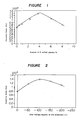
- the coercive forces of the respective media were measured, and the results are shown in Table 2 and in Figure 2. Further, a case where no bias voltage was applied to the substrate is shown as Comparative Example 2.
- Table 2 Substrate bias voltage (V) Coercive force (Oe) Example 7 -50 1150 -100 1380 -150 1290 -200 1100 Comparative Example 2 - 780
- the substrate temperature during the formation of each layer is represented by the substrate temperature immediately prior to the formation of the layer.
- Table 3 Substrate temp. (°C) Coercive force (Oe) 30 800 120 1010 160 1380 200 1480 250 1520
- a magnetic recording medium was produced in the same manner as in Example 1 except that Ni and B chips were mounted on a target having a composition of Co 80 atomic % - Ni 20 atomic % to adjust the composition of the magnetic layer to Co 66.1 atomic % - Ni 31.6 atomic % - B 2.3 atomic %, and a bias voltage of -100 V was applied to the substrate only during the formation of the magnetic layer.
- the coercive force was measured and found to be 1330 Oe.
- This value is slightly smaller than the case where the substrate bias voltage was applied also at the time of forming the Cr primer layer.
- a non-magnetic Ni-P layer was formed by electroless plating in a thickness of 25 ⁇ m on the surface of an aluminum alloy disk substrate having an inner diameter of 25 mm and an outer diameter of 95 mm, and the surface was polished for specular finish to obtain Ra (central line average roughness) of from 20 to 30 ⁇ .
- This non-magnetic substrate was mounted in a high frequency (13.56 MHz) magnetron sputtering apparatus, and the apparatus was evacuated to 1 x 10 ⁇ 6 Torr. Then, the substrate temperature was raised to 160°C, and a Cr primer layer was formed in a thickness of about 1400 ⁇ while applying a direct current bias voltage of -100 V to the substrate.
- the magnetic layer was formed in the same manner as in Example 10 except that the composition of the magnetic layer was adjusted to Co 71.3 atomic % - Ni 17.3 atomic % - Cr 7.7 atomic % - B 3.7 atomic %, and the direct current bias voltage applied to the non-magnetic substrate was changed to the voltage as identified in Table 5.
- the coercive force of each magnetic medium was measured, and the results are shown in Table 5 and in Figure 5.
- Table 5 Substrate bias voltage (V) Coercive force (Oe)
- Example 14 -50 1400 -100 1740 -150 1660 -200 1500 -250 1200 Comparative Example 4 - 1050
- a magnetic recording medium having a magnetic layer with a composition of Co 71.3 atomic % - Ni 17.3 atomic % - Cr 7.7 atomic % - B 3.7 atomic % was produced in the same manner as in Example 10 except that the substrate temperature during the formation of the magnetic layer was adjusted to the temperature identified in Table 6. The coercive force of each magnetic recording medium was measured, and the results are shown in Table 6 and in Figure 6.
- the substrate temperature during the formation of the layer is represented by the substrate temperature immediately prior to the formation of the layer.
- Table 6 Substrate temp. (°C) Coercive force (Oe) 30 940 120 1150 160 1740 200 1980
- a magnetic recording medium was produced in the same manner as in Example 10 except that the composition of the magnetic layer was adjusted to Co 71.3 atomic % - Ni 17.3 atomic % - Cr 7.7 atomic % - B 3.7 atomic %, and the substrate bias voltage of -100 V was applied only during the formation of the magnetic layer.
- the coercive force was measured and found to be 1630 Oe. This value is slightly lower than the case where the substrate bias voltage was applied also during the formation of Cr primer layer.
- a magnetic recording medium was produced in the same manner as in Example 10 except that a target having a various number of B chips mounted on an alloy target for the magnetic layer having a composition of Co 84 atomic % - Cr 16 atomic %, was used.
- the coercive force was measured, and the results are shown in Table 7 together with the composition of the magnetic layer.
- Table 7 Composition of magnetic layer (atomic %) Coercive force (Oe) Co Cr B Comparative Example 5 82.9 15.8 1.3 1080 Comparative Example 6 84.0 16.0 - 1460
- the magnetic recording medium of the present invention is the one wherein a magnetic alloy layer having a specific composition is formed on a non-magnetic substrate with a Cr-type primer layer interposed therebetween.
- a remarkably high coercive force is obtained by applying a negative bias voltage to the non-magnetic substrate when the magnetic layer is formed by sputtering. Accordingly, it is possible to provide a magnetic recording medium useful for high density recording.
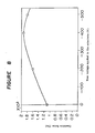
- the magnetic layer was formed in the same manner as in Example 14 except that the composition of the magnetic layer was adjusted to Co 61 atomic % - Ni 29 atomic % - Cr 7 atomic % - B 3 atomic %, a DC magnetron sputtering apparatus was used as the sputtering apparatus, the non-magnetic substrate was heated to 210°C, and the direct current substrate bias voltage was changed to a level as identified in Table 8. The coercive force of each magnetic medium was measured, and the results are shown in Table 8 and Figure 8. Table 8 Substrate bias voltage (V) Coercive force (Oe) Example 17 -200 1600 -400 1940 -500 1800 Comparative Example 7 - 1100
- Example 17 the magnetic layer was formed by using a sputtering apparatus as shown in Figure 7, wherein reference numeral 1 indicates a target, numeral 2 indicates a substrate holder, numeral 3 indicates a substrate, numeral 4 indicates an intermediate electrode, numeral 5 indicates a power source for sputtering, and numeral 6 indicates a power source for the intermediate electrode.
- a positive direct current voltage as identified in Table 9 was applied.
- the coercive force of each magnetic medium was measured, and the results are shown in Table 9 and Figure 9.
- Table 9 Intermediate electrode voltage (V) Coercive force (Oe) Example 18 +100 1320 +200 1650 +300 1850 +400 1750 Comparative Example 8 - 1000
- the magnetic layer was formed in the same manner as in Example 18 except that the composition of the magnetic layer was adjusted to Co 67 atomic % - Ni 30 atomic % - B 3 atomic %. During the layer forming, a current voltage of +300 V was applied to the intermediate electrode. The coercive force was 1380 Oe.
Landscapes
- Engineering & Computer Science (AREA)
- Chemical & Material Sciences (AREA)
- Metallurgy (AREA)
- Inorganic Chemistry (AREA)
- Ceramic Engineering (AREA)
- Manufacturing Of Magnetic Record Carriers (AREA)
Applications Claiming Priority (4)
| Application Number | Priority Date | Filing Date | Title |
|---|---|---|---|
| JP8494589 | 1989-04-04 | ||
| JP8494789 | 1989-04-04 | ||
| JP84947/89 | 1989-04-04 | ||
| JP84945/89 | 1989-04-04 |
Publications (3)
| Publication Number | Publication Date |
|---|---|
| EP0391258A2 true EP0391258A2 (fr) | 1990-10-10 |
| EP0391258A3 EP0391258A3 (fr) | 1991-04-03 |
| EP0391258B1 EP0391258B1 (fr) | 1995-06-14 |
Family
ID=26425914
Family Applications (1)
| Application Number | Title | Priority Date | Filing Date |
|---|---|---|---|
| EP90106058A Expired - Lifetime EP0391258B1 (fr) | 1989-04-04 | 1990-03-29 | Support d'enregistrement magnétique et méthode de fabrication |
Country Status (4)
| Country | Link |
|---|---|
| US (1) | US5492745A (fr) |
| EP (1) | EP0391258B1 (fr) |
| KR (1) | KR0176244B1 (fr) |
| DE (1) | DE69020032D1 (fr) |
Cited By (3)
| Publication number | Priority date | Publication date | Assignee | Title |
|---|---|---|---|---|
| EP0651380A1 (fr) * | 1993-11-03 | 1995-05-03 | Hewlett-Packard Company | Méthode de préparation de supports d'enregistrement pour une unité de disque et support d'enregistrement pour l'unité de disque |
| US5494722A (en) * | 1992-01-29 | 1996-02-27 | Mitsubishi Chemical Corporation | Magnetic recording medium and method for its production |
| EP1693834A1 (fr) * | 2005-02-22 | 2006-08-23 | Fuji Photo Film Co., Ltd. | Moyen d'enregistrement magnétique |
Families Citing this family (16)
| Publication number | Priority date | Publication date | Assignee | Title |
|---|---|---|---|---|
| US6938825B1 (en) * | 1989-04-24 | 2005-09-06 | Ultracard, Inc. | Data system |
| DE19508535A1 (de) * | 1995-03-10 | 1996-09-12 | Leybold Materials Gmbh | Sputtertarget aus einer Kobalt-Basislegierung mit hohem Magnetfelddurchgriff |
| US6022609A (en) * | 1996-10-02 | 2000-02-08 | Seagate Technology, Inc. | Magnetic recording medium with substantially uniform sub-micron-scale morphology |
| DE19720251A1 (de) * | 1997-05-15 | 1998-11-19 | Fraunhofer Ges Forschung | Verfahren zum Beschichten von Dünnfilmmagnetplatten |
| US5968627A (en) * | 1998-01-15 | 1999-10-19 | Flextor, Inc. | Metal foil disk for high areal density recording in environments of high mechanical shock |
| US6871787B1 (en) | 1998-07-10 | 2005-03-29 | Ultracard, Inc. | Data storage card having a glass substrate and data surface region and method for using same |
| US6210819B1 (en) | 1998-07-24 | 2001-04-03 | Hmt Technology Corporation | Magnetic recording media having a CrTi underlayer deposited under a substrate bias |
| US6495252B1 (en) * | 1999-07-22 | 2002-12-17 | Seagate Technology Llc | Magnetic recording medium with superparamagnetic underlayer |
| WO2001016945A1 (fr) | 1999-09-01 | 2001-03-08 | Mitsubishi Chemical Corporation | Support d'enregistrement magnetique et dispositif d'enregistrement magnetique |
| US7487908B1 (en) * | 1999-10-23 | 2009-02-10 | Ultracard, Inc. | Article having an embedded accessible storage member, apparatus and method for using same |
| US8397998B1 (en) | 1999-10-23 | 2013-03-19 | Ultracard, Inc. | Data storage device, apparatus and method for using same |
| US7036739B1 (en) * | 1999-10-23 | 2006-05-02 | Ultracard, Inc. | Data storage device apparatus and method for using same |
| US6969006B1 (en) | 2000-09-15 | 2005-11-29 | Ultracard, Inc. | Rotable portable card having a data storage device, apparatus and method for using same |
| US6709774B2 (en) * | 2001-09-18 | 2004-03-23 | International Business Machines Corporation | Magnetic thin film disks with a nonuniform composition |
| JP4466925B2 (ja) * | 2004-08-10 | 2010-05-26 | 日鉱金属株式会社 | フレキシブル銅基板用バリア膜及びバリア膜形成用スパッタリングターゲット |
| KR102310933B1 (ko) | 2021-03-11 | 2021-10-07 | 남서울대학교 산학협력단 | 자석을 통전용으로 사용한 중공형 방수슬립링 |
Family Cites Families (17)
| Publication number | Priority date | Publication date | Assignee | Title |
|---|---|---|---|---|
| DE2542201A1 (de) * | 1975-09-22 | 1977-03-31 | Siemens Ag | Verfahren zur herstellung von platten fuer die speicherung von videosignalen |
| JPS56148729A (en) * | 1980-04-21 | 1981-11-18 | Fuji Photo Film Co Ltd | Magnetic recording medium |
| JPS5961014A (ja) * | 1982-09-29 | 1984-04-07 | Fuji Photo Film Co Ltd | 磁気記録媒体 |
| JPS60113320A (ja) * | 1983-11-22 | 1985-06-19 | Nec Corp | 記録体基板およびその製造方法 |
| EP0154158B1 (fr) * | 1984-02-02 | 1988-10-19 | Hitachi Metals, Ltd. | Procédé pour la fabrication de supports d'enregistrement magnétique |
| EP0182367B1 (fr) * | 1984-11-20 | 1990-04-18 | Hitachi Maxell Ltd. | Milieu d'enregistrement magnétique et sa fabrication |
| EP0205239A3 (fr) * | 1985-05-03 | 1987-11-19 | Akashic Memories Corporation | Disque magnétique à couche mince |
| US4769282A (en) * | 1985-06-21 | 1988-09-06 | Sumitomo Metal Mining Co., Ltd. | Magnetic recording medium |
| JPS62112226A (ja) * | 1985-11-11 | 1987-05-23 | Sony Corp | 垂直磁気記録媒体の製造方法 |
| JPS62141628A (ja) * | 1985-12-16 | 1987-06-25 | Fuji Electric Co Ltd | 磁気記録媒体 |
| US4755426A (en) * | 1986-01-18 | 1988-07-05 | Hitachi Maxell, Ltd. | Magnetic recording medium and production of the same |
| JPS62242324A (ja) * | 1986-04-14 | 1987-10-22 | 松下電器産業株式会社 | チツプコンデンサ− |
| JPS6326827A (ja) * | 1986-07-21 | 1988-02-04 | Hitachi Ltd | 磁気記録媒体の製造方法 |
| JPS63149848A (ja) * | 1986-12-12 | 1988-06-22 | Matsushita Electric Ind Co Ltd | 光磁気デイスク製造装置 |
| JPS63162090A (ja) * | 1986-12-24 | 1988-07-05 | Hitachi Ltd | 水棲生物の附着汚損を防止する装置 |
| EP0303324A1 (fr) * | 1987-08-10 | 1989-02-15 | Koninklijke Philips Electronics N.V. | Matériau magnétique, son procédé de fabrication et tête magnétique munie de ce matériau |
| KR970002340B1 (ko) * | 1988-07-15 | 1997-03-03 | 미쓰비시 가세이 가부시끼가이샤 | 자기 기록 매체의 제조방법 |
-
1990
- 1990-03-29 DE DE69020032T patent/DE69020032D1/de not_active Expired - Lifetime
- 1990-03-29 EP EP90106058A patent/EP0391258B1/fr not_active Expired - Lifetime
- 1990-04-04 KR KR1019900004669A patent/KR0176244B1/ko not_active Expired - Fee Related
-
1994
- 1994-02-10 US US08/194,636 patent/US5492745A/en not_active Expired - Lifetime
Cited By (3)
| Publication number | Priority date | Publication date | Assignee | Title |
|---|---|---|---|---|
| US5494722A (en) * | 1992-01-29 | 1996-02-27 | Mitsubishi Chemical Corporation | Magnetic recording medium and method for its production |
| EP0651380A1 (fr) * | 1993-11-03 | 1995-05-03 | Hewlett-Packard Company | Méthode de préparation de supports d'enregistrement pour une unité de disque et support d'enregistrement pour l'unité de disque |
| EP1693834A1 (fr) * | 2005-02-22 | 2006-08-23 | Fuji Photo Film Co., Ltd. | Moyen d'enregistrement magnétique |
Also Published As
| Publication number | Publication date |
|---|---|
| DE69020032D1 (de) | 1995-07-20 |
| KR0176244B1 (ko) | 1999-04-15 |
| KR900016953A (ko) | 1990-11-14 |
| US5492745A (en) | 1996-02-20 |
| EP0391258B1 (fr) | 1995-06-14 |
| EP0391258A3 (fr) | 1991-04-03 |
Similar Documents
| Publication | Publication Date | Title |
|---|---|---|
| EP0391258B1 (fr) | Support d'enregistrement magnétique et méthode de fabrication | |
| EP0388088A2 (fr) | Disque magnétique pour stocker des dates à bas niveau intrinsèque de bruit | |
| US5851688A (en) | Thin film magnetic alloy having low noise, high coercivity, and high squareness | |
| US5736262A (en) | Magnetic recording medium | |
| US4642270A (en) | Magnetic recording medium | |
| EP0350940B1 (fr) | Procédé et dispositif pour la fabrication d'un milieu d'enregistrement magnétique | |
| US5494722A (en) | Magnetic recording medium and method for its production | |
| EP0008328B1 (fr) | Films magnétiques amorphes et procédé pour leur fabrication | |
| EP0247868B1 (fr) | Film magnétique et tête magnétique l'utilisant | |
| US5834111A (en) | Multilayered magnetic recording medium with coercivity gradient | |
| US5084152A (en) | Method for preparing high density magnetic recording medium | |
| EP0576376B1 (fr) | Film magnétique cobalt-platine et méthode de fabrication | |
| US4735853A (en) | Magnetic recording medium having an amorphous, nonmagnetic nickel-tungston-phosphorus underlayer | |
| US5552217A (en) | Magnetic recording medium and a method for producing it | |
| EP0505783B1 (fr) | Milieu d'enregistrement magnétique | |
| JPH0647722B2 (ja) | 磁気記録媒体の製造方法 | |
| US4753852A (en) | Magnetic recording medium comprising a magnetic Co-Ni-Cr alloy thin layer | |
| JPH0349021A (ja) | 磁気記録媒体及びその製造方法 | |
| JPH0354723A (ja) | 磁気記録媒体及びその製造方法 | |
| EP0183120B1 (fr) | Elément d'enregistrement magnétique | |
| KR920008436B1 (ko) | 자기기록체 | |
| JP2814623B2 (ja) | 磁気記録媒体及びその製造方法 | |
| KR0164459B1 (ko) | 코발트 페라이트 자성 박막 및 그 제조방법 | |
| EP0513418A1 (fr) | Milieu d'enregistrement magnétique | |
| JP2832941B2 (ja) | 面内磁気記録媒体 |
Legal Events
| Date | Code | Title | Description |
|---|---|---|---|
| PUAI | Public reference made under article 153(3) epc to a published international application that has entered the european phase |
Free format text: ORIGINAL CODE: 0009012 |
|
| AK | Designated contracting states |
Kind code of ref document: A2 Designated state(s): DE GB IT |
|
| 17P | Request for examination filed |
Effective date: 19901212 |
|
| PUAL | Search report despatched |
Free format text: ORIGINAL CODE: 0009013 |
|
| AK | Designated contracting states |
Kind code of ref document: A3 Designated state(s): DE GB IT |
|
| 17Q | First examination report despatched |
Effective date: 19930526 |
|
| RAP1 | Party data changed (applicant data changed or rights of an application transferred) |
Owner name: MITSUBISHI CHEMICAL CORPORATION |
|
| GRAA | (expected) grant |
Free format text: ORIGINAL CODE: 0009210 |
|
| AK | Designated contracting states |
Kind code of ref document: B1 Designated state(s): DE GB IT |
|
| PG25 | Lapsed in a contracting state [announced via postgrant information from national office to epo] |
Ref country code: IT Free format text: LAPSE BECAUSE OF FAILURE TO SUBMIT A TRANSLATION OF THE DESCRIPTION OR TO PAY THE FEE WITHIN THE PRESCRIBED TIME-LIMIT;WARNING: LAPSES OF ITALIAN PATENTS WITH EFFECTIVE DATE BEFORE 2007 MAY HAVE OCCURRED AT ANY TIME BEFORE 2007. THE CORRECT EFFECTIVE DATE MAY BE DIFFERENT FROM THE ONE RECORDED. Effective date: 19950614 |
|
| REF | Corresponds to: |
Ref document number: 69020032 Country of ref document: DE Date of ref document: 19950720 |
|
| PG25 | Lapsed in a contracting state [announced via postgrant information from national office to epo] |
Ref country code: DE Effective date: 19950915 |
|
| PLBE | No opposition filed within time limit |
Free format text: ORIGINAL CODE: 0009261 |
|
| STAA | Information on the status of an ep patent application or granted ep patent |
Free format text: STATUS: NO OPPOSITION FILED WITHIN TIME LIMIT |
|
| 26N | No opposition filed | ||
| PGFP | Annual fee paid to national office [announced via postgrant information from national office to epo] |
Ref country code: GB Payment date: 19990401 Year of fee payment: 10 |
|
| PG25 | Lapsed in a contracting state [announced via postgrant information from national office to epo] |
Ref country code: GB Free format text: LAPSE BECAUSE OF NON-PAYMENT OF DUE FEES Effective date: 20000329 |
|
| GBPC | Gb: european patent ceased through non-payment of renewal fee |
Effective date: 20000329 |