EP0391671A2 - Elektro-optisches Sender-Empfänger-Bauelement in einem Gehäuse - Google Patents
Elektro-optisches Sender-Empfänger-Bauelement in einem Gehäuse Download PDFInfo
- Publication number
- EP0391671A2 EP0391671A2 EP90303570A EP90303570A EP0391671A2 EP 0391671 A2 EP0391671 A2 EP 0391671A2 EP 90303570 A EP90303570 A EP 90303570A EP 90303570 A EP90303570 A EP 90303570A EP 0391671 A2 EP0391671 A2 EP 0391671A2
- Authority
- EP
- European Patent Office
- Prior art keywords
- light source
- photosensitive device
- variable light
- lead
- lense
- Prior art date
- Legal status (The legal status is an assumption and is not a legal conclusion. Google has not performed a legal analysis and makes no representation as to the accuracy of the status listed.)
- Granted
Links
Images
Classifications
-
- H—ELECTRICITY
- H10—SEMICONDUCTOR DEVICES; ELECTRIC SOLID-STATE DEVICES NOT OTHERWISE PROVIDED FOR
- H10F—INORGANIC SEMICONDUCTOR DEVICES SENSITIVE TO INFRARED RADIATION, LIGHT, ELECTROMAGNETIC RADIATION OF SHORTER WAVELENGTH OR CORPUSCULAR RADIATION
- H10F55/00—Radiation-sensitive semiconductor devices covered by groups H10F10/00, H10F19/00 or H10F30/00 being structurally associated with electric light sources and electrically or optically coupled thereto
- H10F55/20—Radiation-sensitive semiconductor devices covered by groups H10F10/00, H10F19/00 or H10F30/00 being structurally associated with electric light sources and electrically or optically coupled thereto wherein the electric light source controls the radiation-sensitive semiconductor devices, e.g. optocouplers
- H10F55/25—Radiation-sensitive semiconductor devices covered by groups H10F10/00, H10F19/00 or H10F30/00 being structurally associated with electric light sources and electrically or optically coupled thereto wherein the electric light source controls the radiation-sensitive semiconductor devices, e.g. optocouplers wherein the radiation-sensitive devices and the electric light source are all semiconductor devices
-
- H—ELECTRICITY
- H03—ELECTRONIC CIRCUITRY
- H03K—PULSE TECHNIQUE
- H03K17/00—Electronic switching or gating, i.e. not by contact-making and –breaking
- H03K17/51—Electronic switching or gating, i.e. not by contact-making and –breaking characterised by the components used
- H03K17/78—Electronic switching or gating, i.e. not by contact-making and –breaking characterised by the components used using opto-electronic devices, i.e. light-emitting and photoelectric devices electrically- or optically-coupled
- H03K17/795—Electronic switching or gating, i.e. not by contact-making and –breaking characterised by the components used using opto-electronic devices, i.e. light-emitting and photoelectric devices electrically- or optically-coupled controlling bipolar transistors
-
- H—ELECTRICITY
- H03—ELECTRONIC CIRCUITRY
- H03K—PULSE TECHNIQUE
- H03K17/00—Electronic switching or gating, i.e. not by contact-making and –breaking
- H03K17/51—Electronic switching or gating, i.e. not by contact-making and –breaking characterised by the components used
- H03K17/78—Electronic switching or gating, i.e. not by contact-making and –breaking characterised by the components used using opto-electronic devices, i.e. light-emitting and photoelectric devices electrically- or optically-coupled
- H03K17/795—Electronic switching or gating, i.e. not by contact-making and –breaking characterised by the components used using opto-electronic devices, i.e. light-emitting and photoelectric devices electrically- or optically-coupled controlling bipolar transistors
- H03K17/7955—Electronic switching or gating, i.e. not by contact-making and –breaking characterised by the components used using opto-electronic devices, i.e. light-emitting and photoelectric devices electrically- or optically-coupled controlling bipolar transistors using phototransistors
-
- H—ELECTRICITY
- H03—ELECTRONIC CIRCUITRY
- H03K—PULSE TECHNIQUE
- H03K17/00—Electronic switching or gating, i.e. not by contact-making and –breaking
- H03K17/94—Electronic switching or gating, i.e. not by contact-making and –breaking characterised by the way in which the control signals are generated
-
- H—ELECTRICITY
- H03—ELECTRONIC CIRCUITRY
- H03K—PULSE TECHNIQUE
- H03K17/00—Electronic switching or gating, i.e. not by contact-making and –breaking
- H03K17/94—Electronic switching or gating, i.e. not by contact-making and –breaking characterised by the way in which the control signals are generated
- H03K17/941—Electronic switching or gating, i.e. not by contact-making and –breaking characterised by the way in which the control signals are generated using an optical detector
-
- H—ELECTRICITY
- H10—SEMICONDUCTOR DEVICES; ELECTRIC SOLID-STATE DEVICES NOT OTHERWISE PROVIDED FOR
- H10W—GENERIC PACKAGES, INTERCONNECTIONS, CONNECTORS OR OTHER CONSTRUCTIONAL DETAILS OF DEVICES COVERED BY CLASS H10
- H10W72/00—Interconnections or connectors in packages
- H10W72/50—Bond wires
- H10W72/531—Shapes of wire connectors
- H10W72/5363—Shapes of wire connectors the connected ends being wedge-shaped
-
- H—ELECTRICITY
- H10—SEMICONDUCTOR DEVICES; ELECTRIC SOLID-STATE DEVICES NOT OTHERWISE PROVIDED FOR
- H10W—GENERIC PACKAGES, INTERCONNECTIONS, CONNECTORS OR OTHER CONSTRUCTIONAL DETAILS OF DEVICES COVERED BY CLASS H10
- H10W74/00—Encapsulations, e.g. protective coatings
- H10W74/10—Encapsulations, e.g. protective coatings characterised by their shape or disposition
-
- H—ELECTRICITY
- H10—SEMICONDUCTOR DEVICES; ELECTRIC SOLID-STATE DEVICES NOT OTHERWISE PROVIDED FOR
- H10W—GENERIC PACKAGES, INTERCONNECTIONS, CONNECTORS OR OTHER CONSTRUCTIONAL DETAILS OF DEVICES COVERED BY CLASS H10
- H10W90/00—Package configurations
- H10W90/701—Package configurations characterised by the relative positions of pads or connectors relative to package parts
- H10W90/751—Package configurations characterised by the relative positions of pads or connectors relative to package parts of bond wires
- H10W90/756—Package configurations characterised by the relative positions of pads or connectors relative to package parts of bond wires between a chip and a stacked lead frame, conducting package substrate or heat sink
Definitions
- This invention concerns electro-optic transmitter-receivers and, more particularly, a single package, a series connected semiconductor electro-optic transmitter-receiver in which both emitter and receiver face outwardly through a transparent cover.
- the emitter is a light emitting semiconductor diode (LED) which emits light when energized.
- the light from the LED travels through the transparent cover and exits the device package where it may encounter a separate receiver device or an object that returns part of the emitted light back through the transparent cover to the receiver device in the same housing.
- Phototransistors, photodiodes and photoresistors are well known receiver devices. It is important that the wavelength sensitivity of the receiver device be such that it can reasonably detect the light wavelength emitted by the LED or other optical emitter within the housing.
- Prior art devices suffer from a number of disadvantages, such as for example, use of complex and expensive semiconductor devices and/or housings which increase manufacturing cost and/or fail to provide the desired performance.
- a single package, emitter-receiver device comprising, a lead means having thereon an outwardly projecting variable light source and an outwardly directed photosensitive device, and a transparent cover means for allowing passage of light located over the photosensitive device and variable light source, wherein the cover means desirably has a convexly curved lense means substantially centrally located over the photosensitive device for collecting light and a flat or concave portion located over the variable light source for transmitting light.
- the photosensitive device and the variable light source and lead means are arranged so that, absent reflection or scattering external to the device, light from the variable light source backscattered within the packages is insufficient to turn on the photosensitive device.
- the photosensitive device is mounted on a first portion of the lead means and the variable light source is mounted on a second, spaced apart portion of the lead means.
- the lead means comprises a first portion having thereon the photosensitive device, a second portion having thereon the variable light source and a third portion, wherein the first, second and third portions are spaced apart in a substantially common plane.
- a first electrical interconnection means desirably extends between the variable light source and the first portion of the lead means and a second electrical interconnection means desirably extends between the third portion of the lead means and the photosensitive device.
- the photosensitive device is a phototransistor having its collector bonded to the first portion of the lead means and its emitter coupled to the third portion of the lead means and the variable light source is an LED having one terminal bonded to the second portion of the lead means and another terminal coupled to the first portion of the lead means.
- the curved lense means is recessed within the transparent cover means so as to not protrude therefrom.
- the curved lense means and flat or concave portion of the transparent cover means are desirably unitary.
- the photosensitive device is mounted on a first portion of the lead means and the variable light source is mounted on the same portion of the lead means, but spaced-apart from the photosensitive device.
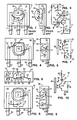
- FIG. 1 is a simplified top view and FIG. 2 a simplified side view of single package semiconductor emitter-receiver 10 according to the prior art.
- Emitter-receiver 10 comprises leads 12, 14, 16 enclosed within cover 18.
- Central lead 14 has die bond portion 20 on which are mounted phototransistor 22 and LED 24.
- Wirebond 23 connects phototransistor 22 to lead 16 and wirebond 25 connects LED 24 to lead 12.
- Cover 18 has protruding transparent convex lense 19 located over both phototransistor 22 and LED 24. In this fashion, light 26 emitted by LED 24 and light 28 received by phototransistor 22 pass through lense 19.
- GaAs LED's are suitable for use in connection with silicon receivers, as for example silicon based phototransistors. Such devices are well known in the art and means for assembling such are also well known.
- FIG. 3 shows a circuit diagram in which a pair of identical prior art devices 10, 10′ of FIGS. 1-2 comprising transistors 22, 22′ and LED's 24, 24′, are arranged emitter to receiver across gap 30.
- LED current limiting resistors 32, 32′ and output resistors 34, 34′ are provided. Power is applied between leads 16, 16′ and ground. There need not be any common electrical connection between circuits 10, 10′, only the optical connection across gap 30.
- a difficulty associated with the arrangement of FIGS. 1-2 is that both the LED and phototransistor are located in close proximity so as to be under the same lense. This increases the likelihood of crosstalk, i.e., light from LED 24 unintentionally reaching phototransistor 22 through internal backscattering within the package.
- the signaling arrangement shown schematically in FIG. 3 cannot run in a duplex mode, i.e., devices 10 and 10′ transmitting and receiving simultaneously, but must run only in a simplex mode, i.e., device 10 transmitting and device 10′ receiving or vice versa, but not both at the same time.
- a further difficulty with the device of FIGS. 1-2 is that, where an NPN phototransistor is desired to be used, then a P-substrate LED must be provided so that the LED can be arranged in the correct electrical direction on common bonding portion 20. P-substrate LED's are often less desirable than N-substrate LED's because of their higher cost.
- FIGS. 4-6 show, respectively, a simplified top view, side view, and front view of single package semiconductor emitter-receiver 40 according to the present invention.
- Emitter-receiver 40 comprises leads 42, 44, 46 enclosed within cover 48.
- Central lead 44 has die bond portion 50 on which is mounted phototransistor 52 so that, for example, the collector thereof is in electrical contact with lead 44.
- LED 54 is mounted on lead 42 so that, for example, the anode of LED 54 is in electrical contact with lead 42.
- Wirebond 53 connects, for example, the emitter of phototransistor 52 to lead 46 and wirebond 55 connects, for example, the anode of LED 54 to lead 44.
- Transparent cover 48 has convex lense 49 centrally located over phototransistor 52 but not over LED 54. Light 58 received by phototransistor 52 passes centrally through lense 49, but light 56 emitted by LED 54 does not.
- This provides improved light collection efficiency for phototransistor 52 as compared to the prior art arrangement of FIGS. 1-2 in which phototransistor 22 is not centrally located under lense 19, but is located to one side in order to leave space for LED 24 which shares lense 19.
- Lense 49 may protrude in a fashion analogous to lense 19 of FIGS. 1-2. However, the recessed arrangement of lense 49 shown in FIGS. 4-6 is preferred since it makes lense 49 less susceptible to surface damage which adversely affects device performance. For example, surface scratches on protruding lense 19 of FIGS. 1-2 can significantly increase the amount of internal light backscattering.
- FIGS. 4-6 While a convex lense may also be provided over LED 54, in a preferred embodiment, light 56 from LED 54 passes through substantially flat or concave (dotted) surface portion 59 of transparent cover 48.
- the preferred structure is particularly simple to manufacture and has been found to give improved results compared to the prior art device of FIGS. 1-2. With surface portion 59 of cover 48 above LED 54 substantially flat, broader external light dispersion was obtained. Also, the arrangement of FIGS. 4-6 is less susceptible to internal light backscatter from LED 54 affecting transistor 52.
- surface portion 49′ of lense 49 extending into body 48 acts as a built-in optical separator that impedes transmission of internally scattered light from LED 42 to transistor 52, such as for example, light that is back-scattered from the body-air interface at surface portion 59.
- the placement of object 60 with respect to emitter-receiver 40 is less critical and a greater on-off signal ratio is obtained from transistor 52 for the same exitation level on LED 54, as object 60 is inserted or removed from the path of emitted light 56.
- this is because the invented arrangement of FIGS. 4-6 has lower levels of internal light backscattering than the prior art arrangement of FIGS. 1-2.
- FIGS. 8-10 show, respectively, a simplified top view and side view of single package semiconductor emitter-receiver 60 and FIG. 10 shows a simplified schematic diagram applicable to the device of FIGS. 8-9.
- Emitter-receiver 60 comprises leads 62, 64, 66 enclosed within cover 68.
- Central lead 64 has die bond portion 70 on which is mounted phototransistor 72 so that, for example, the collector thereof is in electrical contact with lead 64.
- LED 74 is mounted elsewhere on die bond portion 70 or elsewhere on lead 64 so that, for example, the cathode of LED 74 is in electrical contact with lead 64.
- Wirebond 73 connects, for example, the emitter of phototransistor 72 to lead 66 and wirebond 75 connects, for example, the anode of LED 74 to lead 62.
- Transparent cover 68 has convex lense 69 centrally located over phototransistor 72 but not over LED 74.
- Light 78 received by phototransistor 72 passes centrally through lense 69, but light 76 emitted by LED 74 does not.
- a convex lense may also be provided over LED 74, in a preferred embodiment, light 76 from LED 74 passes through substantially flat or concave (dotted) portion 79 of transparent cover 68. This arrangement has the advantages already described in connection with FIGS. 4-6, including recessed surface portion 69′ between LED 74 and photo-transistor 72.
- FIG. 10 illustrates how the device of FIGS. 8-9 may be connected to resistors 82, 84.
- Light 76 from LED 74 is reflected or scattered as light 78 from object 80 back to phototransistor 72 when object 80 is in the path of light 76. Otherwise there is substantially no optical path between LED 74 and transistor 72.
- a feature of the arrangement of FIG. 10 is that it is regenerative, that is, as the impedance of phototransistor 72 decreases in response to receiving reflected or scattered light 58, the current through LED 74 also increases causing an increase in emitted light 76. Other things being equal, this increase in emitted light 76 increases received light 78, further reducing the impedance of transistor 72. This regenerative action continues until phototransistor 72 is in saturation where it will remain until object 80 is removed or the light path otherwise interrupted so that the reflected or scattered light drops below the level necessary to sustain conduction in transistor 72. The circuit then shuts off. This circuit has the advantage of a snap-action due to the regeneration and a larger on-off signal ratio that would be obtainable without the regenerative feedback.
- the substantially flat leadframe employed in the preferred implementation of the present invention is easy to manufacture by means well known in the art and is easy to handle in assembly, as compared to other types of leadframes commonly employed with optoelectronic components.
- Both the LED and the phototransistor are mounted on flat portions of the leadframe which lie substantially in the same plane. Although various parts of the leadframe might be down-formed or up-formed, this is not necessary.
- the LED and phototransistor are conveniently in the form of die having one contact which is made to the surface on which they are mounted and which are attached to the leadframe by means well known in the art. It is not necessary to use insulators on the leadframe to isolate either the LED or the phototransistor therefrom.
- the simple, back-contact die and planar leadframe of the preferred embodiment of the present invention is especially well suited for low cost automated assembly. Hence the invented product may be produced particularly economically.
Landscapes
- Photo Coupler, Interrupter, Optical-To-Optical Conversion Devices (AREA)
Applications Claiming Priority (2)
| Application Number | Priority Date | Filing Date | Title |
|---|---|---|---|
| US07/331,712 US4972089A (en) | 1989-04-03 | 1989-04-03 | Single package electro-optic transmitter-receiver |
| US331712 | 1989-04-03 |
Publications (3)
| Publication Number | Publication Date |
|---|---|
| EP0391671A2 true EP0391671A2 (de) | 1990-10-10 |
| EP0391671A3 EP0391671A3 (de) | 1991-01-30 |
| EP0391671B1 EP0391671B1 (de) | 1994-12-21 |
Family
ID=23295053
Family Applications (1)
| Application Number | Title | Priority Date | Filing Date |
|---|---|---|---|
| EP90303570A Expired - Lifetime EP0391671B1 (de) | 1989-04-03 | 1990-04-03 | Elektro-optisches Sender-Empfänger-Bauelement in einem Gehäuse |
Country Status (5)
| Country | Link |
|---|---|
| US (1) | US4972089A (de) |
| EP (1) | EP0391671B1 (de) |
| JP (1) | JP2969761B2 (de) |
| KR (1) | KR0153000B1 (de) |
| DE (1) | DE69015236T2 (de) |
Cited By (1)
| Publication number | Priority date | Publication date | Assignee | Title |
|---|---|---|---|---|
| EP1528358A1 (de) * | 2003-10-29 | 2005-05-04 | Leica Geosystems AG | Optisches Bauteil und Verfahren zu dessen Herstellung |
Families Citing this family (23)
| Publication number | Priority date | Publication date | Assignee | Title |
|---|---|---|---|---|
| US5130531A (en) * | 1989-06-09 | 1992-07-14 | Omron Corporation | Reflective photosensor and semiconductor light emitting apparatus each using micro Fresnel lens |
| US5091642A (en) * | 1990-05-11 | 1992-02-25 | Mda Scientific, Inc. | Colorimetric detection apparatus |
| JP2974469B2 (ja) * | 1991-09-17 | 1999-11-10 | 株式会社東芝 | 信号伝送回路 |
| US5317149A (en) * | 1992-11-12 | 1994-05-31 | Hewlett-Packard Company | Optical encoder with encapsulated electrooptics |
| US5340993A (en) * | 1993-04-30 | 1994-08-23 | Motorola, Inc. | Optocoupler package wth integral voltage isolation barrier |
| DE69421884T2 (de) * | 1993-09-30 | 2000-05-11 | Siemens Components, Inc. | Linearer bidirektionaler Optokoppler |
| JP2000082829A (ja) * | 1998-09-04 | 2000-03-21 | Dowa Mining Co Ltd | 受光方法及び受光装置並びに受発光装置 |
| US6679608B2 (en) * | 1999-01-25 | 2004-01-20 | Gentex Corporation | Sensor device having an integral anamorphic lens |
| US6485354B1 (en) * | 2000-06-09 | 2002-11-26 | Strasbaugh | Polishing pad with built-in optical sensor |
| US6590269B1 (en) * | 2002-04-01 | 2003-07-08 | Kingpak Technology Inc. | Package structure for a photosensitive chip |
| DE10259185A1 (de) * | 2002-12-18 | 2004-07-15 | Daimlerchrysler Ag | Multifunktionale Beleuchtungseinrichtung |
| DE10346474B4 (de) * | 2003-10-02 | 2014-07-10 | Infineon Technologies Ag | Sensorbauteil mit einem Sensorchip, Sensorstapel und Verfahren zum Prüfen einer biochemischen Probe |
| DE10355371A1 (de) * | 2003-11-25 | 2005-06-23 | Ion Ag | Verfahren zur Visualisierung, Bewertung und Ermittlung von Prozessgrößen |
| US9070850B2 (en) | 2007-10-31 | 2015-06-30 | Cree, Inc. | Light emitting diode package and method for fabricating same |
| US7482666B2 (en) * | 2006-01-12 | 2009-01-27 | Silicon Laboratories Inc. | Apparatus and method for optical isolation |
| GB201020024D0 (en) | 2010-11-25 | 2011-01-12 | St Microelectronics Ltd | Radiation sensor |
| GB201020023D0 (en) | 2010-11-25 | 2011-01-12 | St Microelectronics Ltd | Radiation sensor |
| GB2486000A (en) * | 2010-11-30 | 2012-06-06 | St Microelectronics Res & Dev | Optical proximity detectors with arrangements for reducing internal light propagation from emitter to detector |
| GB2485998A (en) | 2010-11-30 | 2012-06-06 | St Microelectronics Res & Dev | A single-package optical proximity detector with an internal light baffle |
| GB2485996A (en) | 2010-11-30 | 2012-06-06 | St Microelectronics Res & Dev | A combined proximity and ambient light sensor |
| JP6094361B2 (ja) * | 2013-04-24 | 2017-03-15 | オムロン株式会社 | フォトセンサ |
| US10622522B2 (en) * | 2014-09-05 | 2020-04-14 | Theodore Lowes | LED packages with chips having insulated surfaces |
| DE102016103136A1 (de) * | 2016-02-23 | 2017-08-24 | Vishay Semiconductor Gmbh | Optoelektronische Vorrichtung |
Family Cites Families (10)
| Publication number | Priority date | Publication date | Assignee | Title |
|---|---|---|---|---|
| FR2106710A5 (de) * | 1970-09-22 | 1972-05-05 | Radiotechnique Compelec | |
| US3842263A (en) * | 1973-02-01 | 1974-10-15 | Gen Electric | Molded opto-electronic transducer |
| US4309605A (en) * | 1979-10-02 | 1982-01-05 | New Japan Radio Co., Ltd. | Photo-reflective sensor |
| JPS57139976A (en) * | 1981-02-23 | 1982-08-30 | Omron Tateisi Electronics Co | Light emitting/receiving device |
| JPS5889887A (ja) * | 1981-11-25 | 1983-05-28 | Univ Tohoku | 半導体光機能デバイス |
| US4794431A (en) * | 1986-04-21 | 1988-12-27 | International Rectifier Corporation | Package for photoactivated semiconductor device |
| JPS63176A (ja) * | 1986-06-19 | 1988-01-05 | Honda Motor Co Ltd | 複合型光センサ |
| DE3633251A1 (de) * | 1986-09-30 | 1988-03-31 | Siemens Ag | Optoelektronisches koppelelement |
| JPS63104486A (ja) * | 1986-10-22 | 1988-05-09 | Nec Corp | 反射型光センサ− |
| EP0363520A1 (de) * | 1988-10-14 | 1990-04-18 | Wako Corporation | Photoelektrischer Detektor |
-
1989
- 1989-04-03 US US07/331,712 patent/US4972089A/en not_active Expired - Lifetime
-
1990
- 1990-03-30 KR KR1019900004282A patent/KR0153000B1/ko not_active Expired - Fee Related
- 1990-03-31 JP JP8733490A patent/JP2969761B2/ja not_active Expired - Fee Related
- 1990-04-03 DE DE69015236T patent/DE69015236T2/de not_active Expired - Fee Related
- 1990-04-03 EP EP90303570A patent/EP0391671B1/de not_active Expired - Lifetime
Cited By (2)
| Publication number | Priority date | Publication date | Assignee | Title |
|---|---|---|---|---|
| EP1528358A1 (de) * | 2003-10-29 | 2005-05-04 | Leica Geosystems AG | Optisches Bauteil und Verfahren zu dessen Herstellung |
| US7193792B2 (en) | 2003-10-29 | 2007-03-20 | Leica Geosystems Ag | Optical component and method for its production |
Also Published As
| Publication number | Publication date |
|---|---|
| DE69015236T2 (de) | 1995-07-20 |
| JP2969761B2 (ja) | 1999-11-02 |
| EP0391671B1 (de) | 1994-12-21 |
| US4972089A (en) | 1990-11-20 |
| DE69015236D1 (de) | 1995-02-02 |
| KR900017310A (ko) | 1990-11-16 |
| JPH02295176A (ja) | 1990-12-06 |
| KR0153000B1 (ko) | 1998-11-16 |
| EP0391671A3 (de) | 1991-01-30 |
Similar Documents
| Publication | Publication Date | Title |
|---|---|---|
| US4972089A (en) | Single package electro-optic transmitter-receiver | |
| US5654559A (en) | Optical coupling device and method for manufacturing the same | |
| US20010035492A1 (en) | Reflected light barrier | |
| US7290942B2 (en) | Optical transceiver modules | |
| US6678292B2 (en) | Top contact VCSEL with monitor | |
| JPH06209124A (ja) | 狭い開口角を持つ光電子装置 | |
| JP2002076376A (ja) | 光受信装置および光送信装置 | |
| CN101276028B (zh) | 光学半导体模块和受光组件 | |
| US7777234B2 (en) | Light-receiving element and photonic semiconductor device provided therewith | |
| WO2018105358A1 (ja) | フォトカプラ | |
| US20040141699A1 (en) | Optical module | |
| JP3467174B2 (ja) | 光結合素子 | |
| JPS6316682A (ja) | 樹脂封止型発光モジユ−ル | |
| GB2349740A (en) | Vertical cavity surface emitting laser with monitoring diode | |
| JPS6213088A (ja) | 発光半導体装置 | |
| US20250194285A1 (en) | Photocoupler | |
| JP2003177287A (ja) | 光受信モジュール | |
| JP3622460B2 (ja) | 半導体リレー | |
| JPH06232445A (ja) | 光学素子および透過型光結合装置 | |
| JPS6123426A (ja) | 半導体受発光装置 | |
| JPH07244231A (ja) | 光結合装置及び半導体発光素子並びに継電器 | |
| JP3318083B2 (ja) | 半導体レーザ装置 | |
| CN116845060A (zh) | 红外模组和电子设备 | |
| JPH05274967A (ja) | 光電スイッチ | |
| JP3660305B2 (ja) | 半導体レーザ装置の製造方法 |
Legal Events
| Date | Code | Title | Description |
|---|---|---|---|
| PUAI | Public reference made under article 153(3) epc to a published international application that has entered the european phase |
Free format text: ORIGINAL CODE: 0009012 |
|
| AK | Designated contracting states |
Kind code of ref document: A2 Designated state(s): DE FR GB IT |
|
| PUAL | Search report despatched |
Free format text: ORIGINAL CODE: 0009013 |
|
| AK | Designated contracting states |
Kind code of ref document: A3 Designated state(s): DE FR GB IT |
|
| 17P | Request for examination filed |
Effective date: 19910307 |
|
| 17Q | First examination report despatched |
Effective date: 19920928 |
|
| 18D | Application deemed to be withdrawn |
Effective date: 19930105 |
|
| D18D | Application deemed to be withdrawn (deleted) | ||
| GRAA | (expected) grant |
Free format text: ORIGINAL CODE: 0009210 |
|
| ITF | It: translation for a ep patent filed | ||
| AK | Designated contracting states |
Kind code of ref document: B1 Designated state(s): DE FR GB IT |
|
| REF | Corresponds to: |
Ref document number: 69015236 Country of ref document: DE Date of ref document: 19950202 |
|
| ET | Fr: translation filed | ||
| PLBE | No opposition filed within time limit |
Free format text: ORIGINAL CODE: 0009261 |
|
| STAA | Information on the status of an ep patent application or granted ep patent |
Free format text: STATUS: NO OPPOSITION FILED WITHIN TIME LIMIT |
|
| 26N | No opposition filed | ||
| PGFP | Annual fee paid to national office [announced via postgrant information from national office to epo] |
Ref country code: GB Payment date: 19960412 Year of fee payment: 7 |
|
| PGFP | Annual fee paid to national office [announced via postgrant information from national office to epo] |
Ref country code: FR Payment date: 19960426 Year of fee payment: 7 |
|
| PGFP | Annual fee paid to national office [announced via postgrant information from national office to epo] |
Ref country code: DE Payment date: 19960429 Year of fee payment: 7 |
|
| PG25 | Lapsed in a contracting state [announced via postgrant information from national office to epo] |
Ref country code: GB Effective date: 19970403 |
|
| GBPC | Gb: european patent ceased through non-payment of renewal fee |
Effective date: 19970403 |
|
| PG25 | Lapsed in a contracting state [announced via postgrant information from national office to epo] |
Ref country code: FR Free format text: LAPSE BECAUSE OF NON-PAYMENT OF DUE FEES Effective date: 19971231 |
|
| PG25 | Lapsed in a contracting state [announced via postgrant information from national office to epo] |
Ref country code: DE Free format text: LAPSE BECAUSE OF NON-PAYMENT OF DUE FEES Effective date: 19980101 |
|
| REG | Reference to a national code |
Ref country code: FR Ref legal event code: ST |
|
| PG25 | Lapsed in a contracting state [announced via postgrant information from national office to epo] |
Ref country code: IT Free format text: LAPSE BECAUSE OF NON-PAYMENT OF DUE FEES;WARNING: LAPSES OF ITALIAN PATENTS WITH EFFECTIVE DATE BEFORE 2007 MAY HAVE OCCURRED AT ANY TIME BEFORE 2007. THE CORRECT EFFECTIVE DATE MAY BE DIFFERENT FROM THE ONE RECORDED. Effective date: 20050403 |