EP0392811A2 - Transmissive Flüssigkristall-Anzeigevorrichtung - Google Patents
Transmissive Flüssigkristall-Anzeigevorrichtung Download PDFInfo
- Publication number
- EP0392811A2 EP0392811A2 EP90303872A EP90303872A EP0392811A2 EP 0392811 A2 EP0392811 A2 EP 0392811A2 EP 90303872 A EP90303872 A EP 90303872A EP 90303872 A EP90303872 A EP 90303872A EP 0392811 A2 EP0392811 A2 EP 0392811A2
- Authority
- EP
- European Patent Office
- Prior art keywords
- liquid crystal
- display device
- layer
- light
- angle
- Prior art date
- Legal status (The legal status is an assumption and is not a legal conclusion. Google has not performed a legal analysis and makes no representation as to the accuracy of the status listed.)
- Granted
Links
Images


Classifications
-
- G—PHYSICS
- G02—OPTICS
- G02F—OPTICAL DEVICES OR ARRANGEMENTS FOR THE CONTROL OF LIGHT BY MODIFICATION OF THE OPTICAL PROPERTIES OF THE MEDIA OF THE ELEMENTS INVOLVED THEREIN; NON-LINEAR OPTICS; FREQUENCY-CHANGING OF LIGHT; OPTICAL LOGIC ELEMENTS; OPTICAL ANALOGUE/DIGITAL CONVERTERS
- G02F1/00—Devices or arrangements for the control of the intensity, colour, phase, polarisation or direction of light arriving from an independent light source, e.g. switching, gating or modulating; Non-linear optics
- G02F1/01—Devices or arrangements for the control of the intensity, colour, phase, polarisation or direction of light arriving from an independent light source, e.g. switching, gating or modulating; Non-linear optics for the control of the intensity, phase, polarisation or colour
- G02F1/13—Devices or arrangements for the control of the intensity, colour, phase, polarisation or direction of light arriving from an independent light source, e.g. switching, gating or modulating; Non-linear optics for the control of the intensity, phase, polarisation or colour based on liquid crystals, e.g. single liquid crystal display cells
- G02F1/137—Devices or arrangements for the control of the intensity, colour, phase, polarisation or direction of light arriving from an independent light source, e.g. switching, gating or modulating; Non-linear optics for the control of the intensity, phase, polarisation or colour based on liquid crystals, e.g. single liquid crystal display cells characterised by the electro-optical or magneto-optical effect, e.g. field-induced phase transition, orientation effect, guest-host interaction or dynamic scattering
- G02F1/139—Devices or arrangements for the control of the intensity, colour, phase, polarisation or direction of light arriving from an independent light source, e.g. switching, gating or modulating; Non-linear optics for the control of the intensity, phase, polarisation or colour based on liquid crystals, e.g. single liquid crystal display cells characterised by the electro-optical or magneto-optical effect, e.g. field-induced phase transition, orientation effect, guest-host interaction or dynamic scattering based on orientation effects in which the liquid crystal remains transparent
- G02F1/1396—Devices or arrangements for the control of the intensity, colour, phase, polarisation or direction of light arriving from an independent light source, e.g. switching, gating or modulating; Non-linear optics for the control of the intensity, phase, polarisation or colour based on liquid crystals, e.g. single liquid crystal display cells characterised by the electro-optical or magneto-optical effect, e.g. field-induced phase transition, orientation effect, guest-host interaction or dynamic scattering based on orientation effects in which the liquid crystal remains transparent the liquid crystal being selectively controlled between a twisted state and a non-twisted state, e.g. TN-LC cell
- G02F1/1397—Devices or arrangements for the control of the intensity, colour, phase, polarisation or direction of light arriving from an independent light source, e.g. switching, gating or modulating; Non-linear optics for the control of the intensity, phase, polarisation or colour based on liquid crystals, e.g. single liquid crystal display cells characterised by the electro-optical or magneto-optical effect, e.g. field-induced phase transition, orientation effect, guest-host interaction or dynamic scattering based on orientation effects in which the liquid crystal remains transparent the liquid crystal being selectively controlled between a twisted state and a non-twisted state, e.g. TN-LC cell the twist being substantially higher than 90°, e.g. STN-, SBE-, OMI-LC cells
-
- G—PHYSICS
- G02—OPTICS
- G02F—OPTICAL DEVICES OR ARRANGEMENTS FOR THE CONTROL OF LIGHT BY MODIFICATION OF THE OPTICAL PROPERTIES OF THE MEDIA OF THE ELEMENTS INVOLVED THEREIN; NON-LINEAR OPTICS; FREQUENCY-CHANGING OF LIGHT; OPTICAL LOGIC ELEMENTS; OPTICAL ANALOGUE/DIGITAL CONVERTERS
- G02F1/00—Devices or arrangements for the control of the intensity, colour, phase, polarisation or direction of light arriving from an independent light source, e.g. switching, gating or modulating; Non-linear optics
- G02F1/01—Devices or arrangements for the control of the intensity, colour, phase, polarisation or direction of light arriving from an independent light source, e.g. switching, gating or modulating; Non-linear optics for the control of the intensity, phase, polarisation or colour
- G02F1/13—Devices or arrangements for the control of the intensity, colour, phase, polarisation or direction of light arriving from an independent light source, e.g. switching, gating or modulating; Non-linear optics for the control of the intensity, phase, polarisation or colour based on liquid crystals, e.g. single liquid crystal display cells
- G02F1/133—Constructional arrangements; Operation of liquid crystal cells; Circuit arrangements
- G02F1/1333—Constructional arrangements; Manufacturing methods
- G02F1/1335—Structural association of cells with optical devices, e.g. polarisers or reflectors
- G02F1/1336—Illuminating devices
Definitions
- the present invention relates to a transmission type liquid crystal display device associated with a normally open display mode which is applicable to various types of display device.
- the SBE type liquid crystal display devices are liable to have a displayed image and a background tinted with a specific color because the devices utilize a birefringence effect. This is liable to cause the following problems: (1) deterioration in display quality, (2) little flexibility to meet users' color requirements, and (3) difficulty in color display.
- phase plate mode because of the difficulty to uniformly control the birefringence of a phase plate in a wide area, a color unevenness is liable to occur. Further, because of the difficulty to completely compensate the birefringence of a liquid crystal cell for display, tinting can not satisfactorily be prevented.
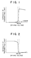
- a normally closed display mode where light is not transmitted when applying an OFF voltage and light is transmitted when applying an ON voltage, so that a larger pretilt angle is liable to increase leaked light in applying an OFF voltage and decrease the contrast of a displayed image, as shown in Fig. 1.
- Japanese Patent Publication Open to Public Inspection (hereinafter referred to as Japanese Patent 0.P.I. Publication) No. 63-274927/1988 discloses a technique for providing a single liquid crystal display device of a normally open display mode with an improved achromatic property by optimizing a value of ⁇ n ⁇ d and a setting angle of a polarizing plate. This technique, however, is liable to provide a darker display and a contrast not higher than 20 since ⁇ n ⁇ d is set at a small value.
- a transmission type liquid crystal display device comprising: a liquid crystal cell having a liquid crystal layer in which a nematic liquid crystal containing an optically active substance and having a positive dielectric anisotropy forms a twisted structure with a twist angle ⁇ ranging from 220° to 300° and is disposed between a pair of parallel electrode substrates each having a transparent substrate and provided thereon an electrode layer and an alignment layer so that the respective alignment layers contact the liquid crystal layer; a pair of front and rear polarizing plates each disposed on the side of the substrate opposite to the alignment layers; and a backlight source disposed on the side of the rear polarizing plate opposite to the substrate, wherein
- the angles ⁇ and ⁇ of the polarizing plates are in the specific range, so that the liquid crystal display device can have the normally open display mode where light is transmitted in applying an OFF voltage and no light is transmitted an ON voltage is applied, as shown in Fig. 2, and can provide a sufficiently high contrast.
- Such a high contrast is not lowered by leaked light even in a multiplex driving at a high duty ratio because that the pretilt angle ⁇ 0 is set at as large as not less than 10°.
- a high contrast and large capacity display can be provided in multiplex driving at a high duty ratio.
- ⁇ n ⁇ d and the angles ⁇ and ⁇ are in the specific ranges, respectively, and the luminous intensity ratios of red light in the backlight source are 1.2 or more, so that the displaying color of the liquid crystal display can give an excellent achromatic property applying an OFF voltage.
- the luminous intensity of the backlight source is not less than 200 cd/m2, so that tinting can be satisfactorily prevented without any adverse influence exerted by surrounding light incident in and reflected from the liquid crystal cell.
- a light-shielding layer may be provided on the non-picture element areas of an electrode substrate, which results in preventing light leakage from the non-picture element areas and further increasing the contrast of the whole display in a normally open display mode.
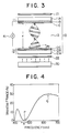
- the transmission type liquid crystal display device of the invention basically comprises:
- the display device is driven with a driving circuit 41.
- the nematic liquid crystal containing the optically active substance and having a positive dielectric anisotropy has the twist angle ⁇ in the range of 220° to 300°, and more preferably 250° to 270°.
- a transmitted light intensity is varied sharply in relation to a voltage variation. If the twist angle ⁇ is too small, the transmitted light intensity is varied slowly and the contrast is lowered. On the other hand, if it is too large, the alignment of the liquid crystal molecules becomes irregular when switching ON and OFF, so that the display quality is deteriorated.
- the twist angle ⁇ ranging from 250° to 270°, a light leakage in applying an ON voltage can be minimized and the highest contrast can be obtained.
- the twist angle ⁇ can be determined by the alignment directions of the alignment layers provided on the respective electrode substrates, and the kinds and quantities of the nematic liquid crystal and the optically active substances added thereto.
- the twist direction of the nematic liquid crystal may be either clockwise or counter-clockwise to the direction of incident light.
- the product ⁇ n ⁇ d in which ⁇ n is a refractive anisotropy of a nematic liquid crystal and d( ⁇ m) is a thickness of a liquid crystal layer, is 0.65 ⁇ 0.90 ⁇ m.
- ⁇ n ⁇ d in the above range contributes not only to effectively preventing tinting but also to sufficiently increasing the light transmittance in the whole wavelength region of visible light and provide a high contrast display.
- a conventional SBE type liquid crystal cell has a non-transmission spectral region A on the short wavelength side of the visible wavelength region of the transmission spectrum as shown in Fig. 4, in which almost no light can be transmitted.
- the non-trans-mission spectral region A is shifted to a shorter wavelength region by decreasing the value of ⁇ n ⁇ d.
- too small ⁇ n ⁇ d decreases the whole light transmittance in the visible wavelength region of 400 to 700 nm, so that the brightness in the light transmitting state becomes insufficient. Therefore, ⁇ n ⁇ d is preferably in the range of 0.65 to 0.90 ⁇ m.
- the optimum value of ⁇ n ⁇ d relates to an average tilt angle ⁇ OFF of a liquid crystal in applying an OFF voltage, and the more the average tilt angle ⁇ OFF is, the larger the optimum value of ⁇ n ⁇ d is.
- the results of experiments show that the excellent display characteristics can be obtained when ⁇ n ⁇ d and ⁇ OFF satisfy the following equation: ⁇ n ⁇ d ⁇ cos2 ⁇ OFF ⁇ 0.68 ⁇ 0.05 ⁇ m ⁇ n is a value of a reflective anisotropy of a nematic liquid crystal containing an optically active substance, and can be replaced with that of the liquid crystal containing no optically active substance since the content thereof is usually 5 weight%.
- the average tilt angle ⁇ OFF is an average value of the angle defined by the intersection of a director of liquid crystal molecules in applying an OFF voltage and an electrode substrate.
- the average tilt angle ⁇ OFF depends on the kind of the alignment layer, the pretilt angle, the physical properties of the nematic liquid crystal, and an applied voltage.
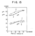
- Fig. 15 illustrates a relation between the average tilt angles and pretilt angles ⁇ 0 of liquid crystals ZLI-2293 made by Merck and CR-4008 made by chisso in applying an OFF voltage and an ON voltage in multiplex driving at a duty ratio of 1/100, wherein curves E and F correspond to ZLI-2293 and CR-4008, respectively.
- angles ⁇ and ⁇ set at the above range enables to display in a normally open display mode in which light leakage is lowered, and therefore to provide a color display with a higher color purity by combining the three color filters of red, green and blue.
- Equation (a) In combining a liquid crystal cell containing a nematic liquid crystal of a twisted structure with a pair of polarizing plates, and the angle ⁇ of one polarizing plate in the relation to the twist angle ⁇ of the liquid crystal layer can be determined by the above-given equation (a), which can minimize the transmittance in a non-light transmission state, provided that the distortion angle ⁇ of the other polarizing plate is fixed.
- Equation (a) light leakage in the non-light transmission state can be decreased by selecting the angles ⁇ and ⁇ in the relation to the twist angle ⁇ .
- the correction angle ⁇ depends on the average tilt angle ⁇ ON of the liquid crystal molecules in the non-light transmission state.
- the average tilt angle ⁇ ON getting closer to 90° makes the ⁇ value closer to 0°.
- the average tilt angle ⁇ ON is an average value of the angle defined by the intersection of the electrode substrate and the director of liquid crystal molecules in applying an ON voltage.
- the value of the left side of Equation (a) should be shifted to smaller value from 90° by the correction angle ⁇ according to the average tilt angle ⁇ ON in order to offset an optical activity caused by the retardation.
- the shifting direction has to be such that the value ⁇ is positive.
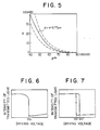
- Fig. 5 illustrates the correlation between the value ⁇ and the average tilt angle ⁇ ON in applying the ON voltage
- the solid line indicates the correlation between the average tilt angle ⁇ ON in applying the ON voltage and the value ⁇ , provided that ⁇ n ⁇ d is 0.77 ⁇ m
- the broken line indicates the range of the variation of ⁇ and ⁇ ON according to ⁇ n ⁇ d in the range of 0.65 to 0.90 ⁇ m.
- Fig. 15 illustrates the correlations between the average tilt angles ⁇ ON and the pretilt angles ⁇ 0 of the two kinds of liquid crystals, wherein it can be found that the larger the pretilt angle ⁇ 0 is, the larger the average tilt angle ⁇ ON is.
- the bistable phenomenon is defined by a phenomenon where, as shown in Fig. 6, there is observed a shift of a threshold voltage of a driving voltage when switching ON to OFF and OFF to ON.
- an intensity of transmitted light relative to a driving voltage changes sharply at the threshold voltage V th .
- the twist angle ⁇ has to be not less than 220°.
- too large twist angle ⁇ makes the bistable phenomenon too large and the transmitted light intensity relative to the driving voltage exhibits a hysteresis phenomenon.
- the response speed of the liquid crystal layer to the ON-to-OFF and OFF-to-ON switching of a driving voltage in multiplex driving becomes slow. Therefore, the twist angle ⁇ has to be not larger than 300° in order to increase the response speed.
- the brightness in the light transmission state can be maximized at the twist angle ⁇ of around 270° - ⁇ .
- the contrast can further be increased.
- the optimum value of the correction angle ⁇ in the above Equation (a) is determined depending on the types of the alignment layers and the physical properties of the liquid crystal.
- the liquid crystal cell having a larger ⁇ value has larger light leakage in the non-light transmission state, and the liquid crystal cell having a ⁇ value exceeding 30° can not provide any satisfactory contrast even if the other parameters are optimized.
- the pretilt angle ⁇ 0 is not smaller than 10°, the ⁇ value is in the range of 0° ⁇ ⁇ ⁇ 30°. The larger the bistable phenomenon of the liquid crystal cell is, the smaller the ⁇ value is.
- the optimum ⁇ value has to be determined for each combination.
- the optimum ⁇ value is determined in the following manner.
- Equation (a) the above ⁇ 0 corresponds to ⁇ /2, whereby the value ⁇ can be determined.
- the optimum values of the angles ⁇ and ⁇ can be determined according to Equations (a) and (b).
- the maximum contrast can be obtained at the optimum values and a satisfactorily high contrast can also be obtained in the vicinities of the above optimum values.
- the contrast changes remarkably when the angles ⁇ and ⁇ are deviated from the optimum values, and the angles ⁇ and ⁇ deviated by ⁇ 5° or more from the respective optimum values can provide no satisfactory contrast.
- the ON voltage is defined by an ON voltage V ON corresponding to an effective ON/OFF voltage ratio represented by: in multiplex driving at a 1/N duty ratio, and is an ON voltage where a response time t ON in switching from the light transmission state to the non-light transmission state of a display becomes equal to a response time t OFF in switching from the non-light transmission state to the light transmission state.
- the pretilt angle defined by the intersection of an electrode substrate and the director of liquid crystal molecules contacting the electrode substrate is not less than 10°, preferably not less than 25°.
- the pretilt angle ⁇ 0 not less than 10°.
- the pretilt angle ⁇ 0 not less than 10° can reduce the light leakage in the non-light transmission state to a sufficiently low level and make the contrast not lower than 30 practically in multiplex driving at a 1/100 duty ratio.
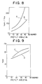
- Fig. 8 illustrates the actual relation between the pretilt angle ⁇ 0 and the contrast in multiplex driving at a 1/100 duty ratio, wherein curve A indicates the actual values in setting ⁇ n ⁇ d at 0.79 ⁇ m with a nematic liquid crystal ZLI-2293 manufactured by Merck, and curve B indicates the actual values in setting ⁇ n ⁇ d at 0.83 ⁇ m with a nematic liquid crystal CR-4008 manufactured by Chisso Co.
- the pretilt angle ⁇ 0 is not less than 10°, preferably not less than 25° in order to decrease the light leakage and in crease the contrast.
- Fig. 9 illustrates the actual relation between the pretilt angle ⁇ 0 and the brightness in multiplex driving at a 1/100 duty ratio, wherein curve C indicates the actual values in setting ⁇ n ⁇ d at 0.79 ⁇ m with the nematic liquid crystal ZLI-2293 manufactured by Merck, and curve D indicates the actual values in setting ⁇ n ⁇ d at 0.83 ⁇ m with the nematic liquid crystal CR-4008 manufactured by Chisso Co.
- the pretilt angle ⁇ 0 is not less than 10°, preferably not less than 25°.
- the backlight source has a red light luminous intensity of 1.2 times or more, preferably 1.5 to 2.5 times as much as those of the green and blue light.
- the emission spectrum of the backlight source adjusted as above to make the red light luminous intensity higher results in a satisfactorily flat spectrum of a transmission light through the liquid crystal cell and a display having an excellent achromatic property. It is hard to make the transmission spectrum completely flat only by adjusting the angles ⁇ and ⁇ .
- An ON-OFF contrast can be increased by a conventional backlight source, but a transmitted light is tinted with blue and, it is difficult to completely prevent tinting, because the transmittance of the red light wavelength region is low in the transmission spectrum of the liquid crystal cell in applying an OFF voltage, as shown in Fig. 10.
- red light, green light and blue light are defined by light having the wavelength regions of about 580 to 800 nm, about 480 to 580 nm and about 400 to 480 nm, respectively.
- the examples of the backlight sources applicable to the invention are a cold- cathode type fluorescent lamp, an incandescent cathode type fluorescent lamp, and an electroluminescent lamp.
- the cold-cathode type fluorescent lamp is particularly preferable from the viewpoints of luminous intensity, temperature and life.
- reference numeral 60 is a tubular light source
- 61 is a guide plate
- 62 is a reflecting plate
- 63 is a diffision plate.
- the higher luminous intensity of red light emitted from the backlight source can be achieved by making use of a light source capable of emitting high luminous intensity red light or by disposing filters on the backlight source so as to adjust the ratio of a red light luminous intensity to those of green and blue light.
- the backlight source has a luminous intensity of not less than 200 cd/m2 and, more preferably not less than 400 cd/m2.
- the backlight source having such high luminous intensity makes it possible to prevent an adverse effect caused by a surrounding light reflected from the front surface and reflected out of the liquid crystal cell, and provide a display having an excellent achromatic property.
- the luminous intensity of the backlight source is less than 200 cd/m2
- tinting as is observed in a reflection mode is caused by light reflected from both of the back surface of a liquid crystal cell and the front surface of a backlight source, which is incident from the front surface of the liquid crystal cell under an ordinary room light illumination, so that it is difficult to provide a display having an excellent achromatic property.
- the upper limit of the luminous intensity of the back-light source has no specific limit as far as heat of the back-light source adversely affects the liquid crystal.
- the backlight source of the higher luminance intensity consumes more electricity, and therefore it is preferable to increase the light transmittance of a liquid crystal cell including those of the polarizing plates to keep the necessary luminous intensity of the backlight source as low as possible.
- ⁇ n ⁇ d and the angles ⁇ and ⁇ of the polarizing plates are set in the specific ranges, respectively, so that the necessary luminous intensity of the backlight source can be kept lower because the light transmittance of the liquid crystal cell including those of the polarizing plates can be secured to be not lower than 20%.
- a polarization ratio of a polarizing plate is set at not less than 95% and, preferably not less than 99% for obtainining a higher contrast. If the polarization ratios of the polarizing plates are lower than the above, light leakage becomes larger in applying an ON voltage and a high contrast can not be provided even if the setting angles of the polarizing plates are optimized.
- the present invention satisfies preferably the following conditions:
- the nematic liquid crystal satisfying the above preferable conditions (1) to (3) can provide the bistable phenomenon only slightly and further accelerate the response speed of the liquid crystal layer to switching ON and OFF of a driving voltage in multiplex.
- a refractive anisotropy ⁇ n a splay elastic constant k11, a twist elastic constant k22, a bend elastic constant k33, a dielectric anisotropy ⁇ , a dielectric constant ⁇ , a transition temperature T NI , and a viscosity ⁇ are the physical properties of a nematic liquid crystal containing no optically active substance.
- a refractive anisotropy ⁇ n a splay elastic constant k11, a twist elastic constant k22, a bend elastic constant k33, a dielectric anisotropy ⁇ , a dielectric constant ⁇ , a transition temperature T NI , and a viscosity ⁇ are the physical properties of a nematic liquid crystal containing no optically active substance.
- the pretilt angle ⁇ 0 can be measured by a magneto-capacitive null method described in J. Appl. Phys., 48, 1783, (1977).
- the angle ⁇ is the setting angle of the polarizing plate on the incident light side
- the angle ⁇ is the setting angle of the polarizing plate on the outgoing light side.
- the setting angle is defined by the intersection of the projected direction of the director (a vector showing the average direction of the longitudinal axes of the liquid crystal molecules) of the liquid crystal molecules contacting an electrode substrate, and a polarizing axis (a transmittance axis or an absorption axis) of a polarizing plate disposed on the electrode substrate.
- the angles ⁇ and ⁇ of the polarizing plates are converted to the values ranging from -90° to +90° , for example, the angle ⁇ of 135° is converted to the angle ⁇ of -45°.
- the projected direction of the director of the liquid crystal milecules contacting the electrode substrate usually corresponds to the direction of an aligning treatment of an alignment layer on the electrode substrate.
- the direction of the aligning treatment corresponds to that of evaporation-deposition where the aligning treatment is performed in an oblique evaporation-deposition method, and to a rubbing direction where it is performed in a rubbing method.
- the polarizing axes of the polarizing plates may be either a transmittance axis or an absorption axis. Where both of the angles ⁇ and ⁇ depend either on the transmittance axes or the absorption axes, the display device can have a normally open display mode in which a light transmission state is in applying an OFF voltage and a non-light transmission state in applying an ON voltage.
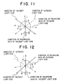
- the signs of the angles ⁇ and ⁇ are defined in the following manner. As shown in Fig. 11, where a twist direction of liquid crystal molecules is counterclockwise along a propagating direction of incident light, a positive sign is assigned to a clockwise direction toward the direction of a polarizing axis from the director of liquid crystal molecules in contact with an electrode substrate. Meanwhile, as shown in Fig. 12, where a twist direction of liquid crystal molecules is clockwise along the propagating direction of incident light, a positive sign is assigned to a counterclockwise direction.
- the spontaneous twist pitch P S is defined by a pitch in an intrinsic twist configuration of a liquid crystal layer, which is formed by adding an optically active substance to a nematic liquid crystal.
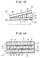
- the spontaneous twist pitch P S can be determined in accordance with the following equation given below and in the following manner: As shown in Fig. 13, a liquid crystal cell 55 is formed by arranging wedgewise the electrode substrates 53, 54 having the alignment layers 51, 52 so that the alignment layers are oppositely disposed.
- 57 is a spacer
- 58, 59 are the polarizing plates.
- Alignment layers 51, 52 are aligned so that the direction of aligning treatment are parallel to each other.
- k33/k22 and k33/k11 can be determined by the method where the values thereof are determined by a threshold value of an electrical capacity variation or a threshold value of an optical variation observed in applying a magnetic field to a uniformly aligned liquid crystal cell, described in H. Gluler et al, Z. Naturforsch, 279, (1972), 966; another method where they are determined by a variation of an electrical capacity observed in applying an electric field to a uniformly aligned liquid crystal cell, described in H. Deuling, Mol. Cryst. Liq. Cryst. 19, (1972) 123.
- a brightness is herein evaluated in terms of the level of the transmittance represented by luminance value Y, and a contrast value is evaluated in terms of a Y OFF /Y ON ratio in which Y OFF and Y ON represent the luminance values in applying an OFF and ON voltage, respectively.
- the materials for the transparent substrates 11A and 12A are glass such as soda glass, borosilicate glass and quartz glass; and plastic sheets made of uniaxial oriented polyethylene terephthalate, polyether sulfone and polyvinyl alcohol.
- the electrode layers 11B and 12B are composed of the transparent electrodes having ITO (oxide of tin and indium) and tin oxide each provided on the surfaces of the transparent substrates 11A and 12A.
- the alignment layers 11C and 12C can be provided by the conventional methods. In the invention, the following methods are particularly preferable because it requires to set the pretilt angle ⁇ 0 at 10° or more:
- a light-shielding layer on the non-picture element regions of an electrode substrate, which can prevent light leakage from the non-picture element regions, so that the non-picture element regions can be darkened more and the contrast can be further increased.
- the light-shielding layer is composed of a metal layer such as chromium and nickel, a layer containing black silver dispersed in an insulating binder such as gelatin, or a layer containing a dye or pigment dispersed in an insulating binder.
- the upper and lower electrode substrates 11 and 12 may be provided with an insulating layer, a dielectric layer, an alkali-ion migration preventive layer, an antireflection layer, and a polarizing layer.
- the color filters can be formed preferably by coating an emulsion layer containing a silver halide dispersed in an insulating biner such as gelatin and developing the emulsion layer by a silver salt photographic process.
- the color filters may be formed by a dyeing process, a printing process, or an electrodeposition process.
- nematic liquid crystals Various kinds of the nematic liquid crystals can be used.
- the nematic liquid crystals applicable to the invention may contain smectic and cholesteric liquid crystals.
- nematic liquid crystal As for the optically active substance which may be added to the nematic liquid crystal, a so-called chiral nematic liquid crystal is generally used, which is an ester, biphenyl, phenylcyclohexane or azo type nematic liquid crystal having an optically active group represented by the following formula as a terminal group: wherein R1, R2 and R3 each represent an alkyl group and a hydrogen atom and are different from each other.
- the optically active substances applicable to the invention are preferably those capable of shortening a spontaneous twist pitch per unit amount added to the nematic liquid crystal.
- Such optically active substances can control an addition amount thereof to a lower level, preferably not more than 2.0% by weight.
- a lower level preferably not more than 2.0% by weight.
- T NI transition temperature
- the optically active substances there may be used in combination some kinds of the optically active substances having the reverse signs of the temperature variation coefficient of the spontaneous twist pitch.
- Fig. 14 is a schematic illustration of a liquid crystal cell 10, wherein the upper electrode substrate 11 and the lower electrode substrate 12 are disposed oppositely via a space.
- the electrode substrates comprise the electrode layers 11B, 12B and the alignment layers 11C, 12C provided on the transparent substrates 11A, 12A so that the respective electrode layers and alignment layers are opposite each other via the space.
- a light-shielding layer 12D is provided on a non-picture element area.
- the space between the electrode substrates is sealed with a sealing member 15 to constitute the liquid crystal cell 10.
- a sealing member 15 there are disposed in the liquid crystal cell 10 a plurality of spacers 16 separately, and a nematic liquid crystal containing an optically active substance and having a positive dielectric anisotropy, in which there is formed the twisted structure with a twist angle ranging from 220° to 300°, whereby a liquid crystal layer 13 is formed.
- the front and rear polarizing plates 21 and 22 are disposed on the outside surfaces of the electrode substrates, respectively.
- the transpatrent substrates 11A and 12A are composed of the soda glasses of which surface is polished to a flatness of not more than 0.1 ⁇ m and then is provided with an alkali-ion migration prevention layer of SiO2.
- the electrode layers 11B and 12B are composed of the transparent electrodes comprising an ITO layer provided on the transparent substrates and having a thickness of 1500 ⁇ .
- a transparent electrode constituting the electrode layer 11B was arranged in the direction perpendicular to that of the other electrode layer 12B, whereby an electrode structure of a matrix display is formed.
- the light-shielding layer 12D is composed of a gelatin layer in which black silver is dispersed.
- the backlight source illustrated in Fig. 16(A), in which a cold-cathode fluorescent lamp is combined with a guide plate, is provided on the backside of the rear polarizing plate 22.
- liquid crystal cells having the structure shown in Fig. 14 were prepared in the conditions shown in Tables 1 and 2 given below and used for manufacturing the transmission type liquid crystal display device shown in Fig. 3.
- the front and rear polarizing plates 21 and 22 were made of NPF-G1220DU manufactured by Nitto Electric Works Co.
- the spacer 16 was made of glass fiber and the sealing member 15 was made of Structbond XN-5A-C manufactured by Mitsui Toatu Chemicals, Inc.
- Each of the transmission type liquid crystal display devices were tested for displaying in multiplex driving at a 1/100 duty ratio and evaluated for a contrast, an achromatic property and a brightness.
- the achromatic property was evaluated by observing visually a displayed image.
- the results of the evaluation were ranked at ' ⁇ ' as almost no tinting and a clear display; ' ⁇ ' as slight tinting with no problem for practical use; and ' ⁇ ' as serious tinting and inferior display.
- the transmission type liquid crystal display devices of the invention can provide an excellent display having a high contrast and a superior achromatic property.
- the comparative transmission type liquid crystal display devices have the inferior contrast, achromatic property and brightness.
- Comparison 1 has an inferior brightness to Example 1 because of ⁇ n ⁇ d less than 0.65.
- Comparison 2 The achromatic property of Comparison 2 is less improved than that of Example 1 because of ⁇ n ⁇ d more than 0.90, even though the luminous intensity of the backlight source is controlled.
- Example 3 the pretilt angles are smaller than in Example 1.
- the contrast has been able to reach the level of more than 30 because of the pretilt angle not less than 10°.
- the values of ⁇ n ⁇ d are optimized by reducing them according to decreasing of the pretilt angle.
- Comparison 3 has much inferior contrast than Example 2 due to the ⁇ value larger than 30, which is attributable to the pretilt angle smaller than 10°, even though the setting angles of the polarizing plates are optimized.
- Comparison 4 has the worse contrast and bightness than Examples because of the pretilt angle smaller than 10° and ⁇ n ⁇ d smaller than 0.65, even though the bistability is increased by making (Pc - Psd)/Ps negative.
- Example 6 has the inferior achromatic property because of the lower luminous intensity of the backlight source than Example 1, but the tinting is within an allowable level because of the luminous intensity of not less than 200 cd/m2.
- Comparison 5 has the inferior achromatic property due to blue tinting which is attributable to the luminous intensity of the backlight source not more than 200 cd/m2
- Example 7 The achromatic property of Example 7 is not so good as those of other Examples because the luminous intensity ratios of red light to green light and blue light are smaller than those of other Examples, but within an allowable limit because of the ratios larger than 1.2. In Comparison 6, the achromatic property is inferior because of the luminous intensity ratios less than 1.2.
Landscapes
- Physics & Mathematics (AREA)
- Nonlinear Science (AREA)
- Chemical & Material Sciences (AREA)
- Crystallography & Structural Chemistry (AREA)
- General Physics & Mathematics (AREA)
- Optics & Photonics (AREA)
- Liquid Crystal (AREA)
Applications Claiming Priority (2)
| Application Number | Priority Date | Filing Date | Title |
|---|---|---|---|
| JP1092926A JP2784205B2 (ja) | 1989-04-14 | 1989-04-14 | 透過型液晶表示装置 |
| JP92926/89 | 1989-04-14 |
Publications (3)
| Publication Number | Publication Date |
|---|---|
| EP0392811A2 true EP0392811A2 (de) | 1990-10-17 |
| EP0392811A3 EP0392811A3 (en) | 1990-12-19 |
| EP0392811B1 EP0392811B1 (de) | 1993-12-29 |
Family
ID=14068097
Family Applications (1)
| Application Number | Title | Priority Date | Filing Date |
|---|---|---|---|
| EP90303872A Expired - Lifetime EP0392811B1 (de) | 1989-04-14 | 1990-04-10 | Transmissive Flüssigkristall-Anzeigevorrichtung |
Country Status (4)
| Country | Link |
|---|---|
| US (1) | US5048933A (de) |
| EP (1) | EP0392811B1 (de) |
| JP (1) | JP2784205B2 (de) |
| DE (1) | DE69005505D1 (de) |
Cited By (4)
| Publication number | Priority date | Publication date | Assignee | Title |
|---|---|---|---|---|
| NL9401983A (nl) * | 1993-11-26 | 1995-06-16 | Nokia Technology Gmbh | Vloeibaar-kristalafbeeldinrichting. |
| EP0992836A3 (de) * | 1994-12-09 | 2000-08-09 | Seiko Instruments Inc. | Anzeigevorrichtung und Methode zu ihrer Herstellung |
| EP1251370A4 (de) * | 2000-01-27 | 2003-09-03 | Fuji Photo Film Co Ltd | Folienpolarisator mit vielzahl von lichtstreuenden und lichtabsorbierenden elementen |
| EP1033606A3 (de) * | 1999-02-25 | 2004-01-28 | Hitachi, Ltd. | Flüssigkristallanzeigevorichtung |
Families Citing this family (17)
| Publication number | Priority date | Publication date | Assignee | Title |
|---|---|---|---|---|
| US5377028A (en) * | 1990-10-01 | 1994-12-27 | Casio Computer Co., Ltd. | Liquid crystal display device with liquid crystal elastic constant ratio at least 1.75 |
| JPH04294323A (ja) * | 1991-03-25 | 1992-10-19 | Hitachi Ltd | 液晶表示装置 |
| TW255017B (de) * | 1991-12-26 | 1995-08-21 | Toshiba Co Ltd | |
| DE4212744C2 (de) * | 1992-04-16 | 1994-10-13 | Merck Patent Gmbh | TN-Zelle mit d. DELTAn zwischen 0,15 und 0,70 mum |
| JP2933261B2 (ja) * | 1993-12-27 | 1999-08-09 | シャープ株式会社 | 液晶表示装置 |
| US5699133A (en) * | 1995-05-30 | 1997-12-16 | Sanyo Electric Co., Ltd. | Liquid crystal shutter having a specified zero voltage time viscosity product or a specified driving frequency |
| EP0793814B1 (de) * | 1995-09-25 | 2005-06-15 | Koninklijke Philips Electronics N.V. | Elektrolumineszentes beleuchtungssystem und flachtafelbildanzeigevorrichtung mit einem solchen system |
| KR100405893B1 (ko) * | 1995-10-23 | 2004-10-06 | 가부시끼가이샤 히다치 세이사꾸쇼 | 액정표시장치 |
| US6137456A (en) * | 1996-07-01 | 2000-10-24 | Corning Incorporated | Electronic display device for simultaneously displaying 2D and 3D images |
| JP3814774B2 (ja) * | 1999-02-08 | 2006-08-30 | 日東電工株式会社 | 偏光部材、光学部材及び液晶表示装置 |
| KR100784804B1 (ko) * | 2001-05-07 | 2007-12-14 | 삼성전자주식회사 | 액정 표시 장치 및 제조 방법 |
| US20060154396A1 (en) * | 2001-08-15 | 2006-07-13 | Nitto Denko Corporation | Polarizing element and optical member and liquid crystal display device |
| US6919946B2 (en) * | 2002-04-16 | 2005-07-19 | 3M Innovative Properties Company | Compensators for liquid crystal displays and the use and manufacture of the compensators |
| JP4027164B2 (ja) * | 2002-06-21 | 2007-12-26 | 株式会社日立製作所 | 表示装置 |
| JP2004342336A (ja) | 2003-05-13 | 2004-12-02 | Semiconductor Energy Lab Co Ltd | 発光装置およびその作製方法 |
| US7192326B2 (en) * | 2003-08-29 | 2007-03-20 | Semiconductor Energy Laboratory Co., Ltd. | Method of manufacturing a light-emitting element using a rubbing treatment |
| CN100483205C (zh) * | 2004-02-06 | 2009-04-29 | 富士胶片株式会社 | 显示装置用遮光膜、其制作方法、含金属微粒的组合物 |
Family Cites Families (14)
| Publication number | Priority date | Publication date | Assignee | Title |
|---|---|---|---|---|
| JPS5923328A (ja) * | 1982-07-29 | 1984-02-06 | Sharp Corp | 液晶表示装置 |
| IN161652B (de) * | 1983-07-12 | 1988-01-09 | Bbc Brown Boveri & Cie | |
| DE3433248A1 (de) * | 1984-09-11 | 1986-03-20 | Merck Patent Gmbh, 6100 Darmstadt | Elektrooptisches anzeigeelement |
| JPS61210324A (ja) * | 1985-03-15 | 1986-09-18 | Hitachi Ltd | 液晶表示素子 |
| JPS6231822A (ja) * | 1985-08-02 | 1987-02-10 | Hitachi Ltd | 液晶表示素子 |
| DE3609141A1 (de) * | 1986-03-19 | 1987-09-24 | Merck Patent Gmbh | Elektrooptisches anzeigeelement |
| JPS62231218A (ja) * | 1986-03-31 | 1987-10-09 | Matsushita Electric Ind Co Ltd | マトリクス型液晶表示装置 |
| JPS6348522A (ja) * | 1986-08-19 | 1988-03-01 | Matsushita Electric Ind Co Ltd | マトリクス型液晶表示装置 |
| JP2676508B2 (ja) * | 1986-09-12 | 1997-11-17 | コニカ株式会社 | 液晶表示装置 |
| JP2575445B2 (ja) * | 1987-02-16 | 1997-01-22 | 株式会社東芝 | 液晶表示器 |
| JPS63274926A (ja) * | 1987-05-07 | 1988-11-11 | Asahi Glass Co Ltd | 液晶表示素子 |
| JPS63274924A (ja) * | 1987-05-07 | 1988-11-11 | Asahi Glass Co Ltd | 液晶表示素子 |
| JPS6431119A (en) * | 1987-07-27 | 1989-02-01 | Sharp Kk | Color liquid crystal display device |
| JP2674600B2 (ja) * | 1988-05-07 | 1997-11-12 | コニカ株式会社 | 液晶表示装置 |
-
1989
- 1989-04-14 JP JP1092926A patent/JP2784205B2/ja not_active Expired - Lifetime
-
1990
- 1990-04-10 US US07/506,802 patent/US5048933A/en not_active Expired - Lifetime
- 1990-04-10 DE DE90303872T patent/DE69005505D1/de not_active Expired - Lifetime
- 1990-04-10 EP EP90303872A patent/EP0392811B1/de not_active Expired - Lifetime
Cited By (5)
| Publication number | Priority date | Publication date | Assignee | Title |
|---|---|---|---|---|
| NL9401983A (nl) * | 1993-11-26 | 1995-06-16 | Nokia Technology Gmbh | Vloeibaar-kristalafbeeldinrichting. |
| EP0992836A3 (de) * | 1994-12-09 | 2000-08-09 | Seiko Instruments Inc. | Anzeigevorrichtung und Methode zu ihrer Herstellung |
| EP1033606A3 (de) * | 1999-02-25 | 2004-01-28 | Hitachi, Ltd. | Flüssigkristallanzeigevorichtung |
| KR100745115B1 (ko) * | 1999-02-25 | 2007-08-01 | 가부시끼가이샤 히다치 세이사꾸쇼 | 액정표시장치 |
| EP1251370A4 (de) * | 2000-01-27 | 2003-09-03 | Fuji Photo Film Co Ltd | Folienpolarisator mit vielzahl von lichtstreuenden und lichtabsorbierenden elementen |
Also Published As
| Publication number | Publication date |
|---|---|
| JPH02272519A (ja) | 1990-11-07 |
| DE69005505D1 (de) | 1994-02-10 |
| US5048933A (en) | 1991-09-17 |
| JP2784205B2 (ja) | 1998-08-06 |
| EP0392811A3 (en) | 1990-12-19 |
| EP0392811B1 (de) | 1993-12-29 |
Similar Documents
| Publication | Publication Date | Title |
|---|---|---|
| EP0392811B1 (de) | Transmissive Flüssigkristall-Anzeigevorrichtung | |
| US5847789A (en) | Reflective type liquid crystal display device | |
| JP3339334B2 (ja) | 反射型液晶表示素子 | |
| EP1331509B1 (de) | Transflektierende Flüssigkristallanzeige | |
| EP0780721B1 (de) | Flüssigkristall-Anzeigevorrichtung vom Reflexionstyp | |
| JPH09160042A (ja) | 液晶表示素子 | |
| EP0259822B2 (de) | Flüssigkristall-Anzeigevorrichtung | |
| US6144432A (en) | Reflective liquid crystal display device | |
| US20020180914A1 (en) | Reverse transmittance mode direct-view liquid crystal display employing a liquid crystal having a characteristic wavelength in the non-visible spectrum | |
| JPH1096887A (ja) | カラー液晶表示素子 | |
| US4974940A (en) | Liquid crystal display device | |
| EP0341702B1 (de) | Flüssigkristall-Anzeigevorrichtung | |
| US6072553A (en) | Reflection-type liquid crystal display with layer comprising liquid crystal compound and liquid crystal polymer being twist-aligned at same angle | |
| KR100306648B1 (ko) | 반사형 액정표시 소자 | |
| JP2673536B2 (ja) | 液晶表示装置 | |
| US6633352B2 (en) | Reflection type liquid crystal display device | |
| KR100303715B1 (ko) | 액정 표시 장치 | |
| EP0352792A2 (de) | Flüssigkristallvorrichtung | |
| JP3580994B2 (ja) | 液晶表示装置 | |
| JP2567820B2 (ja) | 液晶表示装置 | |
| Ohgawara et al. | Development of a multicolour super-twisted-nematic display | |
| JPS62127714A (ja) | 液晶表示装置 | |
| JP2947801B2 (ja) | ねじれらせん構造を有するネマチツク液晶表示装置 | |
| JPH0785142B2 (ja) | 液晶表示装置 | |
| JPH0862568A (ja) | 液晶表示装置 |
Legal Events
| Date | Code | Title | Description |
|---|---|---|---|
| PUAI | Public reference made under article 153(3) epc to a published international application that has entered the european phase |
Free format text: ORIGINAL CODE: 0009012 |
|
| AK | Designated contracting states |
Kind code of ref document: A2 Designated state(s): DE FR GB |
|
| PUAL | Search report despatched |
Free format text: ORIGINAL CODE: 0009013 |
|
| AK | Designated contracting states |
Kind code of ref document: A3 Designated state(s): DE FR GB |
|
| 17P | Request for examination filed |
Effective date: 19910525 |
|
| 17Q | First examination report despatched |
Effective date: 19930324 |
|
| GRAA | (expected) grant |
Free format text: ORIGINAL CODE: 0009210 |
|
| AK | Designated contracting states |
Kind code of ref document: B1 Designated state(s): DE FR GB |
|
| PG25 | Lapsed in a contracting state [announced via postgrant information from national office to epo] |
Ref country code: FR Effective date: 19931229 Ref country code: DE Effective date: 19931229 |
|
| REF | Corresponds to: |
Ref document number: 69005505 Country of ref document: DE Date of ref document: 19940210 |
|
| PG25 | Lapsed in a contracting state [announced via postgrant information from national office to epo] |
Ref country code: GB Effective date: 19940410 |
|
| EN | Fr: translation not filed | ||
| PLBE | No opposition filed within time limit |
Free format text: ORIGINAL CODE: 0009261 |
|
| STAA | Information on the status of an ep patent application or granted ep patent |
Free format text: STATUS: NO OPPOSITION FILED WITHIN TIME LIMIT |
|
| GBPC | Gb: european patent ceased through non-payment of renewal fee |
Effective date: 19940410 |
|
| 26N | No opposition filed |