EP0393997A2 - Procédé pour fabriquer un boîtier à cadre de connection dont les contacts sont à pas variable - Google Patents
Procédé pour fabriquer un boîtier à cadre de connection dont les contacts sont à pas variable Download PDFInfo
- Publication number
- EP0393997A2 EP0393997A2 EP90304121A EP90304121A EP0393997A2 EP 0393997 A2 EP0393997 A2 EP 0393997A2 EP 90304121 A EP90304121 A EP 90304121A EP 90304121 A EP90304121 A EP 90304121A EP 0393997 A2 EP0393997 A2 EP 0393997A2
- Authority
- EP
- European Patent Office
- Prior art keywords
- section
- conductive elements
- bump
- pitch
- leadframe
- Prior art date
- Legal status (The legal status is an assumption and is not a legal conclusion. Google has not performed a legal analysis and makes no representation as to the accuracy of the status listed.)
- Granted
Links
Images



Classifications
-
- H—ELECTRICITY
- H10—SEMICONDUCTOR DEVICES; ELECTRIC SOLID-STATE DEVICES NOT OTHERWISE PROVIDED FOR
- H10W—GENERIC PACKAGES, INTERCONNECTIONS, CONNECTORS OR OTHER CONSTRUCTIONAL DETAILS OF DEVICES COVERED BY CLASS H10
- H10W72/00—Interconnections or connectors in packages
- H10W72/701—Tape-automated bond [TAB] connectors
-
- H—ELECTRICITY
- H05—ELECTRIC TECHNIQUES NOT OTHERWISE PROVIDED FOR
- H05K—PRINTED CIRCUITS; CASINGS OR CONSTRUCTIONAL DETAILS OF ELECTRIC APPARATUS; MANUFACTURE OF ASSEMBLAGES OF ELECTRICAL COMPONENTS
- H05K3/00—Apparatus or processes for manufacturing printed circuits
- H05K3/30—Assembling printed circuits with electric components, e.g. with resistors
- H05K3/32—Assembling printed circuits with electric components, e.g. with resistors electrically connecting electric components or wires to printed circuits
- H05K3/34—Assembling printed circuits with electric components, e.g. with resistors electrically connecting electric components or wires to printed circuits by soldering
- H05K3/341—Surface mounted components
- H05K3/3421—Leaded components
- H05K3/3426—Leaded components characterised by the leads
-
- H—ELECTRICITY
- H10—SEMICONDUCTOR DEVICES; ELECTRIC SOLID-STATE DEVICES NOT OTHERWISE PROVIDED FOR
- H10W—GENERIC PACKAGES, INTERCONNECTIONS, CONNECTORS OR OTHER CONSTRUCTIONAL DETAILS OF DEVICES COVERED BY CLASS H10
- H10W70/00—Package substrates; Interposers; Redistribution layers [RDL]
- H10W70/40—Leadframes
- H10W70/421—Shapes or dispositions
-
- H—ELECTRICITY
- H10—SEMICONDUCTOR DEVICES; ELECTRIC SOLID-STATE DEVICES NOT OTHERWISE PROVIDED FOR
- H10W—GENERIC PACKAGES, INTERCONNECTIONS, CONNECTORS OR OTHER CONSTRUCTIONAL DETAILS OF DEVICES COVERED BY CLASS H10
- H10W72/00—Interconnections or connectors in packages
- H10W72/071—Connecting or disconnecting
- H10W72/077—Connecting of TAB connectors
-
- H—ELECTRICITY
- H05—ELECTRIC TECHNIQUES NOT OTHERWISE PROVIDED FOR
- H05K—PRINTED CIRCUITS; CASINGS OR CONSTRUCTIONAL DETAILS OF ELECTRIC APPARATUS; MANUFACTURE OF ASSEMBLAGES OF ELECTRICAL COMPONENTS
- H05K3/00—Apparatus or processes for manufacturing printed circuits
- H05K3/30—Assembling printed circuits with electric components, e.g. with resistors
- H05K3/32—Assembling printed circuits with electric components, e.g. with resistors electrically connecting electric components or wires to printed circuits
- H05K3/34—Assembling printed circuits with electric components, e.g. with resistors electrically connecting electric components or wires to printed circuits by soldering
- H05K3/341—Surface mounted components
- H05K3/3421—Leaded components
-
- Y—GENERAL TAGGING OF NEW TECHNOLOGICAL DEVELOPMENTS; GENERAL TAGGING OF CROSS-SECTIONAL TECHNOLOGIES SPANNING OVER SEVERAL SECTIONS OF THE IPC; TECHNICAL SUBJECTS COVERED BY FORMER USPC CROSS-REFERENCE ART COLLECTIONS [XRACs] AND DIGESTS
- Y02—TECHNOLOGIES OR APPLICATIONS FOR MITIGATION OR ADAPTATION AGAINST CLIMATE CHANGE
- Y02P—CLIMATE CHANGE MITIGATION TECHNOLOGIES IN THE PRODUCTION OR PROCESSING OF GOODS
- Y02P70/00—Climate change mitigation technologies in the production process for final industrial or consumer products
- Y02P70/50—Manufacturing or production processes characterised by the final manufactured product
Definitions
- the present invention relates to the field of electronic component manufacturing and packaging.
- a problem in the prior art of electronic component packaging includes inefficient steps in the production of leadframes for bonding with variably sized and pitched component packages.
- the substantial inefficiencies inherent in requiring different leadframes to be manufactured for connecting different packages to printed circuit boards is both costly and wasteful.
- cost and material savings combine to greatly improve the manufacturing and packaging processes.
- the present package to board variable pitch tab leadframe invention overcomes the problems identified above.
- the present invention is a variable pitch tab leadframe assembly.
- the leadframe assembly comprises a plurality of patterned conductive elements for transmitting input and output signals to bonding locations on an electronic device.
- the leadframe assembly comprises conductive elements with a variable pitch to accommodate a plurality of standard pitch bond site printed circuit board footprints.
- inventions described in the present application relate to improvements in manufacturing, bonding, and packaging of electronic components to achieve improved reliability, improved yield, and greater material and manufacturing efficiencies.
- the improvements comprise unique features including etched shadow mask construction, conductive metalized bump composition, and preferred structure of tape leadframes.
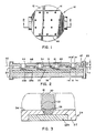
- mask 10 is illustrated. It is appreciated that masks, also known as shadow masks or vapor deposition masks, are variously constructed and shaped; however, the basic function of masks is to provide vapor deposition patterns for conductive material to be evaporated onto a die thereunder. Accordingly, mask 10 comprises a mask top surface 12 which defines apertures or vias 16. Mask 10 is removably mounted on a surface of a die and positioned in a chamber in which evaporation and deposition of solderable material will occur. During the evaporation and deposition process, the solderable material passes through vias 16 in mask 10 and is deposited in a pattern on the die. This provides a pattern of solderable material on the die for later reflowing, bonding, or other operations.
- Figure 2 is a side elevation cross section view taken generally along lines 2-2 of Figure 1 showing mask 10 removably mounted onto die 24 by mounting means 20.
- Die 24 may comprise a semiconductor chip, or a wafer comprising numerous semiconductor chips. Die 24 may comprise various materials and layers, however, a representative material combination in the die upper passivation region 25 includes a passivation portion 25a, such as silicon nitride, or more generally an insulator material, and a metalized portion 25b, such as aluminum, or more generally a conductive metalization.
- metalized portions 25b comprise conductive interconnects and are, therefore, deposition sites for later depositing of the vaporized solderable material. More specifically, interface metalization 28, shown in Figure 3, is commonly deposited first onto metalized portion 25b, and then solderable bump material 30, also shown in Figure 3, is then vapor deposited through vias 16 onto interface metalization 28.
- Figure 2 shows die 24 comprising top surface 34 and bottom surface 36.
- Figures 2 and 3 therefore illustrate die 24 having a plurality of deposit sites etched or otherwise positioned to provide solderable material in the form of bumps onto interface metalization 28, and extending generally from die top surface 34.
- a mask of suitable rigidity and via pattern must be used.
- Such masks are frequently made of metallic materials, as preferably is mask 10, which is typically constructed of molybdenum; however, other materials may be utilized such as glass or plastic.
- Mask 10 comprises mask top surface 12 which functions as an outer surface facing away from die 24 in operation, and which is located opposite mask bottom surface 13.
- vias 16 extend through mask 10 between top surface 12 and bottom surface 13 to permit vaporized bonding metals to pass through the mask and to deposit onto predetermined locations of die 24.
- mask bottom surface 13 comprises a plurality of recessed regions 44. Regions 44 are constructed to minimize the area of mask 10 in contact with die 24 during the vapor deposition process.
- the arrangement of recessed regions 44 in relation to bottom surface 13 surrounding vias 16 provides for substantially full mask thickness via regions having a width labelled R which provide damming action about the via to retain the vapor deposit within the predetermined deposit sites of die 24 defined by the via regions.
- recessed regions 44 are constructed and arranged for placement at a distance D from die surface 34.
- mask 10 bottom surface 13 includes etched recessed regions 44 which define a projection 49 located around each via 16. Projections 49 extend from the plane or planes 50 which includes base surfaces 47 of etched recessed regions 44 to minimize the contact area of mask 10, to only that area of bottom surface 13, in contact with die 24 during the entire process of vapor deposition.
- reinforcing ridges 66 may be utilized for stiffening mask 10. Reinforcing ridges 66 may be arranged in various orientations and shapes to achieve the advantages within the scope of this invention. Indeed, reinforcing ridges 66 need not be limited to protrusions from top surface 12 but instead may comprise material which is hardened in relation to the mask material comprising the remainder of mask 10.
- mask 10 comprises a molybdenum mask having a full thickness of 4 mils.
- Preferred mask 10 may be used with a die having passivation and metalization combined thickness of approximately 20 mils. Moreover, such a combination would provide means for depositing about a .5 micron thin film interface metalization 28, and a subsequent 100 micron thickness solderable material 30, as shown generally and not to scale in Figure 3. It is appreciated that sizes and shapes shown herein may vary considerably with each production requirement. The substantial reduction of contact surface area between mask 10 and die 24 is most relevant, as is the manner in which mask 10 prevents unwanted deposition of conductive metalization onto areas of die 24 beyond the via areas labelled by diameter R′.
- a method of manufacturing a damage reducing etched shadow mask 10 for providing vapor deposition patterns of bonding metals onto a surface of die 24 is also provided.
- This method preferably comprises the steps of providing a nonwettable shadow mask 10 having top surface 12 and bottom surface 13; creating vias 16 extending through mask 10; and etching portions of mask 10 bottom surface 13 to provide recessed regions 44 and substantially full thickness regions (having height labelled E and width comprising the thickness of R-R′ as shown in Figure 2), the recessed regions 44 providing for a reduced surface area in contact with die 24 during a vapor deposition process.
- the etching step may further comprise providing projections 49 or ridges extending annularly from vias 16 at bottom surface 13 of mask 10.
- Mask 10 permits manufacture and deposition through evaporation of a plurality of bumps comprising solderable conductive bump material 30, Figure 3, and which is shown in shadow 31 in a reflowed configuration.
- FIG. 4a An example of non-uniform conductive bump heights is shown in Figure 4a in which prior art gold bumps 61a, 61b, 61c, and 61d are arranged on die 62. As illustrated, bumps 61a, 61b, 61c, and 61d have different heights representative of the non-uniformity of bump heights often present in such structures.
- a representative leadframe assembly is positioned over die 62 and the bumps, with the leadframe assembly comprising conductive metal leads 63.
- Figure 4b illustrates the structures of Figure 4a after a planar bonding force has been applied to leads 63 by bonding tip means 66.
- the bonding force has caused die 62 to fracture below gold bump 61b due to the high bump height of that bump.
- leads 63 have contacted and bonded with correspondingly located bumps 61b and 61d.
- gold bump 61c has not bonded with its lead due to the short bump height of bump 61c. This results in non-conductivity and improper performance of a device using die 62 and relying on a bond between bump 61c and its lead.
- Figure 5a and 5b are cross section elevation views of a leadframe with organic standoff means arranged for bonding with solder bumps.
- Height standoff means 64 is commonly provided to prevent overcompression of leads 63 into the conductive bonding material of relatively soft bumps such as solder bumps 61e which do not maintain a uniform standoff height when bonding tip means 66 is brought into contact with leads 63 to form a connection between leads 63 and die 62 via the solder bump 61e.
- Height standoff means 64, or dielectric means is frequently constructed of organic material which is subject to moisture collection and long term deterioration.
- the present tin cap on solid base bump invention solves the problems illustrated in Figures 4b and 5b.
- cracking of die 62 under prior art gold bumps such as 61b is substantially reduced when such prior art gold bumps are replaced by the present tin cap on solid base bump invention.
- open connections such as shown above prior art gold bump 61c in Figure 4b are substantially reduced when such prior art gold bumps are replaced by the present tin cap on solid base bump invention.
- height standoff means 64 comprising organic material can be eliminated, thus creating the option of a package free of organic material, consistent with requirements such as those of U.S. Department of Defense Military Standard 38510.
- conductive lead 84 such as a portion of a conductive metalized leadframe
- a schematic conductive metalized bump 98 is also shown positioned on a die 90.
- Bump 98 preferably comprises a bump lower portion 92 comprising a gold base material of substantially 100% by weight gold to provide a substantially fixed standoff height during the bonding process.
- Bump 98 preferably also comprises a bump upper portion 94 comprising an effective amount of tin deposited on a top surface 97 of the gold base material comprising the bump lower portion 92.
- Preferred tin cap on gold base bump 98 provides improved means for interconnecting electronic components and comprises improved fatigue and expansion coefficient properties over solder bumps on dies. This gold-tin combination bond provides a high strength reflowable alloy.
- a suitable base material may be comprised of at least one metal selected from a group consisting of chrome, nickel, titanium-tungsten, cobalt, and copper.
- a tin cap on a solid base bump may be employed without using only a gold base.
- a solid base of nickel or other suitable conductive material is within the scope of this invention.
- a bump comprising a tin cap upper portion 94 on a solid base lower portion 92, provides standoff height independent of any requirement for organic material attached to either the lead 84 or the die 90. Accordingly, a bump is provided for use in interconnecting electronic components which meets the organic matter prohibition of U.S. Department of Defense Military Standard 38510, and similarly restricted military standards. This results in substantially improved reliability for electronic components. Moreover, such construction facilitates the type of mass bonding known as "gang bonding" for high-density electronic devices by easing the restrictions for planarity with respect to bond height.
- the individual bond heights of a plurality of bumps 98 need not be precisely the same due to the phenomenon of the tin material comprising the bump upper portion 94 providing relief for proper penetration of lead 84.
- This structure also facilitates repair or rework of bumps to provide overall manufacturing cost savings.
- Prior art bumps comprising only gold, such as bumps 99, 100 in Figures 8 and 10, must have a height uniformity of within ⁇ 1 micrometer.
- a preferred tin cap on solid base bump such as bumps 101, 102 in Figures 9 and 11, allow about ⁇ 5 micrometers of bump height non-uniformity.
- preferred tin cap on solid base such as a gold or nickel base, bumps 98, 101, and 102 provide non-organic non-collapsible height standoff means while also permitting sufficient travel or penetration of conductive leads into the tin caps to achieve higher reliability during bonding over prior art bump structures.
- Figures 8 and 9 show bumps manufactured using spin-on resist processes while Figures 10 and 11 show bumps manufactured using dry film resist processes.
- These tin cap on solid base bumps overcome the bond reliability and organic matter problems of the prior art.
- This novel bump structure also overcomes the prior art bond site fatigue and tin whiskering problems.
- the high strength tin cap on solid base bump invention permits use of materials having compatible coefficients of expansion and which permit reflow and bonding at temperatures and pressures which are lower than in the prior art.
- a preferred tin cap on solid base bump 98 typically comprises approximately 5 microns of tin positioned on top surface 97 of bump lower portion 92, shown generally in Figure 7, in which the bump lower portion 92 material typically comprises approximately 30 microns of solid base material, such as gold or the like.
- the bonding process uses a furnace bond process to further minimize the shock of bonding leads 84 onto die 90.
- a method of providing a low temperature and high reliability bond between electronic components includes the steps of providing first and second electronic components; providing a bump for placement onto the first electronic component, the bump having a lower portion 92 comprising an effective amount of solid or non-collapsible conductive metal (e.g.
- This method preferably includes a first electronic component comprising a lead, such as lead 84, of a leadframe, and a second electronic component comprising a die, such as die 90, which may be a semiconductor chip or wafer, or similar bump-carrying device.
- a preferred method of providing a low-temperature high-reliability bond between electronic components preferably comprises the step of reflowing the tin within a furnace heater.
- This method includes providing furnace bonding of a semiconductor chip to the conductive elements of a leadframe.
- This method comprises the steps of positioning a semiconductor chip comprising a plurality of bonding locations in a holding member with a chip support surface. Then, preformed bonding material is provided at the bonding locations, the preformed bonding material comprising a non-collapsible conductive metal lower portion for providing non-organic standoff height during the bonding process and a reflowable tin cap upper portion for connecting conductive elements of a leadframe with the chip bonding locations.
- the conductive elements of a leadframe are then aligned with corresponding bonding locations on the semiconductor chip, and the leadframe conductive elements are moved toward the chip bonding locations so that the bonding material is arranged between the conductive elements and the chip bonding locations.
- a furnace bond heating process is then used for heating the bonding material to a point of reflow so that all of the conductive elements are bonded to the bonding material tin cap upper portions and the tin cap upper portions are alloyed to the non-collapsible lower portions.
- a further step comprises cooling the bonding material and the leadframe conductive elements.
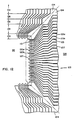
- variable pitch tab leadframe assembly 103 a fragmentary view of a variable pitched tab leadframe assembly 103 is illustrated in which a plurality of substantially identical leadframe assembly segments 104 are shown each comprising patterned conductive elements 107 for transmitting input and output signals to bonding locations 110 on an electronic device.
- Variable pitch tab leadframe assembly 103 also comprises means for providing a variable pitch to conductive elements 107 to accommodate a plurality of standard pitch bond site printed circuit board footprints, such as footprints designated by JEDEC standards.
- Figure 12 shows a fragment of a typical tab leadframe assembly according to the variable pitch leadframe assembly invention and may be appreciated more fully in the context of Figure 13 which illustrates, in dotted lines, the relative relation of the fragment of Figure 12 when combined with other fragments to form a complete representative outline of a typical variable pitch tab leadframe assembly 103 positioned preferably as one of a plurality of such leadframe assemblies on a sprocketed tape 112.
- a central region labelled 116 represents the area in which a die, a semiconductor chip, or the like, is placed for interconnection with variable pitch tab leadframe assembly 103.
- Preferred variable pitch tab leadframe assembly segment 104 comprises means for providing a variable pitch to conductive elements 107, conductive elements 107 each comprising a first end portion 120 arranged for connection with a semiconductor chip package located in area 116. Each conductive element also comprises a second end portion 123, the location of which is selected by the manufacturer, which is arranged for connection with a next level of packaging.
- first end portions 120 of adjacent conductive elements have a first pitch spacing
- second end portions 123 of said adjacent conductive elements have a second pitch spacing which is different than the first pitch spacing.
- this relationship is represented by adjacent conductive elements first and second end portions labelled 120a, 120b, and 123a, 123b respectively.
- Variable pitch tab leadframe assembly segments 104 may comprise a plurality of parallel sections each having a pitch spacing corresponding to, for example, a JEDEC standard pitch spacing commonly used within the field of component packaging.
- the pitch spacing between lead second end portions may be 50 mils (1.25mm), 40 mils (1.0mm), 25 mils (.625mm), 20 mils (0.5mm), or even less.
- the pitch of packaging continues to decrease. Yet each time a different pitch is used on a package, it may require a package leadframe-to-board spacing specifically for that pitch.
- this variable pitch tab leadframe invention provides leadframe assembly segments 104 which comprise conductive elements 107 for connection with a package such that the package may be connected to variously pitched next levels of packaging, and vice versa. This may be accomplished by taking a tightly pitched package and attaching a leadframe to it that has and relies on the tab design to change the leadframe-to-board pitch.
- Tab leadframe assembly segment 104 preferably comprises interconnect sites which are fanned out along each conductive element to various desired pitches. This permits the chip manufacturer to provide a packaged device to a variety of users depending upon the user's sophistication in bonding devices to next levels of packaging using tight pitches.
- variable pitch tab leadframe assemblies 103 may be used on many differently pitched printed circuit boards and package arrangements by cutting conductive elements 107 for desired pitch lengths at second ends 123 from a plurality of preexisting second end pitch patterns on conductive elements 107. This results in substantial savings in that manufacturers do not have to tool new leadframes and packages for each different board or user requirement. It is to be understood that pitch spacing greater than or less than those exemplary pitch spacings indicated above are envisioned within the scope of this invention, as is the number of parallel sections on conductive elements 107 for achieving numerous different pitches.
- Variable pitch tab leadframe assembly 103 for providing connection between a semiconductor chip package, which would be located in area 116, and a next level of packaging, which would be located in an area generally designated 126 corresponding to a printed circuit board or the like.
- Variable pitch tab leadframe assembly 103 also preferably comprises leadframe assembly segments 104 comprising a plurality of patterned conductive elements 107 for transmitting input and output signals to bonding locations on an electronic device.
- Variable pitch tab leadframe assembly 103 also preferably comprises means for providing a variable pitch pattern to conductive elements 107 each comprising a first section 130 and a second section 132 in which adjacent conductive elements are arranged in parallel, and a third section 133 in which adjacent conductive elements 107 are in non-parallel, the first and second sections being connected by the third section.
- each conductive element 107 preferably comprises a first end portion 120 for connection with a semiconductor chip package ahd a second end portion 123 for connection with a next level of packaging. It is to be understood that second end portions 123 may be located at various lengths or pitches, as shown in Figures 12-16.
- First end portions 120 of adjacent conductive elements 107 preferably have a first pitch spacing and second end portions 123 of said adjacent conductive elements 107 have a second pitch spacing which is different than the first pitch spacing.
- the pitch spacing on preferred variable pitch tab leadframe assembly 103 between adjacent conductive elements 107 differs between the first and second sections.
- first end portions 120 of adjacent conductive elements 107 are spaced at any practicable pitch.
- the corresponding second end portions of adjacent conductive elements 107 may be spaced at a pitch of generally between about 5 mils(0.125mm) and 50 mils (1.25mm). It is appreciated that the next level of packaging user will determine the appropriate pitch for leadframe-to-board attach.
- adjacent conductive element second end portions 123 comprise different pitches depending on where the conductive elements 107 are severed, as determined by the pitch of the bond sites at the next level of packaging.
- second end portions 123 are shown positioned at corresponding bond pads 130 having a pitch P1.
- Figure 15 illustrates a next level of packaging requirement with bond pads 140 having a pitch P2 that is different from pitch P1.
- Figure 16 illustrates another packaging requirement for which a pitch P3 exists between bond pads 150.
- No prior art tab leadframe assembly is known or available with structure to accommodate the multiple next level of packaging pitch requirements as depicted in Figures 14-16, or more.
- variable pitch tab leadframe assembly 103 may be used for various pitch requirements with the great advantages of simplicity, material efficiency, and savings of electronic packaging time, and is thus preferred.
- a method of providing a tab leadframe assembly is also provided which permits electrical connection between a semiconductor chip package and a next level of packaging comprising various steps. These steps preferably comprise providing a leadframe as shown substantially as in Figure 12 comprising a plurality of patterned conductive elements; arranging the pattern of the leadframe conductive elements to provide a first section 130, a second section 132, and a third section 134 in which adjacent conductive elements are arranged in parallel, and a fourth section 133 and a fifth section 135 in which adjacent conductive elements are arranged in non-parallel fanned relation and which provide interconnection between the first, second, and third sections.
- the step of arranging the pattern of the leadframe conductive elements may comprise providing a plurality of first, second, and third sections so that the pitch spacing of adjacent conductive elements differs between the first, second, and third sections. Further sections may be included following the above method of manufacture.
Landscapes
- Engineering & Computer Science (AREA)
- Manufacturing & Machinery (AREA)
- Microelectronics & Electronic Packaging (AREA)
- Wire Bonding (AREA)
- Lead Frames For Integrated Circuits (AREA)
- Coupling Device And Connection With Printed Circuit (AREA)
Applications Claiming Priority (2)
| Application Number | Priority Date | Filing Date | Title |
|---|---|---|---|
| US07/341,638 US4999700A (en) | 1989-04-20 | 1989-04-20 | Package to board variable pitch tab |
| US341638 | 2003-01-14 |
Publications (3)
| Publication Number | Publication Date |
|---|---|
| EP0393997A2 true EP0393997A2 (fr) | 1990-10-24 |
| EP0393997A3 EP0393997A3 (fr) | 1991-04-17 |
| EP0393997B1 EP0393997B1 (fr) | 1995-02-01 |
Family
ID=23338407
Family Applications (1)
| Application Number | Title | Priority Date | Filing Date |
|---|---|---|---|
| EP90304121A Expired - Lifetime EP0393997B1 (fr) | 1989-04-20 | 1990-04-18 | Procédé pour fabriquer un boîtier à cadre de connection dont les contacts sont à pas variable |
Country Status (5)
| Country | Link |
|---|---|
| US (1) | US4999700A (fr) |
| EP (1) | EP0393997B1 (fr) |
| JP (1) | JPH0368151A (fr) |
| CA (1) | CA2014871C (fr) |
| DE (1) | DE69016489T2 (fr) |
Cited By (11)
| Publication number | Priority date | Publication date | Assignee | Title |
|---|---|---|---|---|
| SG103824A1 (en) * | 1999-10-15 | 2004-05-26 | Amkor Technology Inc | Leadframe and semiconductor package with improved solder joint strength |
| US8154111B2 (en) | 1999-12-16 | 2012-04-10 | Amkor Technology, Inc. | Near chip size semiconductor package |
| US8866278B1 (en) | 2011-10-10 | 2014-10-21 | Amkor Technology, Inc. | Semiconductor device with increased I/O configuration |
| US9631481B1 (en) | 2011-01-27 | 2017-04-25 | Amkor Technology, Inc. | Semiconductor device including leadframe with a combination of leads and lands and method |
| US9673122B2 (en) | 2014-05-02 | 2017-06-06 | Amkor Technology, Inc. | Micro lead frame structure having reinforcing portions and method |
| US9691734B1 (en) | 2009-12-07 | 2017-06-27 | Amkor Technology, Inc. | Method of forming a plurality of electronic component packages |
| US9704725B1 (en) | 2012-03-06 | 2017-07-11 | Amkor Technology, Inc. | Semiconductor device with leadframe configured to facilitate reduced burr formation |
| US9871015B1 (en) | 2002-11-08 | 2018-01-16 | Amkor Technology, Inc. | Wafer level package and fabrication method |
| US9947623B1 (en) | 2011-11-29 | 2018-04-17 | Amkor Technology, Inc. | Semiconductor device comprising a conductive pad on a protruding-through electrode |
| US10014240B1 (en) | 2012-03-29 | 2018-07-03 | Amkor Technology, Inc. | Embedded component package and fabrication method |
| US10811341B2 (en) | 2009-01-05 | 2020-10-20 | Amkor Technology Singapore Holding Pte Ltd. | Semiconductor device with through-mold via |
Families Citing this family (105)
| Publication number | Priority date | Publication date | Assignee | Title |
|---|---|---|---|---|
| US5168345A (en) * | 1990-08-15 | 1992-12-01 | Lsi Logic Corporation | Semiconductor device having a universal die size inner lead layout |
| US5168344A (en) * | 1990-08-15 | 1992-12-01 | W. R. Grace & Co. Conn. | Ceramic electronic package design |
| US5153507A (en) * | 1990-11-16 | 1992-10-06 | Vlsi Technology, Inc. | Multi-purpose bond pad test die |
| US5266520A (en) * | 1991-02-11 | 1993-11-30 | International Business Machines Corporation | Electronic packaging with varying height connectors |
| US5173763A (en) * | 1991-02-11 | 1992-12-22 | International Business Machines Corporation | Electronic packaging with varying height connectors |
| US5400219A (en) * | 1992-09-02 | 1995-03-21 | Eastman Kodak Company | Tape automated bonding for electrically connecting semiconductor chips to substrates |
| US5336928A (en) * | 1992-09-18 | 1994-08-09 | General Electric Company | Hermetically sealed packaged electronic system |
| JPH07176677A (ja) * | 1993-08-31 | 1995-07-14 | Texas Instr Inc <Ti> | 低コストリードフレームの設計及び製造方法 |
| US6465743B1 (en) * | 1994-12-05 | 2002-10-15 | Motorola, Inc. | Multi-strand substrate for ball-grid array assemblies and method |
| JP3597913B2 (ja) * | 1995-07-20 | 2004-12-08 | 松下電器産業株式会社 | 半導体装置とその実装方法 |
| JP3870301B2 (ja) * | 1996-06-11 | 2007-01-17 | ヤマハ株式会社 | 半導体装置の組立法、半導体装置及び半導体装置の連続組立システム |
| DE19652395A1 (de) * | 1996-06-13 | 1997-12-18 | Samsung Electronics Co Ltd | Integrierte Schaltkreisanordnung |
| US5776798A (en) * | 1996-09-04 | 1998-07-07 | Motorola, Inc. | Semiconductor package and method thereof |
| US7071541B1 (en) | 1998-06-24 | 2006-07-04 | Amkor Technology, Inc. | Plastic integrated circuit package and method and leadframe for making the package |
| US7030474B1 (en) | 1998-06-24 | 2006-04-18 | Amkor Technology, Inc. | Plastic integrated circuit package and method and leadframe for making the package |
| US6143981A (en) | 1998-06-24 | 2000-11-07 | Amkor Technology, Inc. | Plastic integrated circuit package and method and leadframe for making the package |
| US7112474B1 (en) | 1998-06-24 | 2006-09-26 | Amkor Technology, Inc. | Method of making an integrated circuit package |
| US7332375B1 (en) | 1998-06-24 | 2008-02-19 | Amkor Technology, Inc. | Method of making an integrated circuit package |
| US7005326B1 (en) | 1998-06-24 | 2006-02-28 | Amkor Technology, Inc. | Method of making an integrated circuit package |
| US6893900B1 (en) | 1998-06-24 | 2005-05-17 | Amkor Technology, Inc. | Method of making an integrated circuit package |
| US6448633B1 (en) | 1998-11-20 | 2002-09-10 | Amkor Technology, Inc. | Semiconductor package and method of making using leadframe having lead locks to secure leads to encapsulant |
| KR100403142B1 (ko) | 1999-10-15 | 2003-10-30 | 앰코 테크놀로지 코리아 주식회사 | 반도체패키지 |
| KR20010037247A (ko) | 1999-10-15 | 2001-05-07 | 마이클 디. 오브라이언 | 반도체패키지 |
| US6580159B1 (en) | 1999-11-05 | 2003-06-17 | Amkor Technology, Inc. | Integrated circuit device packages and substrates for making the packages |
| US6847103B1 (en) | 1999-11-09 | 2005-01-25 | Amkor Technology, Inc. | Semiconductor package with exposed die pad and body-locking leadframe |
| KR100421774B1 (ko) | 1999-12-16 | 2004-03-10 | 앰코 테크놀로지 코리아 주식회사 | 반도체패키지 및 그 제조 방법 |
| KR100583494B1 (ko) | 2000-03-25 | 2006-05-24 | 앰코 테크놀로지 코리아 주식회사 | 반도체패키지 |
| US7042068B2 (en) | 2000-04-27 | 2006-05-09 | Amkor Technology, Inc. | Leadframe and semiconductor package made using the leadframe |
| KR20020058209A (ko) | 2000-12-29 | 2002-07-12 | 마이클 디. 오브라이언 | 반도체패키지 |
| US6967395B1 (en) | 2001-03-20 | 2005-11-22 | Amkor Technology, Inc. | Mounting for a package containing a chip |
| KR100369393B1 (ko) | 2001-03-27 | 2003-02-05 | 앰코 테크놀로지 코리아 주식회사 | 리드프레임 및 이를 이용한 반도체패키지와 그 제조 방법 |
| KR100393448B1 (ko) | 2001-03-27 | 2003-08-02 | 앰코 테크놀로지 코리아 주식회사 | 반도체 패키지 및 그 제조 방법 |
| US7045883B1 (en) | 2001-04-04 | 2006-05-16 | Amkor Technology, Inc. | Thermally enhanced chip scale lead on chip semiconductor package and method of making same |
| US7064009B1 (en) | 2001-04-04 | 2006-06-20 | Amkor Technology, Inc. | Thermally enhanced chip scale lead on chip semiconductor package and method of making same |
| US6597059B1 (en) | 2001-04-04 | 2003-07-22 | Amkor Technology, Inc. | Thermally enhanced chip scale lead on chip semiconductor package |
| US6900527B1 (en) | 2001-09-19 | 2005-05-31 | Amkor Technology, Inc. | Lead-frame method and assembly for interconnecting circuits within a circuit module |
| US7485952B1 (en) | 2001-09-19 | 2009-02-03 | Amkor Technology, Inc. | Drop resistant bumpers for fully molded memory cards |
| US6630726B1 (en) | 2001-11-07 | 2003-10-07 | Amkor Technology, Inc. | Power semiconductor package with strap |
| US6608366B1 (en) | 2002-04-15 | 2003-08-19 | Harry J. Fogelson | Lead frame with plated end leads |
| US6818973B1 (en) | 2002-09-09 | 2004-11-16 | Amkor Technology, Inc. | Exposed lead QFP package fabricated through the use of a partial saw process |
| US7190062B1 (en) | 2004-06-15 | 2007-03-13 | Amkor Technology, Inc. | Embedded leadframe semiconductor package |
| US7723210B2 (en) | 2002-11-08 | 2010-05-25 | Amkor Technology, Inc. | Direct-write wafer level chip scale package |
| US7361533B1 (en) | 2002-11-08 | 2008-04-22 | Amkor Technology, Inc. | Stacked embedded leadframe |
| US6847099B1 (en) | 2003-02-05 | 2005-01-25 | Amkor Technology Inc. | Offset etched corner leads for semiconductor package |
| US6794740B1 (en) | 2003-03-13 | 2004-09-21 | Amkor Technology, Inc. | Leadframe package for semiconductor devices |
| US7001799B1 (en) | 2003-03-13 | 2006-02-21 | Amkor Technology, Inc. | Method of making a leadframe for semiconductor devices |
| US6879034B1 (en) | 2003-05-01 | 2005-04-12 | Amkor Technology, Inc. | Semiconductor package including low temperature co-fired ceramic substrate |
| US7008825B1 (en) | 2003-05-27 | 2006-03-07 | Amkor Technology, Inc. | Leadframe strip having enhanced testability |
| US6897550B1 (en) | 2003-06-11 | 2005-05-24 | Amkor Technology, Inc. | Fully-molded leadframe stand-off feature |
| US7245007B1 (en) | 2003-09-18 | 2007-07-17 | Amkor Technology, Inc. | Exposed lead interposer leadframe package |
| US6921967B2 (en) | 2003-09-24 | 2005-07-26 | Amkor Technology, Inc. | Reinforced die pad support structure |
| US7138707B1 (en) | 2003-10-21 | 2006-11-21 | Amkor Technology, Inc. | Semiconductor package including leads and conductive posts for providing increased functionality |
| US7144517B1 (en) | 2003-11-07 | 2006-12-05 | Amkor Technology, Inc. | Manufacturing method for leadframe and for semiconductor package using the leadframe |
| US7211879B1 (en) | 2003-11-12 | 2007-05-01 | Amkor Technology, Inc. | Semiconductor package with chamfered corners and method of manufacturing the same |
| US7057268B1 (en) | 2004-01-27 | 2006-06-06 | Amkor Technology, Inc. | Cavity case with clip/plug for use on multi-media card |
| US7091594B1 (en) | 2004-01-28 | 2006-08-15 | Amkor Technology, Inc. | Leadframe type semiconductor package having reduced inductance and its manufacturing method |
| KR100642748B1 (ko) * | 2004-07-24 | 2006-11-10 | 삼성전자주식회사 | 리드 프레임과 패키지 기판 및 이들을 이용한 패키지 |
| US7202554B1 (en) | 2004-08-19 | 2007-04-10 | Amkor Technology, Inc. | Semiconductor package and its manufacturing method |
| US7217991B1 (en) | 2004-10-22 | 2007-05-15 | Amkor Technology, Inc. | Fan-in leadframe semiconductor package |
| US7507603B1 (en) | 2005-12-02 | 2009-03-24 | Amkor Technology, Inc. | Etch singulated semiconductor package |
| US7572681B1 (en) | 2005-12-08 | 2009-08-11 | Amkor Technology, Inc. | Embedded electronic component package |
| US7902660B1 (en) | 2006-05-24 | 2011-03-08 | Amkor Technology, Inc. | Substrate for semiconductor device and manufacturing method thereof |
| US7968998B1 (en) | 2006-06-21 | 2011-06-28 | Amkor Technology, Inc. | Side leaded, bottom exposed pad and bottom exposed lead fusion quad flat semiconductor package |
| US7687893B2 (en) | 2006-12-27 | 2010-03-30 | Amkor Technology, Inc. | Semiconductor package having leadframe with exposed anchor pads |
| US7829990B1 (en) | 2007-01-18 | 2010-11-09 | Amkor Technology, Inc. | Stackable semiconductor package including laminate interposer |
| US7982297B1 (en) | 2007-03-06 | 2011-07-19 | Amkor Technology, Inc. | Stackable semiconductor package having partially exposed semiconductor die and method of fabricating the same |
| US7977774B2 (en) | 2007-07-10 | 2011-07-12 | Amkor Technology, Inc. | Fusion quad flat semiconductor package |
| US7687899B1 (en) | 2007-08-07 | 2010-03-30 | Amkor Technology, Inc. | Dual laminate package structure with embedded elements |
| US7777351B1 (en) | 2007-10-01 | 2010-08-17 | Amkor Technology, Inc. | Thin stacked interposer package |
| US8089159B1 (en) | 2007-10-03 | 2012-01-03 | Amkor Technology, Inc. | Semiconductor package with increased I/O density and method of making the same |
| US7847386B1 (en) | 2007-11-05 | 2010-12-07 | Amkor Technology, Inc. | Reduced size stacked semiconductor package and method of making the same |
| US7956453B1 (en) | 2008-01-16 | 2011-06-07 | Amkor Technology, Inc. | Semiconductor package with patterning layer and method of making same |
| US7723852B1 (en) | 2008-01-21 | 2010-05-25 | Amkor Technology, Inc. | Stacked semiconductor package and method of making same |
| US8067821B1 (en) | 2008-04-10 | 2011-11-29 | Amkor Technology, Inc. | Flat semiconductor package with half package molding |
| US7768135B1 (en) | 2008-04-17 | 2010-08-03 | Amkor Technology, Inc. | Semiconductor package with fast power-up cycle and method of making same |
| US7808084B1 (en) | 2008-05-06 | 2010-10-05 | Amkor Technology, Inc. | Semiconductor package with half-etched locking features |
| US8125064B1 (en) | 2008-07-28 | 2012-02-28 | Amkor Technology, Inc. | Increased I/O semiconductor package and method of making same |
| US8184453B1 (en) | 2008-07-31 | 2012-05-22 | Amkor Technology, Inc. | Increased capacity semiconductor package |
| US7847392B1 (en) | 2008-09-30 | 2010-12-07 | Amkor Technology, Inc. | Semiconductor device including leadframe with increased I/O |
| US7989933B1 (en) | 2008-10-06 | 2011-08-02 | Amkor Technology, Inc. | Increased I/O leadframe and semiconductor device including same |
| US8008758B1 (en) | 2008-10-27 | 2011-08-30 | Amkor Technology, Inc. | Semiconductor device with increased I/O leadframe |
| US8089145B1 (en) | 2008-11-17 | 2012-01-03 | Amkor Technology, Inc. | Semiconductor device including increased capacity leadframe |
| US8072050B1 (en) | 2008-11-18 | 2011-12-06 | Amkor Technology, Inc. | Semiconductor device with increased I/O leadframe including passive device |
| US7875963B1 (en) | 2008-11-21 | 2011-01-25 | Amkor Technology, Inc. | Semiconductor device including leadframe having power bars and increased I/O |
| US7982298B1 (en) | 2008-12-03 | 2011-07-19 | Amkor Technology, Inc. | Package in package semiconductor device |
| US8487420B1 (en) | 2008-12-08 | 2013-07-16 | Amkor Technology, Inc. | Package in package semiconductor device with film over wire |
| US8680656B1 (en) | 2009-01-05 | 2014-03-25 | Amkor Technology, Inc. | Leadframe structure for concentrated photovoltaic receiver package |
| US8058715B1 (en) | 2009-01-09 | 2011-11-15 | Amkor Technology, Inc. | Package in package device for RF transceiver module |
| US8026589B1 (en) | 2009-02-23 | 2011-09-27 | Amkor Technology, Inc. | Reduced profile stackable semiconductor package |
| US7960818B1 (en) | 2009-03-04 | 2011-06-14 | Amkor Technology, Inc. | Conformal shield on punch QFN semiconductor package |
| US8575742B1 (en) | 2009-04-06 | 2013-11-05 | Amkor Technology, Inc. | Semiconductor device with increased I/O leadframe including power bars |
| US8796561B1 (en) | 2009-10-05 | 2014-08-05 | Amkor Technology, Inc. | Fan out build up substrate stackable package and method |
| US8937381B1 (en) | 2009-12-03 | 2015-01-20 | Amkor Technology, Inc. | Thin stackable package and method |
| US8324511B1 (en) | 2010-04-06 | 2012-12-04 | Amkor Technology, Inc. | Through via nub reveal method and structure |
| US8294276B1 (en) | 2010-05-27 | 2012-10-23 | Amkor Technology, Inc. | Semiconductor device and fabricating method thereof |
| US8440554B1 (en) | 2010-08-02 | 2013-05-14 | Amkor Technology, Inc. | Through via connected backside embedded circuit features structure and method |
| US8487445B1 (en) | 2010-10-05 | 2013-07-16 | Amkor Technology, Inc. | Semiconductor device having through electrodes protruding from dielectric layer |
| US8791501B1 (en) | 2010-12-03 | 2014-07-29 | Amkor Technology, Inc. | Integrated passive device structure and method |
| US8674485B1 (en) | 2010-12-08 | 2014-03-18 | Amkor Technology, Inc. | Semiconductor device including leadframe with downsets |
| US8390130B1 (en) | 2011-01-06 | 2013-03-05 | Amkor Technology, Inc. | Through via recessed reveal structure and method |
| US8648450B1 (en) | 2011-01-27 | 2014-02-11 | Amkor Technology, Inc. | Semiconductor device including leadframe with a combination of leads and lands |
| US9048298B1 (en) | 2012-03-29 | 2015-06-02 | Amkor Technology, Inc. | Backside warpage control structure and fabrication method |
| US8674504B2 (en) * | 2012-05-21 | 2014-03-18 | Texas Systems Incorporated | Wire-based methodology of widening the pitch of semiconductor chip terminals |
| KR101486790B1 (ko) | 2013-05-02 | 2015-01-28 | 앰코 테크놀로지 코리아 주식회사 | 강성보강부를 갖는 마이크로 리드프레임 |
| KR101563911B1 (ko) | 2013-10-24 | 2015-10-28 | 앰코 테크놀로지 코리아 주식회사 | 반도체 패키지 |
Family Cites Families (11)
| Publication number | Priority date | Publication date | Assignee | Title |
|---|---|---|---|---|
| JPS5571053A (en) * | 1978-11-24 | 1980-05-28 | Hitachi Ltd | Circuit device |
| JPS5720440A (en) * | 1980-06-13 | 1982-02-02 | Nec Corp | Semiconductor device |
| JPS6059745B2 (ja) * | 1980-12-03 | 1985-12-26 | 日本電気株式会社 | リ−ド・フレ−ム |
| JPS5816555A (ja) * | 1981-07-22 | 1983-01-31 | Nec Corp | リ−ドフレ−ム |
| DE3234745C2 (de) * | 1982-09-20 | 1986-03-06 | Siemens AG, 1000 Berlin und 8000 München | Verfahren zur Handhabung von filmmontierten integrierten Schaltkreisen und Vorrichtung zu seiner Durchführung |
| JPS60149079A (ja) * | 1984-01-13 | 1985-08-06 | シャープ株式会社 | 表示体ユニツト接続装置 |
| JPS61154056A (ja) * | 1984-12-26 | 1986-07-12 | Fujitsu Ltd | ボンデイングパツト |
| US4760335A (en) * | 1985-07-30 | 1988-07-26 | Westinghouse Electric Corp. | Large scale integrated circuit test system |
| GB2178895B (en) * | 1985-08-06 | 1988-11-23 | Gen Electric Co Plc | Improved preparation of fragile devices |
| US4795694A (en) * | 1986-06-20 | 1989-01-03 | Siemens Aktiengesellschaft | Manufacture of fine structures for semiconductor contacting |
| JPS6481253A (en) * | 1987-09-22 | 1989-03-27 | Nec Corp | Package of semiconductor integrated circuit |
-
1989
- 1989-04-20 US US07/341,638 patent/US4999700A/en not_active Expired - Lifetime
-
1990
- 1990-04-18 DE DE69016489T patent/DE69016489T2/de not_active Expired - Fee Related
- 1990-04-18 EP EP90304121A patent/EP0393997B1/fr not_active Expired - Lifetime
- 1990-04-19 CA CA002014871A patent/CA2014871C/fr not_active Expired - Lifetime
- 1990-04-20 JP JP2103220A patent/JPH0368151A/ja active Pending
Cited By (20)
| Publication number | Priority date | Publication date | Assignee | Title |
|---|---|---|---|---|
| SG103824A1 (en) * | 1999-10-15 | 2004-05-26 | Amkor Technology Inc | Leadframe and semiconductor package with improved solder joint strength |
| US7102208B1 (en) | 1999-10-15 | 2006-09-05 | Amkor Technology, Inc. | Leadframe and semiconductor package with improved solder joint strength |
| US8154111B2 (en) | 1999-12-16 | 2012-04-10 | Amkor Technology, Inc. | Near chip size semiconductor package |
| US10665567B1 (en) | 2002-11-08 | 2020-05-26 | Amkor Technology, Inc. | Wafer level package and fabrication method |
| US9871015B1 (en) | 2002-11-08 | 2018-01-16 | Amkor Technology, Inc. | Wafer level package and fabrication method |
| US12494414B2 (en) | 2009-01-05 | 2025-12-09 | Amkor Technology Singapore Holding Pte. Ltd. | Semiconductor device with through-mold via |
| US11869829B2 (en) | 2009-01-05 | 2024-01-09 | Amkor Technology Singapore Holding Pte. Ltd. | Semiconductor device with through-mold via |
| US10811341B2 (en) | 2009-01-05 | 2020-10-20 | Amkor Technology Singapore Holding Pte Ltd. | Semiconductor device with through-mold via |
| US9691734B1 (en) | 2009-12-07 | 2017-06-27 | Amkor Technology, Inc. | Method of forming a plurality of electronic component packages |
| US10546833B2 (en) | 2009-12-07 | 2020-01-28 | Amkor Technology, Inc. | Method of forming a plurality of electronic component packages |
| US9978695B1 (en) | 2011-01-27 | 2018-05-22 | Amkor Technology, Inc. | Semiconductor device including leadframe with a combination of leads and lands and method |
| US9631481B1 (en) | 2011-01-27 | 2017-04-25 | Amkor Technology, Inc. | Semiconductor device including leadframe with a combination of leads and lands and method |
| US8866278B1 (en) | 2011-10-10 | 2014-10-21 | Amkor Technology, Inc. | Semiconductor device with increased I/O configuration |
| US10410967B1 (en) | 2011-11-29 | 2019-09-10 | Amkor Technology, Inc. | Electronic device comprising a conductive pad on a protruding-through electrode |
| US9947623B1 (en) | 2011-11-29 | 2018-04-17 | Amkor Technology, Inc. | Semiconductor device comprising a conductive pad on a protruding-through electrode |
| US11043458B2 (en) | 2011-11-29 | 2021-06-22 | Amkor Technology Singapore Holding Pte. Ltd. | Method of manufacturing an electronic device comprising a conductive pad on a protruding-through electrode |
| US10090228B1 (en) | 2012-03-06 | 2018-10-02 | Amkor Technology, Inc. | Semiconductor device with leadframe configured to facilitate reduced burr formation |
| US9704725B1 (en) | 2012-03-06 | 2017-07-11 | Amkor Technology, Inc. | Semiconductor device with leadframe configured to facilitate reduced burr formation |
| US10014240B1 (en) | 2012-03-29 | 2018-07-03 | Amkor Technology, Inc. | Embedded component package and fabrication method |
| US9673122B2 (en) | 2014-05-02 | 2017-06-06 | Amkor Technology, Inc. | Micro lead frame structure having reinforcing portions and method |
Also Published As
| Publication number | Publication date |
|---|---|
| CA2014871C (fr) | 2000-07-04 |
| US4999700A (en) | 1991-03-12 |
| CA2014871A1 (fr) | 1990-10-20 |
| EP0393997A3 (fr) | 1991-04-17 |
| DE69016489T2 (de) | 1995-09-14 |
| EP0393997B1 (fr) | 1995-02-01 |
| JPH0368151A (ja) | 1991-03-25 |
| DE69016489D1 (de) | 1995-03-16 |
Similar Documents
| Publication | Publication Date | Title |
|---|---|---|
| US4999700A (en) | Package to board variable pitch tab | |
| US5139610A (en) | Method of making a surface etched shadow mask | |
| US6800505B2 (en) | Semiconductor device including edge bond pads and related methods | |
| EP0704895B1 (fr) | Procédé de fabrication d'un dispositif semi-conducteur et d'un substrat semi-conducteur | |
| US5872404A (en) | Interconnect bump for flip-chip integrated circuit including integral standoff and hourglass shaped solder coating | |
| US5918364A (en) | Method of forming electrically conductive polymer interconnects on electrical substrates | |
| JP3262497B2 (ja) | チップ実装回路カード構造 | |
| US6919642B2 (en) | Method for bonding IC chips to substrates incorporating dummy bumps and non-conductive adhesive and structures formed | |
| US20090289360A1 (en) | Workpiece contact pads with elevated ring for restricting horizontal movement of terminals of ic during pressing | |
| KR960006967B1 (ko) | 전자부품의 전극과 리드의 접합방법 | |
| US6344234B1 (en) | Method for forming reflowed solder ball with low melting point metal cap | |
| JP3393755B2 (ja) | 低融点金属キャップを有するリフローはんだボールによる相互接続構造 | |
| US7125789B2 (en) | Composite metal column for mounting semiconductor device | |
| US5650667A (en) | Process of forming conductive bumps on the electrodes of semiconductor chips using lapping and the bumps thereby created | |
| US6214156B1 (en) | Semiconductor device mounted on board by flip-chip and method for mounting the same | |
| KR20010060183A (ko) | Ic 디바이스 패키지 제조 방법 | |
| US6396155B1 (en) | Semiconductor device and method of producing the same | |
| US4980240A (en) | Surface etched shadow mask | |
| US5505367A (en) | Method for bumping silicon devices | |
| US20030189245A1 (en) | Flip chip assembly and method for producing the same | |
| US7550852B2 (en) | Composite metal column for mounting semiconductor device | |
| EP0359228A2 (fr) | Liaison eutectique d'or/étain pour le procédé automatique à bande | |
| JP2000294586A (ja) | 半導体装置及び半導体装置の製造方法 | |
| JP2822506B2 (ja) | 半導体装置の製造方法 | |
| JPH05235108A (ja) | フィルムキャリアテープの製造方法 |
Legal Events
| Date | Code | Title | Description |
|---|---|---|---|
| PUAI | Public reference made under article 153(3) epc to a published international application that has entered the european phase |
Free format text: ORIGINAL CODE: 0009012 |
|
| AK | Designated contracting states |
Kind code of ref document: A2 Designated state(s): DE FR GB |
|
| PUAL | Search report despatched |
Free format text: ORIGINAL CODE: 0009013 |
|
| AK | Designated contracting states |
Kind code of ref document: A3 Designated state(s): DE FR GB |
|
| 17P | Request for examination filed |
Effective date: 19910930 |
|
| 17Q | First examination report despatched |
Effective date: 19930507 |
|
| GRAA | (expected) grant |
Free format text: ORIGINAL CODE: 0009210 |
|
| AK | Designated contracting states |
Kind code of ref document: B1 Designated state(s): DE FR GB |
|
| REF | Corresponds to: |
Ref document number: 69016489 Country of ref document: DE Date of ref document: 19950316 |
|
| ET | Fr: translation filed | ||
| PLBE | No opposition filed within time limit |
Free format text: ORIGINAL CODE: 0009261 |
|
| STAA | Information on the status of an ep patent application or granted ep patent |
Free format text: STATUS: NO OPPOSITION FILED WITHIN TIME LIMIT |
|
| 26N | No opposition filed | ||
| REG | Reference to a national code |
Ref country code: GB Ref legal event code: IF02 |
|
| PGFP | Annual fee paid to national office [announced via postgrant information from national office to epo] |
Ref country code: DE Payment date: 20080424 Year of fee payment: 19 Ref country code: FR Payment date: 20080312 Year of fee payment: 19 |
|
| PGFP | Annual fee paid to national office [announced via postgrant information from national office to epo] |
Ref country code: GB Payment date: 20080423 Year of fee payment: 19 |
|
| GBPC | Gb: european patent ceased through non-payment of renewal fee |
Effective date: 20090418 |
|
| REG | Reference to a national code |
Ref country code: FR Ref legal event code: ST Effective date: 20091231 |
|
| PG25 | Lapsed in a contracting state [announced via postgrant information from national office to epo] |
Ref country code: DE Free format text: LAPSE BECAUSE OF NON-PAYMENT OF DUE FEES Effective date: 20091103 |
|
| PG25 | Lapsed in a contracting state [announced via postgrant information from national office to epo] |
Ref country code: GB Free format text: LAPSE BECAUSE OF NON-PAYMENT OF DUE FEES Effective date: 20090418 Ref country code: FR Free format text: LAPSE BECAUSE OF NON-PAYMENT OF DUE FEES Effective date: 20091222 |