EP0394205A2 - Federnder Steckverbinder für Radiofrequenzsignale - Google Patents
Federnder Steckverbinder für Radiofrequenzsignale Download PDFInfo
- Publication number
- EP0394205A2 EP0394205A2 EP90850105A EP90850105A EP0394205A2 EP 0394205 A2 EP0394205 A2 EP 0394205A2 EP 90850105 A EP90850105 A EP 90850105A EP 90850105 A EP90850105 A EP 90850105A EP 0394205 A2 EP0394205 A2 EP 0394205A2
- Authority
- EP
- European Patent Office
- Prior art keywords
- connector
- contact
- contact means
- pin
- printed board
- Prior art date
- Legal status (The legal status is an assumption and is not a legal conclusion. Google has not performed a legal analysis and makes no representation as to the accuracy of the status listed.)
- Granted
Links
- 239000004020 conductor Substances 0.000 description 5
- 238000010276 construction Methods 0.000 description 4
- 230000008878 coupling Effects 0.000 description 1
- 238000010168 coupling process Methods 0.000 description 1
- 238000005859 coupling reaction Methods 0.000 description 1
- 239000002184 metal Substances 0.000 description 1
- 238000000034 method Methods 0.000 description 1
- 238000005476 soldering Methods 0.000 description 1
- 230000008961 swelling Effects 0.000 description 1
Images
Classifications
-
- H—ELECTRICITY
- H01—ELECTRIC ELEMENTS
- H01R—ELECTRICALLY-CONDUCTIVE CONNECTIONS; STRUCTURAL ASSOCIATIONS OF A PLURALITY OF MUTUALLY-INSULATED ELECTRICAL CONNECTING ELEMENTS; COUPLING DEVICES; CURRENT COLLECTORS
- H01R13/00—Details of coupling devices of the kinds covered by groups H01R12/70 or H01R24/00 - H01R33/00
- H01R13/02—Contact members
- H01R13/22—Contacts for co-operating by abutting
- H01R13/24—Contacts for co-operating by abutting resilient; resiliently-mounted
- H01R13/2464—Contacts for co-operating by abutting resilient; resiliently-mounted characterized by the contact point
- H01R13/2471—Contacts for co-operating by abutting resilient; resiliently-mounted characterized by the contact point pin shaped
Definitions
- the invention relates to a connector for radio frequency signals mounted on a printed board in accordance with the introduction of claim 1.
- coaxial connectors are used to connect radio frequency signals, which are carried on a central contact of the connector.
- the signal contact is then coaxially surrounded by a cylindrical contact part providing the earthing and the contact for the sheath.
- a connection comprises two coaxial connectors, a male and a female connector exactly fitting into each other.
- a connector of this type can also be mounted on a printed board.
- the known connectors are reliable but expensive due to their construction.
- the connection of the signal circuits of two printed boards through these connectors further requires an accurate mechanical fitting and a somewhat resilient construction of the mounting, which increases the cost of the connector.
- the applicant has developed a surface connector, in which the contacts consist of the printed conductors of the printed board, so that the contacts for the earthing and the sheath are symmetrically situated on both sides of the signal contact.
- the contacts are located on the surface of the printed board or on an edge of the printed board, perpendicular to the surface of the board.
- One of the connectors of the connection should be a planar connector, the contacts of which can resiliently yield so that the possibility of movement on one hand compensates for any inaccuracies and so that the spring force on the other hand ensures an adequate contact force between the connectors. It should be possible to connect such a new connector against the surface connector, either in the direction of the plane of the board or perpendicular to the board.
- the object of the present invention is to provide such a resilient connector, which makes possible the described connection to a surface connector.
- the object is accomplished by a resilient connector according to the characterizing clause of claim 1.
- the sheath contact means are located symmetrically on both sides of the signal contact means, resiliently yielding in the direction of said plane when the connector is connected to the other connector of the connection.
- the contact means are contact pins, which can move in holes made in the board, each pin being connected to circuits on the printed board through signal springs rubbing the pin with one end, the other end of the spring being connected to a printed circuit, and the contact between the pin and the contact means of the other connector of the connection being secured by another contact spring.
- the contact means are contact springs with one end connected to a printed circuit, the other end having a pin-like projection, the contact between the projection and the contact means of the other connector being secured by the contact spring.
- the contact means of the connector according to the invention are dimensioned and located at a mutual distance such that the impedance level of the connector is low, preferably in the range between 50 and 150 ohms.
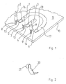
- a printed board 10 is provided with a resilient connector with contacts formed by contact pins 1 - 3 mounted in corresponding holes 12 - 14, which are drilled through the printed board so that the pins can move substantially perpendicular to the plane 11 of the board.
- the pin 1 is the signal contact.
- the contacts 2 and 3 are located symmetrically on both sides of the signal contact.
- the signal and earth connections between the conductors 15 - 17 on the board and the pins 1 - 3 is provided by the signal springs 4 - 6.
- the signal springs comprise a strip of metal with one end 18 (shown for spring 6 only) electrically conducting connected by e.g. soldering with the conductors 15 - 17, the other end rubbing the corresponding pin 1 - 3.
- the contact pin may be provided with a swelling 19 in the rubbing area, as is shown in figure 1.
- the other connector of the connection comprises conductors printed on e.g. a second board so that the printed contacts of the earth and sheath are located symmetrically on both sides of the signal contact, and so that the planar contacts lie in the same plane forming a surface connector.
- the surface connector is described in the application FI 891744, filed simultaneously with the present application.
- the contact pins 1 - 3 according to the present invention will resiliently contact the contacts of the surface connector, so that the possibility of movement on one hand compensates for any inaccuracies and so that the spring force of the helical springs 7 - 9 on the other hand ensures an adequate contact force between the connectors.
- FIG 2 illustrates the possibility to realize the connector according to the invention in an easy way with contact springs 20, of which there would be three in a connector according to figure 1.
- the springs 20 replace the contact pins 1 - 3, the helical springs 7 - 9 and the signal springs 4 - 6.
- One end of the contact spring is connected to a corresponding printed circuit 15 - 17, the other end having a pin-like projection 21, the contact between the projection and the contact means of the other connector being secured by the spring force of the contact spring 20 itself as the connectors are connected in a pressing relationship against each other.
- the plane of movement of the contact pins 1 - 3 described above, through appropriate mechanical arrangements, may be provided in parallel with the plane of the printed board.
- the signal springs 4 - 6 can be formed in different ways, e.g. as a spring with a U-form holding the contact pin as in jaws.
- the pin-like projection 21 can also perform the resilient movement of the contact in the printed board plane.
- the resilient connector according to the invention constitutes a connector meeting the requirements for radio frequency signals, primarily due to its symmetrical construction.
- the contact pins 1 - 3 may thus be dimensioned (width, thickness, and distances between the conductors) according to methods well known in the art, so that the specific impedance or impedance level of the connector will be e.g. 50 ohms, which is the generally used impedance level on radio frequencies.
- the symmetrical construction will also reduce (or prevent) stray coupling.
- the inventive connector described above may in principle also be realized so that the contact pins are duplicated, or so that there are a plurality of them, depending on the requirements of the circuit design and/or of the mechanical conditions.
Landscapes
- Coupling Device And Connection With Printed Circuit (AREA)
- Details Of Connecting Devices For Male And Female Coupling (AREA)
- Input Circuits Of Receivers And Coupling Of Receivers And Audio Equipment (AREA)
- Circuits Of Receivers In General (AREA)
- Transmitters (AREA)
Priority Applications (1)
| Application Number | Priority Date | Filing Date | Title |
|---|---|---|---|
| AT90850105T ATE98820T1 (de) | 1989-04-12 | 1990-03-16 | Federnder steckverbinder fuer radiofrequenzsignale. |
Applications Claiming Priority (2)
| Application Number | Priority Date | Filing Date | Title |
|---|---|---|---|
| FI891745A FI89842C (fi) | 1989-04-12 | 1989-04-12 | Fjaedrande kontaktdon foer radiofrekventa signaler |
| FI891745 | 1989-04-12 |
Publications (3)
| Publication Number | Publication Date |
|---|---|
| EP0394205A2 true EP0394205A2 (de) | 1990-10-24 |
| EP0394205A3 EP0394205A3 (de) | 1991-03-13 |
| EP0394205B1 EP0394205B1 (de) | 1993-12-15 |
Family
ID=8528232
Family Applications (1)
| Application Number | Title | Priority Date | Filing Date |
|---|---|---|---|
| EP90850105A Expired - Lifetime EP0394205B1 (de) | 1989-04-12 | 1990-03-16 | Federnder Steckverbinder für Radiofrequenzsignale |
Country Status (5)
| Country | Link |
|---|---|
| US (1) | US5059131A (de) |
| EP (1) | EP0394205B1 (de) |
| AT (1) | ATE98820T1 (de) |
| DE (1) | DE69005182T2 (de) |
| FI (1) | FI89842C (de) |
Cited By (3)
| Publication number | Priority date | Publication date | Assignee | Title |
|---|---|---|---|---|
| WO1997005674A1 (en) * | 1995-07-25 | 1997-02-13 | Cinch Connectors Ltd. | Co-axial connector systen |
| US6494743B1 (en) | 1999-07-02 | 2002-12-17 | General Dynamics Information Systems, Inc. | Impedance-controlled connector |
| GB2379096A (en) * | 2001-08-22 | 2003-02-26 | Ubinetics Ltd | Apparatus and method for making an RF connection to an RF module |
Families Citing this family (4)
| Publication number | Priority date | Publication date | Assignee | Title |
|---|---|---|---|---|
| FI98028C (fi) * | 1995-05-03 | 1997-03-25 | Nokia Mobile Phones Ltd | Datasovitin |
| GB2316814B (en) * | 1996-08-30 | 2001-02-28 | Nokia Mobile Phones Ltd | A radio telephone connector |
| DE59712744D1 (de) * | 1996-12-13 | 2006-11-23 | Fuba Automotive Gmbh | Leitungs-Steckverbindung |
| FI114839B (fi) * | 1997-12-01 | 2004-12-31 | Nokia Corp | Menetelmä tehonsyötön järjestämiseksi laajennuskortilla |
Family Cites Families (12)
| Publication number | Priority date | Publication date | Assignee | Title |
|---|---|---|---|---|
| DE1085209B (de) * | 1959-12-12 | 1960-07-14 | Dielektra Ag | Gedruckte elektrische Leiterplatte |
| US3248779A (en) * | 1963-11-15 | 1966-05-03 | Leonard J Yuska | Method of making an electronic module |
| DE1208375B (de) * | 1964-03-25 | 1966-01-05 | Telefonbau | Verfahren zur Verbindung von Leitungen beiderseitig bedruckter Leiterplatten |
| GB1150233A (en) * | 1966-09-19 | 1969-04-30 | Clarke & Smith Controls Ltd | Improvements in or relating to Electrical Connectintg Devices. |
| DE1903088A1 (de) * | 1969-01-22 | 1971-01-21 | Siemens Ag | Kontaktvorrichtung |
| US3745510A (en) * | 1971-07-02 | 1973-07-10 | Interdyne Co | Printed circuit board/integrated circuit socket combination |
| US3848947A (en) * | 1972-06-16 | 1974-11-19 | Dot Co Inc | Electrical circuit board terminal springclip |
| SU906046A1 (ru) * | 1977-06-14 | 1982-02-15 | Предприятие П/Я М-5769 | Устройство дл контрол печатных плат |
| US4138179A (en) * | 1977-12-20 | 1979-02-06 | Med General, Inc. | Coaxial jack for printed circuit boards |
| FR2503977A1 (fr) * | 1981-04-10 | 1982-10-15 | Radiotechnique Compelec | Procede de realisation d'une metallisation sur la tranche d'un support plat, et circuit electronique comportant un tel support |
| US4494816A (en) * | 1983-07-27 | 1985-01-22 | At&T Bell Laboratories | Coaxial cable connector |
| US4764848A (en) * | 1986-11-24 | 1988-08-16 | International Business Machines Corporation | Surface mounted array strain relief device |
-
1989
- 1989-04-12 FI FI891745A patent/FI89842C/fi not_active IP Right Cessation
-
1990
- 1990-03-14 US US07/495,613 patent/US5059131A/en not_active Expired - Lifetime
- 1990-03-16 DE DE69005182T patent/DE69005182T2/de not_active Expired - Fee Related
- 1990-03-16 AT AT90850105T patent/ATE98820T1/de not_active IP Right Cessation
- 1990-03-16 EP EP90850105A patent/EP0394205B1/de not_active Expired - Lifetime
Cited By (3)
| Publication number | Priority date | Publication date | Assignee | Title |
|---|---|---|---|---|
| WO1997005674A1 (en) * | 1995-07-25 | 1997-02-13 | Cinch Connectors Ltd. | Co-axial connector systen |
| US6494743B1 (en) | 1999-07-02 | 2002-12-17 | General Dynamics Information Systems, Inc. | Impedance-controlled connector |
| GB2379096A (en) * | 2001-08-22 | 2003-02-26 | Ubinetics Ltd | Apparatus and method for making an RF connection to an RF module |
Also Published As
| Publication number | Publication date |
|---|---|
| DE69005182D1 (de) | 1994-01-27 |
| FI891745L (fi) | 1990-10-13 |
| FI89842C (fi) | 1993-11-25 |
| US5059131A (en) | 1991-10-22 |
| ATE98820T1 (de) | 1994-01-15 |
| FI89842B (fi) | 1993-08-13 |
| EP0394205A3 (de) | 1991-03-13 |
| EP0394205B1 (de) | 1993-12-15 |
| FI891745A0 (fi) | 1989-04-12 |
| DE69005182T2 (de) | 1994-06-16 |
Similar Documents
| Publication | Publication Date | Title |
|---|---|---|
| EP0395609B1 (de) | Oberflächenverbinder für Radiofrequenzsignale | |
| EP0647088B1 (de) | Elektrischer Verbinder | |
| EP0589492B1 (de) | Elektrische Steckverbinder | |
| US3689865A (en) | Connector | |
| USRE36845E (en) | High density, high bandwidth, coaxial cable, flexible circuit and circuit board connection assembly | |
| US4849689A (en) | Microwave wafer probe having replaceable probe tip | |
| US4070084A (en) | Controlled impedance connector | |
| US4922191A (en) | Electronic testing equipment interconnection assembly | |
| WO2003067711B1 (en) | High speed differential signal edge card connector circuit board layouts | |
| KR19980070470A (ko) | 전기 커넥터 | |
| CN1227005A (zh) | 高频电连接器 | |
| US3356983A (en) | Transmission line cable connector | |
| US5672062A (en) | Electrical connectors | |
| WO2001080376A1 (en) | Electrical connector for reducing crosstalk | |
| US5127838A (en) | Plated electrical connectors | |
| EP0394205B1 (de) | Federnder Steckverbinder für Radiofrequenzsignale | |
| US5211581A (en) | Electrical connector assembly and method therefor | |
| JPH0195472A (ja) | 高速信号用コネクタ | |
| EP0569509B1 (de) | Elektrische verbinder | |
| US6929482B2 (en) | Interconnection arrangement | |
| US4842527A (en) | Contact assembly for interconnecting circuit board and a coaxial connector | |
| JPH06105628B2 (ja) | 電気コネクタにおけるインピーダンスと インダクタンスの制御方法及び装置 | |
| JPS59148289A (ja) | コネクタ | |
| CN222087782U (zh) | 贴片射频滤波器的测试工装 | |
| JP2627517B2 (ja) | 電気コネクタ |
Legal Events
| Date | Code | Title | Description |
|---|---|---|---|
| PUAI | Public reference made under article 153(3) epc to a published international application that has entered the european phase |
Free format text: ORIGINAL CODE: 0009012 |
|
| AK | Designated contracting states |
Kind code of ref document: A2 Designated state(s): AT BE CH DE DK ES FR GB GR IT LI LU NL SE |
|
| PUAL | Search report despatched |
Free format text: ORIGINAL CODE: 0009013 |
|
| AK | Designated contracting states |
Kind code of ref document: A3 Designated state(s): AT BE CH DE DK ES FR GB GR IT LI LU NL SE |
|
| RHK1 | Main classification (correction) |
Ipc: H01R 17/12 |
|
| 17P | Request for examination filed |
Effective date: 19910822 |
|
| 17Q | First examination report despatched |
Effective date: 19920716 |
|
| GRAA | (expected) grant |
Free format text: ORIGINAL CODE: 0009210 |
|
| AK | Designated contracting states |
Kind code of ref document: B1 Designated state(s): AT BE CH DE DK ES FR GB GR IT LI LU NL SE |
|
| PG25 | Lapsed in a contracting state [announced via postgrant information from national office to epo] |
Ref country code: IT Free format text: LAPSE BECAUSE OF FAILURE TO SUBMIT A TRANSLATION OF THE DESCRIPTION OR TO PAY THE FEE WITHIN THE PRE;WARNING: LAPSES OF ITALIAN PATENTS WITH EFFECTIVE DATE BEFORE 2007 MAY HAVE OCCURRED AT ANY TIME BEFORE 2007. THE CORRECT EFFECTIVE DATE MAY BE DIFFERENT FROM THE ONE RECORDED.SCRIBED TIME-LIMIT Effective date: 19931215 Ref country code: GR Free format text: LAPSE BECAUSE OF FAILURE TO SUBMIT A TRANSLATION OF THE DESCRIPTION OR TO PAY THE FEE WITHIN THE PRESCRIBED TIME-LIMIT Effective date: 19931215 Ref country code: DK Effective date: 19931215 Ref country code: BE Effective date: 19931215 Ref country code: NL Effective date: 19931215 Ref country code: ES Free format text: THE PATENT HAS BEEN ANNULLED BY A DECISION OF A NATIONAL AUTHORITY Effective date: 19931215 Ref country code: LI Effective date: 19931215 Ref country code: CH Effective date: 19931215 Ref country code: AT Effective date: 19931215 |
|
| REF | Corresponds to: |
Ref document number: 98820 Country of ref document: AT Date of ref document: 19940115 Kind code of ref document: T |
|
| REF | Corresponds to: |
Ref document number: 69005182 Country of ref document: DE Date of ref document: 19940127 |
|
| ET | Fr: translation filed | ||
| PG25 | Lapsed in a contracting state [announced via postgrant information from national office to epo] |
Ref country code: LU Free format text: LAPSE BECAUSE OF NON-PAYMENT OF DUE FEES Effective date: 19940331 |
|
| REG | Reference to a national code |
Ref country code: CH Ref legal event code: PL |
|
| NLV1 | Nl: lapsed or annulled due to failure to fulfill the requirements of art. 29p and 29m of the patents act | ||
| PLBE | No opposition filed within time limit |
Free format text: ORIGINAL CODE: 0009261 |
|
| STAA | Information on the status of an ep patent application or granted ep patent |
Free format text: STATUS: NO OPPOSITION FILED WITHIN TIME LIMIT |
|
| 26N | No opposition filed | ||
| EAL | Se: european patent in force in sweden |
Ref document number: 90850105.9 |
|
| REG | Reference to a national code |
Ref country code: GB Ref legal event code: IF02 |
|
| PGFP | Annual fee paid to national office [announced via postgrant information from national office to epo] |
Ref country code: SE Payment date: 20020306 Year of fee payment: 13 |
|
| PGFP | Annual fee paid to national office [announced via postgrant information from national office to epo] |
Ref country code: FR Payment date: 20020312 Year of fee payment: 13 |
|
| PGFP | Annual fee paid to national office [announced via postgrant information from national office to epo] |
Ref country code: GB Payment date: 20020320 Year of fee payment: 13 |
|
| PGFP | Annual fee paid to national office [announced via postgrant information from national office to epo] |
Ref country code: DE Payment date: 20020327 Year of fee payment: 13 |
|
| REG | Reference to a national code |
Ref country code: GB Ref legal event code: 732E |
|
| PG25 | Lapsed in a contracting state [announced via postgrant information from national office to epo] |
Ref country code: GB Free format text: LAPSE BECAUSE OF NON-PAYMENT OF DUE FEES Effective date: 20030316 |
|
| PG25 | Lapsed in a contracting state [announced via postgrant information from national office to epo] |
Ref country code: SE Free format text: LAPSE BECAUSE OF NON-PAYMENT OF DUE FEES Effective date: 20030317 |
|
| PG25 | Lapsed in a contracting state [announced via postgrant information from national office to epo] |
Ref country code: DE Free format text: LAPSE BECAUSE OF NON-PAYMENT OF DUE FEES Effective date: 20031001 |
|
| EUG | Se: european patent has lapsed | ||
| GBPC | Gb: european patent ceased through non-payment of renewal fee |
Effective date: 20030316 |
|
| PG25 | Lapsed in a contracting state [announced via postgrant information from national office to epo] |
Ref country code: FR Free format text: LAPSE BECAUSE OF NON-PAYMENT OF DUE FEES Effective date: 20031127 |
|
| REG | Reference to a national code |
Ref country code: FR Ref legal event code: ST |