EP0394757A2 - Procédé pour la fabrication de structures semi-conductrices actives utilisant des structures de base avec une couche à porteur de charge bidimensionelle parallèle à sa surface - Google Patents
Procédé pour la fabrication de structures semi-conductrices actives utilisant des structures de base avec une couche à porteur de charge bidimensionelle parallèle à sa surface Download PDFInfo
- Publication number
- EP0394757A2 EP0394757A2 EP90106940A EP90106940A EP0394757A2 EP 0394757 A2 EP0394757 A2 EP 0394757A2 EP 90106940 A EP90106940 A EP 90106940A EP 90106940 A EP90106940 A EP 90106940A EP 0394757 A2 EP0394757 A2 EP 0394757A2
- Authority
- EP
- European Patent Office
- Prior art keywords
- line
- charge carrier
- channel
- carrier layer
- gate
- Prior art date
- Legal status (The legal status is an assumption and is not a legal conclusion. Google has not performed a legal analysis and makes no representation as to the accuracy of the status listed.)
- Granted
Links
Images







Classifications
-
- B—PERFORMING OPERATIONS; TRANSPORTING
- B82—NANOTECHNOLOGY
- B82Y—SPECIFIC USES OR APPLICATIONS OF NANOSTRUCTURES; MEASUREMENT OR ANALYSIS OF NANOSTRUCTURES; MANUFACTURE OR TREATMENT OF NANOSTRUCTURES
- B82Y10/00—Nanotechnology for information processing, storage or transmission, e.g. quantum computing or single electron logic
-
- H—ELECTRICITY
- H10—SEMICONDUCTOR DEVICES; ELECTRIC SOLID-STATE DEVICES NOT OTHERWISE PROVIDED FOR
- H10P—GENERIC PROCESSES OR APPARATUS FOR THE MANUFACTURE OR TREATMENT OF DEVICES COVERED BY CLASS H10
- H10P30/00—Ion implantation into wafers, substrates or parts of devices
- H10P30/20—Ion implantation into wafers, substrates or parts of devices into semiconductor materials, e.g. for doping
- H10P30/21—Ion implantation into wafers, substrates or parts of devices into semiconductor materials, e.g. for doping of electrically active species
-
- H—ELECTRICITY
- H10—SEMICONDUCTOR DEVICES; ELECTRIC SOLID-STATE DEVICES NOT OTHERWISE PROVIDED FOR
- H10D—INORGANIC ELECTRIC SEMICONDUCTOR DEVICES
- H10D1/00—Resistors, capacitors or inductors
- H10D1/40—Resistors
-
- H—ELECTRICITY
- H10—SEMICONDUCTOR DEVICES; ELECTRIC SOLID-STATE DEVICES NOT OTHERWISE PROVIDED FOR
- H10D—INORGANIC ELECTRIC SEMICONDUCTOR DEVICES
- H10D30/00—Field-effect transistors [FET]
- H10D30/01—Manufacture or treatment
- H10D30/014—Manufacture or treatment of FETs having zero-dimensional [0D] or one-dimensional [1D] channels, e.g. quantum wire FETs, single-electron transistors [SET] or Coulomb blockade transistors
-
- H—ELECTRICITY
- H10—SEMICONDUCTOR DEVICES; ELECTRIC SOLID-STATE DEVICES NOT OTHERWISE PROVIDED FOR
- H10D—INORGANIC ELECTRIC SEMICONDUCTOR DEVICES
- H10D30/00—Field-effect transistors [FET]
- H10D30/40—FETs having zero-dimensional [0D], one-dimensional [1D] or two-dimensional [2D] charge carrier gas channels
- H10D30/43—FETs having zero-dimensional [0D], one-dimensional [1D] or two-dimensional [2D] charge carrier gas channels having one-dimensional [1D] charge carrier gas channels, e.g. quantum wire FETs or transistors having 1D quantum-confined channels
-
- H—ELECTRICITY
- H10—SEMICONDUCTOR DEVICES; ELECTRIC SOLID-STATE DEVICES NOT OTHERWISE PROVIDED FOR
- H10D—INORGANIC ELECTRIC SEMICONDUCTOR DEVICES
- H10D62/00—Semiconductor bodies, or regions thereof, of devices having potential barriers
- H10D62/10—Shapes, relative sizes or dispositions of the regions of the semiconductor bodies; Shapes of the semiconductor bodies
- H10D62/113—Isolations within a component, i.e. internal isolations
- H10D62/115—Dielectric isolations, e.g. air gaps
- H10D62/116—Dielectric isolations, e.g. air gaps adjoining the input or output regions of field-effect devices, e.g. adjoining source or drain regions
-
- H—ELECTRICITY
- H10—SEMICONDUCTOR DEVICES; ELECTRIC SOLID-STATE DEVICES NOT OTHERWISE PROVIDED FOR
- H10D—INORGANIC ELECTRIC SEMICONDUCTOR DEVICES
- H10D62/00—Semiconductor bodies, or regions thereof, of devices having potential barriers
- H10D62/50—Physical imperfections
- H10D62/53—Physical imperfections the imperfections being within the semiconductor body
-
- H—ELECTRICITY
- H10—SEMICONDUCTOR DEVICES; ELECTRIC SOLID-STATE DEVICES NOT OTHERWISE PROVIDED FOR
- H10D—INORGANIC ELECTRIC SEMICONDUCTOR DEVICES
- H10D64/00—Electrodes of devices having potential barriers
- H10D64/20—Electrodes characterised by their shapes, relative sizes or dispositions
- H10D64/27—Electrodes not carrying the current to be rectified, amplified, oscillated or switched, e.g. gates
- H10D64/311—Gate electrodes for field-effect devices
- H10D64/411—Gate electrodes for field-effect devices for FETs
- H10D64/511—Gate electrodes for field-effect devices for FETs for IGFETs
- H10D64/517—Gate electrodes for field-effect devices for FETs for IGFETs characterised by the conducting layers
- H10D64/519—Gate electrodes for field-effect devices for FETs for IGFETs characterised by the conducting layers characterised by their top-view geometrical layouts
-
- H—ELECTRICITY
- H10—SEMICONDUCTOR DEVICES; ELECTRIC SOLID-STATE DEVICES NOT OTHERWISE PROVIDED FOR
- H10D—INORGANIC ELECTRIC SEMICONDUCTOR DEVICES
- H10D64/00—Electrodes of devices having potential barriers
- H10D64/60—Electrodes characterised by their materials
- H10D64/66—Electrodes having a conductor capacitively coupled to a semiconductor by an insulator, e.g. MIS electrodes
- H10D64/68—Electrodes having a conductor capacitively coupled to a semiconductor by an insulator, e.g. MIS electrodes characterised by the insulator, e.g. by the gate insulator
- H10D64/691—Electrodes having a conductor capacitively coupled to a semiconductor by an insulator, e.g. MIS electrodes characterised by the insulator, e.g. by the gate insulator comprising metallic compounds, e.g. metal oxides or metal silicates
-
- H—ELECTRICITY
- H10—SEMICONDUCTOR DEVICES; ELECTRIC SOLID-STATE DEVICES NOT OTHERWISE PROVIDED FOR
- H10D—INORGANIC ELECTRIC SEMICONDUCTOR DEVICES
- H10D84/00—Integrated devices formed in or on semiconductor substrates that comprise only semiconducting layers, e.g. on Si wafers or on GaAs-on-Si wafers
- H10D84/01—Manufacture or treatment
-
- H—ELECTRICITY
- H10—SEMICONDUCTOR DEVICES; ELECTRIC SOLID-STATE DEVICES NOT OTHERWISE PROVIDED FOR
- H10D—INORGANIC ELECTRIC SEMICONDUCTOR DEVICES
- H10D84/00—Integrated devices formed in or on semiconductor substrates that comprise only semiconducting layers, e.g. on Si wafers or on GaAs-on-Si wafers
- H10D84/01—Manufacture or treatment
- H10D84/02—Manufacture or treatment characterised by using material-based technologies
- H10D84/05—Manufacture or treatment characterised by using material-based technologies using Group III-V technology
-
- H—ELECTRICITY
- H10—SEMICONDUCTOR DEVICES; ELECTRIC SOLID-STATE DEVICES NOT OTHERWISE PROVIDED FOR
- H10P—GENERIC PROCESSES OR APPARATUS FOR THE MANUFACTURE OR TREATMENT OF DEVICES COVERED BY CLASS H10
- H10P30/00—Ion implantation into wafers, substrates or parts of devices
- H10P30/20—Ion implantation into wafers, substrates or parts of devices into semiconductor materials, e.g. for doping
- H10P30/202—Ion implantation into wafers, substrates or parts of devices into semiconductor materials, e.g. for doping characterised by the semiconductor materials
- H10P30/204—Ion implantation into wafers, substrates or parts of devices into semiconductor materials, e.g. for doping characterised by the semiconductor materials into Group IV semiconductors
-
- H—ELECTRICITY
- H10—SEMICONDUCTOR DEVICES; ELECTRIC SOLID-STATE DEVICES NOT OTHERWISE PROVIDED FOR
- H10P—GENERIC PROCESSES OR APPARATUS FOR THE MANUFACTURE OR TREATMENT OF DEVICES COVERED BY CLASS H10
- H10P30/00—Ion implantation into wafers, substrates or parts of devices
- H10P30/20—Ion implantation into wafers, substrates or parts of devices into semiconductor materials, e.g. for doping
- H10P30/202—Ion implantation into wafers, substrates or parts of devices into semiconductor materials, e.g. for doping characterised by the semiconductor materials
- H10P30/206—Ion implantation into wafers, substrates or parts of devices into semiconductor materials, e.g. for doping characterised by the semiconductor materials into Group III-V semiconductors
-
- H—ELECTRICITY
- H10—SEMICONDUCTOR DEVICES; ELECTRIC SOLID-STATE DEVICES NOT OTHERWISE PROVIDED FOR
- H10P—GENERIC PROCESSES OR APPARATUS FOR THE MANUFACTURE OR TREATMENT OF DEVICES COVERED BY CLASS H10
- H10P30/00—Ion implantation into wafers, substrates or parts of devices
- H10P30/20—Ion implantation into wafers, substrates or parts of devices into semiconductor materials, e.g. for doping
- H10P30/208—Ion implantation into wafers, substrates or parts of devices into semiconductor materials, e.g. for doping of electrically inactive species
-
- H—ELECTRICITY
- H10—SEMICONDUCTOR DEVICES; ELECTRIC SOLID-STATE DEVICES NOT OTHERWISE PROVIDED FOR
- H10P—GENERIC PROCESSES OR APPARATUS FOR THE MANUFACTURE OR TREATMENT OF DEVICES COVERED BY CLASS H10
- H10P30/00—Ion implantation into wafers, substrates or parts of devices
- H10P30/20—Ion implantation into wafers, substrates or parts of devices into semiconductor materials, e.g. for doping
- H10P30/28—Ion implantation into wafers, substrates or parts of devices into semiconductor materials, e.g. for doping characterised by an annealing step, e.g. for activation of dopants
-
- H—ELECTRICITY
- H10—SEMICONDUCTOR DEVICES; ELECTRIC SOLID-STATE DEVICES NOT OTHERWISE PROVIDED FOR
- H10D—INORGANIC ELECTRIC SEMICONDUCTOR DEVICES
- H10D62/00—Semiconductor bodies, or regions thereof, of devices having potential barriers
- H10D62/80—Semiconductor bodies, or regions thereof, of devices having potential barriers characterised by the materials
- H10D62/85—Semiconductor bodies, or regions thereof, of devices having potential barriers characterised by the materials being Group III-V materials, e.g. GaAs
Definitions
- the present invention relates to a method for producing active semiconductor structures by means of output structures which have a 2D charge carrier layer parallel to the surface, and to field effect transistors which are produced by this method.
- the method is also used to manufacture integrated or highly integrated circuits.
- VMT velocity-modulation transistor
- the object of the present invention is a method or to create a field-effect transistor of the type mentioned at the outset, which facilitates fabrication and makes the use of complex mask sets unnecessary, the resulting field-effect transistors being significantly faster compared to the transistors which can be produced using the known technology.
- the procedure according to the invention is such that, by means of a focused ion beam by line-by-line destruction of the starting structure, the latter is partially divided by the insulating material produced during the destruction, or the starting structure is treated in order to build up lateral potential barriers in the 2D charge carrier layer and thereby this divided into regions, with a channel being formed between at least one closed region and a line opposite this, the width of which is of the order of magnitude of the thickness of the 2D charge carrier layer, ie of the electron wavelength, the closed area and the areas formed on the two sides of the line being contacted.
- a field effect transistor with source, drain and gate electrodes produced by this method is characterized in that the structure is characterized by line-by-line, insulating regions of the output structure or by lateral potential barriers in the 2D charge carrier layer in the source, drain and gate -Electrode areas and is divided into a conductive channel adjacent to the gate electrode area, and that the contacting of the individual source, drain and gate areas is effected by respective contacts to the 2D charge carrier layer in these areas.
- This field effect transistor represents a fundamental leap in speed upwards compared to conventional planar technology. Since the width and thickness of the conductive channel are in the order of the wavelength of the charge carriers, a further reduction in the gate capacitance is no longer possible. The fundamental maximum cutoff frequency of transistors in semiconductors has therefore been achieved with the implementation of the IPG transistor according to the invention.
- the 2D electron gas is in the examined samples in the border area between an undoped Al 0.3 Ga 0.7 As layer with a thickness of approximately 200 ⁇ and an undoped thicker layer of undoped GaAs, the electrons from one on the GaAs layer facing away from the Al 0.3 Ga 0.7 As layer arranged doped layer.
- this doped layer consists of a layer of Al 0.3 Ga 0.7 As approximately 500 ⁇ thick, which is n-doped with silicon atoms in a concentration of approximately 1018cm ⁇ 3.
- the basic structure itself was built with MBE on a gallium arsenide substrate with the usual “trash can layers”, the surface of the starting structure being a [100] surface in Miller indices.
- the line-by-line destruction is generated by means of a focused computer-controlled ion beam, a pronounced destruction by the total thickness of the samples being detectable even with relatively low ion beam energy. You can see that wherever the destruction has occurred, a high-quality insulating layer has been created perpendicular to the plane of the semiconductor.
- a further embodiment variant consists in that the lateral potential barriers are generated by ion implantation.
- the P-doping achieved in this way forms a kind of n-p-n interface arrangement with the surrounding material, which functions like two opposite diodes connected to one another and prevents current flow through the interface arrangement in both directions.
- a further alternative is the use of an at least substantially homogeneous ion beam with an extensive cross section, which is directed through a mask having the lines of the desired destruction, preferably consisting of metal or a thin metal layer.
- This variant which is specified in claim 15, offers particular advantages in the production of integrated or highly integrated circuits.
- this ion implantation can be carried out either by means of a sharply focused ion beam according to claim 14 or with an extended ion beam and a mask according to claim 15.
- the conductive channels can be produced very closely and then widened somewhat by the healing process, as a result of which a very high component density can be achieved on the starting structure.
- the direct current experiments carried out so far show that the gates are electrically insulated and that leakage currents, if any, are in the pico-ampere range.
- the gate voltage Vg is varied without recognizable use of leakage currents up to ⁇ 20V, it is probably possible to work at significantly higher voltages.
- the alignment of the focused ion beam is even easier, since the side edges of the wafer, i.e. the lateral boundary of the same can also be used to enclose the enclosed area, i.e. the isolated lines need only run from one part of the side boundary to another.
- the conductive channel it is sufficient to insert a single insulating line into the plate, but it is essential that the end of the line is opposite an extended side area or corner area of the enclosed gate electrode area in order to define a perfect electrical channel.
- the line mentioned which separates the source and drain electrode regions from one another, can have an angled section opposite one side of the rectangular gate electrode region or its corner, which laterally delimits the channel with this side.
- This design has the eminent advantage that a geometrically perfectly defined channel is created between the angled section and the rectangular corner area, only a single gate electrode being required.
- the embodiment described so far is preferred, where the line opposite the closed gate electrode region itself does not delimit a closed gate electrode region.
- the line opposite the closed gate electrode region itself does not delimit a closed gate electrode region.
- a particularly preferred embodiment is specified in claim 26.
- the resulting channel is very short and therefore has a low effective capacitance and a low resistance, so that the component is ideally suited for high operating frequencies, for example above 1THz.
- this planar gate electrode structure can also be implemented in multilayers which are not easily impoverished with the conventional planar gate technology.
- the method according to the invention is in no way limited to the production of individual field effect transistors.
- Semiconductor elements, passive circuit elements, for example in the form of resistors and inductors, can also be generated by appropriate lines of the ionizing beam.
- a resistance can be generated, for example, by a long, relatively narrow channel and an inductor by a sinusoidal or meandering or rectangular wave-shaped guidance of two lines arranged parallel to one another.
- the use of the method according to the invention for the production of integrated circuits also offers the possibility of producing cross connections, namely in that the semiconductor structure has at least two 2D charge carrier layers lying parallel to the surface and spaced apart from one another in the direction perpendicular to the surface, and that the contacting and line-by-line destruction is carried out so that electrical connections between the 2D charge carrier layers arise and the insulation writing at different depths (reachable by different ion energy) takes place crosswise.
- FIG. 1 shows a semiconductor structure of a compound semiconductor based on Al x Ga 1-x As. This structure was grown so that the surface 10 in Miller indices is a [100] surface.
- the structure consists of a gallium arsenide substrate about 300 ⁇ m thick, which is undoped. About 20 periods of alternating undoped AlAs and GaAs layers 14, 16 are then grown on this substrate, only four such periods being shown for the sake of illustration. These layers form the so-called trash can layers, which retain contaminants contained in the substrate at the interfaces, so that the upper trash can layers remain relatively clean.
- the individual trash cans are about 30 ⁇ thick (AlAs 30 ⁇ , GaAs 25 ⁇ ).
- a layer of undoped gallium arsenide is then grown on these layers with a thickness of approximately 1.25 ⁇ .
- This layer 18 is followed by a layer of Al 0.3 Ga 0.7 As approximately 190 ⁇ thick, this layer also being undoped.
- a further layer 22 of doped Al 0.3 Ga 0.7 As of approximately 480 ⁇ is then grown on this undoped layer 20, the doping being carried out by means of silicon atoms, specifically with a doping density of approximately 1018cm ⁇ 3.
- the structure is then completed with a final gallium arsenide layer 24 of approximately 100 ⁇ , which layer is also undoped.
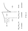
- the band structure of the active region of the starting structure of FIG. 1 is shown in FIG. 2.
- FIG. 2 One can clearly see from this band diagram that there is a quantum well in the boundary region of the Al 0.3 Ga 0.7 As layer 20 and the GaAs layer 18 and that the silicon donor atoms 26 spatially separated from this quantum well serve to place electrons in the quantized energy level within the quantum well. The electrons reach this energy level by tunneling through the Al 0.3 Ga 0.7 As layer 20.
- a line-wise destruction of the starting structure is effected in a vacuum chamber by means of a focused ion beam made of gallium ions (Ga +) with a beam focus of 0.1 ⁇ m, a beam energy of 100 keV and a current density of 10 mA / mm2.
- a focused ion beam made of gallium ions (Ga +) with a beam focus of 0.1 ⁇ m, a beam energy of 100 keV and a current density of 10 mA / mm2.
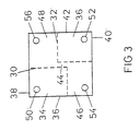
- This creates linear, isolated regions 30, 32, both of which run at right angles in this example and divide the plate with a side length of 100 ⁇ m into a source, a drain, a channel and two gate regions.
- the line-by-line destruction that the lines are the top edges of insulating walls that extend perpendicular to the surface of the initial structure through the entire structure.
- Line 30 thus encloses a closed gate electrode region 34 and line 32 encloses a closed gate electrode region 36.
- these regions are not only surrounded by lines 30 and 32, but also by edge regions 36 and 38 and 40, respectively and 42 of the tile.
- a channel region 44 is defined between the two gate regions and extends from a source region 46 to a drain region 48.
- the regions 34, 36, 46 and 48 are then provided with diffused-in metallic contacts 50, 52, 54 and 56 which represent the external connections of the field effect transistor. Because there is a 2D electron gas in every area is present, which extends over the entire width of the area, voltages applied to the contacted areas are also applied over the entire respective electrode area.
- the field effect transistors are to be kept in the dark according to the invention.
- the width of the conductive channel 44 between the two gate electrode regions is approximately 5 ⁇ m in the present example, in practice even smaller regions are conceivable, even widths below 1 ⁇ m.
- the field effect transistor of FIG. 3 can be operated such that the two gate electrode regions 34 and 36 are coupled to one another by an external conductive connection.
- different gate voltages can also be applied to the gate electrodes, with the advantages also described above.
- FIG. 3 The structure of FIG. 3 can be simplified even further, which is shown in FIG. 4.
- the line 30 is guided in the same way as in the embodiment of FIG. 3, but the line 32 is now designed such that it consists of a first section 58 which extends to the right side of the plate and an angled section 60, which runs parallel to the side 62 of the rectangular gate region.
- the conductive channel 44 is defined here between the angled section 60 and the side 62 of the closed gate electrode region 34.
- This field effect transistor is now only contacted at three points 54, 50 and 56 in order to produce electrical connections to the source, gate and drain.
- the line 32 is also possible to design the line 32 as a simple line, so that the end of the line lies opposite the side or the corner of the connected gate electrode region 34.
- the line which in this case would correspond to line 58, also need not be arranged as shown in FIG. 3, for example it could be drawn from the lower right corner of the plate to just before the corner of the enclosed gate region 34 .
- FIG. 5 shows a diagram 64 of the channel resistance as a function of the gate voltage in the embodiment of FIG. 3.
- both gate electrodes 34 and 36 were connected to one another, so that the same gate voltage at the two Gate electrodes was applied.
- the tips 66 shown do not belong to the measured curve, they were caused by the switching on of other electrical devices.
- the diagram shows an at least essentially straight line 68 which runs from the bottom left to the top right.
- the reciprocal resistance, the channel conductivity, is shown here as a function of the applied gate voltage, the resistance of the leads, in this case 1 kOhm, being taken into account. That is, the straight line shows a value of 1 / (R-1 kOhm).
- the strict linearity of the reciprocal resistance value proves the excellent properties of the field effect transistor.
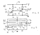
- FIG. 6 shows a conventional circuit diagram of a two-stage amplifier which is formed from two field effect transistors 70 and 72 and two resistors 74 and 76.
- the source 78 of the field effect transistor 70 and the source 80 of the second field effect transistor 72 are connected together at the positive terminal 82.
- the drain 84 of the first field effect transistor 70 is connected via the resistor 74 to the negative terminal 86 and also to the gate electrode 88 of the second field effect transistor 72.
- the drain 90 of the second field effect transistor 72 is applied in a corresponding manner to the negative terminal 86 via the resistor 76.
- a signal to be amplified is applied at the input of the circuit to the gate electrode 92 of the first field effect transistor 70 and the amplified output signal is obtained from the drain 90 of the second field effect transistor 72.
- FIG. 7 shows how this two-stage amplifier can be implemented on a single chip using the method according to the invention.
- the individual reference numerals of the equivalent circuit diagram of FIG. 6 are entered in the drawing of FIG. 7, and FIG. 7 is aligned horizontally with FIG. 6 and has the same scale in the vertical direction.
- Lines in Fig. 6 indicate conductive connections, while in Fig. 7 they symbolize isolating areas.
- the chip has a rectangular shape, and all lines which lie within the lateral boundary of the rectangular chip 94 have been inscribed by a focused ion beam in the manner previously described.
- the area 78, 80 represents a common source area, which is contacted at 82.
- the positive voltage is applied at 82 and distributed to the interconnected source regions 78 and 80 due to the 2D electron gas.
- the negative terminal is located at 86 in the middle of the top field of the chip.
- the input voltage is applied at 92 and the output signal extracted at 90.
- the area 84 represents the drain electrode of the first Field effect transistor 70, the conductive channel 44.1 is defined between the two closely opposing insulating lines between the reference numerals 92 and 84.
- the drain region 84 leads to the left up to the left lateral boundary of the chip, then to the right to the center of the chip, then again to the left and again to the right up to the terminal 86.
- the width of this entire path is designed such that this creates a resistor 74.
- the two closely spaced parallel lines on the right side of the chip lie between the reference symbols 84 and 90 and represent the channel 44.2 of the second field effect transistor 72.
- the drain 90 of the second field effect transistor 72 is also connected to the negative terminal 86 via a meandering path, which represents the resistor 76 and is designed in accordance with the resistor 74 (but mirror-symmetrical to this). Because of these meandering paths, both resistors in this example have inductance.
- the invention proposes a unipolar electronic component with a quasi-one-dimensional carrier channel, which has all the properties of an FET.
- This component is very easy to manufacture, has "self alignment" and linear rather than planar gates with very low capacitance. This enables a very high operating frequency.
- the structure consists of an initially homogeneous 2D layer with high carrier mobility, which is generated by epitaxy on, for example, GaAs. Implantation of accelerated focused ions (eg Ga+ with 100 keV) locally destroys the conductivity of the electron layer. The irradiated areas remain insulating even after illuminating the crystal with bandgap radiation at low or room temperature.
- This inscription of the insulation layer is carried out along two paths (30, 32) on the plate, so that the 2D carrier layer is separated into three areas is divided.
- Source and drain are only connected by a narrow channel (44), the width of which can be continuously adjusted by a gate voltage which is simultaneously applied to the two gate regions (34, 36) with respect to the source, so that there is a large change the carrier concentration and thus the channel resistance.
- the electrical constriction field is parallel to the 2D layer and the destroyed insulating area serves as a dielectric.
- the expansion of the electric field quickly overcomes the destroyed, almost isolated area next to the path affected by the ion beam.
- the carriers are thus limited to a quasi-one-dimensional channel of the initially high-quality plate, and the gate voltage only influences the carrier density, but not the high mobility. This can be very important for ballistic transport, where a large free mean path length is required.
- the current technology of field effect transistors is based exclusively on the "planar" field effect, ie the gate influencing the electronically conductive layer forms a plate capacitor with the former.
- the inhomogeneous stray field at the edges of such gates has only recently been used in basic research to generate quasi-one-dimensional channels.
- the disadvantage of these surface gates is that the inherent capacities are large and thus the maximum working frequencies are limited.
- the production of such laterally delimited layer structures is relatively complicated, especially the sub- ⁇ m-precise positioning of source and drain relative to the gate.
- the IPG transistor presented here does not have these disadvantages and, moreover, can be quickly manufactured in a single technology step without masks and chemical processes. This completely eliminates the positioning problems.
- the basis of the production of the new structure is the laterally local passivation ("isolation letter") of the conductivity of an originally homogeneous electronic layer at the interface of a preferably Al 0.3 Ga 0.7 As - GaAs heterostructure.
- the energy band discontinuity between the Al 0.3 Ga 0.7 As and the GaAs, with suitable doping leads to a band bending in which an electron edge layer is formed just below the crystal surface.
- This electron edge layer is so thin with its thickness of 10 nm (which corresponds approximately to the De Broglie wavelength of the electrons) that quantum effects perpendicular to it become important and one speaks of a two-dimensional electron gas (2DEG).
- Insulation writing in the 2DEG can be done, for example, with a finely focused Ga+ ion beam (Focused Ion Beam, FIB) with 100 keV energy, 100 nm focus diameter. You can "cut" the electrical conductivity of the 2DEG with the ion beam into any area. 8 is applied to a heterostructure in the case of perpendicular ion beam incidence by writing two lines that divide the 2DEG into three areas Gate 1 (36), Gate 2 (34) and the source connected by a very narrow channel 44. Divide drain area 46-48. Since the structure of FIG. 8 corresponds to that of FIG. 3, the same reference numerals have been used for the same parts. The basic structure otherwise completely corresponds to that of FIG. 1.
- FIB finely focused Ga+ ion beam
- a constriction is formed between the source and drain, the effective electrical width ⁇ of which is smaller than the smallest distance ⁇ geo. between the FIB lines.
- the dotted lines 30.1 and 32.1 represent the boundary between the undestroyed crystal structure and the destroyed structure and take into account that the destruction by the ion beam extends beyond the line regions 30, 32 indicated by the bold lines.
- ⁇ By covering the areas of the 2DEG to the right and left of this channel (gate 1 and gate 2) as electrostatic gates with a gate voltage V a relative to the channel (source connection), ⁇ can be tuned from a few ⁇ m to zero.
- the distribution of the electric field E in this structure is shown in FIG. 9. It can clearly be seen that E lies predominantly in the plane of the 2DEG and can therefore pinch off the channel efficiently from both sides.
- the concentric ellipses to the left and right of the quasi-1D channel in the middle indicate the electrical field distribution that is formed due to the applied gate voltage. Due to the small extent of the 2DEG in the direction of crystal growth (approx. 10 nm) and the lateral corners of the gates, an additional field increase (peak effect) occurs near the channel, which further encourages this process. What is special about this structure is not only the simple production of quasi-one-dimensionally conductive channels, but also the method of producing gates from the same conductive structure as the channel, namely from the 2DEG.
- the controlling element "gate” thus has the same structure as the controlled element "channel".
- the capacity can also be estimated at least roughly by theoretical considerations.
- the capacity is 12000. e / 4V ⁇ 0.5 fF, which is in surprisingly good agreement with the value measured above.
- Multiplied by C eff results in a time constant of R g .
- C eff 1 ps, ie this structure can be operated at a frequency of 1 THz.
- R g drops again by about two Orders of magnitude, so that one can expect about 100 THz.
- FIG. 10 corresponds essentially to FIG. 5, but was recorded with a somewhat more sensitive measuring device at a temperature of 1.1 K, namely from a FET with a structure according to FIG. 1 and insulating areas according to FIG. 8.
- the conductivity is in essentially proportional to V g - V th , where V th is the threshold voltage of -4.1V at which the channel is completely cut off (isolating). At low temperatures as in FIG. 10, however, this straight line is superimposed on equidistant structures which occur at integral multiples of the elementary conductivity 2e 2 / h.
- V g -4V the channel is practically isolating.
- the family of curves is symmetrical around the zero point, since
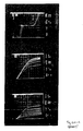
- a) shows the IV characteristic between gate and channel, at -5.6V ⁇ V g ⁇ 5.6V the gates are isolated from the channel.
- b) shows IV characteristic curves for various positive V g , the center of the diagram being the coordinate origin.
- IV characteristics are shown as in b), but for negative V g .
- FIG. 12 shows families of curves of the same IPG structure (ie the structure of FIG. 8, as it was changed for the measurements according to FIG. 11), at room temperature and with larger source-drain voltages V SD of up to 5 V, which are comparable with the applied gate voltages.
- V SD source-drain voltages
- the coordinate origin is in the lower left corner of the Diagram.
- the double lines and light loops are artifacts of the curve recorder.
- This modulation of mobility expresses itself directly in a change in the conductivity of the channel, which is not caused by transhipment processes (speed modulation).
- the response of the IPG transistor is therefore fast and high working frequencies can be achieved.
- the geometry of the IPG arrangement brings about a decisive reduction in the internal capacitances, while a conventional FET represents a capacitance consisting of layers lying on top of one another (gate and 2DEG), the IPG transistor consists of adjacent layers (FIG. 9) which have a gate capacitance which is approximately one order of magnitude lower than in the FET.
- a major strength of the IPG principle according to the invention lies not only in the tunability of the channel conductivity and the broadband nature of the frequency response, but also in the integrability of the structure.
- 6 and 7 have already shown a simple circuit which can be converted directly into an FIB write pattern (FIG. 7).
- the focused ion beam can be processed in one operation, i.e. Without stopping, write IPG transistors, resistors, capacitors and inductors that are ready for use immediately after writing. It is even possible to vary the penetration depth of the ion beam with the ion acceleration voltage and thus selectively structure 2DEG layers lying at different depths laterally, for example in order to produce cross-connections.
- the writing speed of the JIBL-100A ion beam recorder used is a maximum of 0.3 m / s, so that we can already write 106 transistors in 10 s with the available laboratory device - starting from 2 x 2 ⁇ m large IPG transistors!
- FIG. 13A shows a possible configuration of the isolating lines 30, 32 which determine the gate areas.
- a voltage drop occurs along the channel (direction x), which is shown in FIG. 13B.
- V g -V function x
- the "pinch-off” behavior is controlled by using an approximately trapezoidal channel 44 which diverges in the direction of the voltage gradient, ie the channel does not tear off at its end as described above, but becomes narrower uniformly over the entire length. This avoids “hot” areas at the channel end in the case of strongly negative gate voltages near the threshold voltage V th .
- the trapezoidal shape linear processing only achieves a rough comparison measurement of the current density in the channel and other shapes (hyperbola 1 / x, exponential e x , etc.) offer even more favorable effects. All variants lead to a shape that diverges in the direction of the voltage gradient. This model actually only applies to a certain working voltage V o . With deviations from V o , it is less ideal, but still much better than without widening over the length x.
- FIG. 15A shows an example of an OR gate which can be implemented according to the invention, for example as part of a highly integrated circuit.
- the corresponding equivalent circuit diagram is shown in Fig. 15B.
- the lines of the insulating regions are selected such that a channel 100 is formed between two gate regions 101, 102. Below the channel 100 there is a connection area 104 which is connected to a positive terminal of a voltage source. Above the two gate areas 101, 102 is a meandering resistance path 106, which leads from a start 108, which faces the mouth of the channel, to an area 110, which is connected to a negative terminal of the voltage source during operation.
- the area 112 between the channel 100 and the input 108 is contacted at two points 114, 116 and these equivalent contacts, which represent two alternative equivalent output terminals of the OR gate, always carry the same voltage.
- the areas 101, 102, 104 and 110 are provided with corresponding contacts 122, 124, 118 and 120, respectively.
- the side edges of the square chip at the height of the gate regions 101, 102 and at the height of the output region 112 are not shown.
- connection sources in the equivalent circuit diagram are provided with the same reference symbols as in FIG. 15A. All black areas, except for the side edges of the chip, have been made by insulating lettering. If the OR gate has only one component represents a chip, it can be produced, for example, in that the square frame is closed on all sides, except at the points where there is a connection to other components. For this reason, no insulating regions are shown on the sides of the component at the level of the two gate regions 101, 102 and the output region 112. Of course, it is not necessary to contact each of these areas individually when using the component on a chip, since the voltage supply to these areas or the voltage decrease from these areas is generally effected via connections to other components, ie via the two-dimensional charge carrier layer.
- the input region 104 is connected to the output region 110 via the region 106 forming the resistor, so that the channel 100 and the resistor region 106 form a voltage distributor and a corresponding voltage on the contacts 114, 116 can be tapped. Since the resistance of the channel in the open state is very low, the voltage in the drain region 112 corresponds in practice to the source voltage. If, on the other hand, a control voltage is applied to the area 101 and / or to the area 102, this control voltage serves to completely block the channel area 100, so that the voltage in the area 112 corresponds to the voltage prevailing in the area 110.
- the resistance corresponding to the region 106 is also identified with the reference number 106 and the channel 100 is shown with a bold vertical line, which also bears the reference number 100 for easy understanding.
- this bold line 100 or the channel 100 in such a way that it is formed by two FETs whose gate electrodes are connected to one another.
- FIG. 16A shows an AND gate 130
- FIG. 16B shows the equivalent circuit diagram for this AND gate. It can be seen that the design of the AND gate is similar to that of the OR gate, which is why the same reference numerals are used for corresponding areas, but with the addition .1.
- two channel regions 100.1 and 100.2 are provided here, which are each formed between one of the electrode regions 101, 102 and a middle n-shaped insulating line 132.
- the components function as a voltage divider in the conductive state.
- the resistor 106 By a suitable choice of the resistor 106, it is much larger than that of the channel 100 or that of the channels 100.1, 100.2.
- the voltage in the area 112 or in the area 112.1 corresponds to the positive Supply voltage in the range 104 or 104.1, so that a whole series of such gates can be chained in a chip without there being pronounced voltage losses.
- a series of stones i.e. Place insulating areas in a conductive area, such as at 130 in FIG. 15A, which also increases the resistance of that area.
- many more "stones" 130 are required and are placed on the chip in a grid according to FIGS. 17A and 17B instead of the meandering paths.
- logic components can also be easily produced by means of the invention.
- any other known type of gates can also be formed by suitable routing of the insulating regions and such gates can also be combined with one another on a chip in order to produce an integrated or highly integrated circuit, which of course can also be equipped with other active and passive circuit elements. which are also produced using the method according to the invention.
- a mask can be formed by photolithography and then a basic structure according to FIG. 1 can be exposed through the mask by means of an extended ion beam in order to provide a corresponding one to achieve line-by-line destruction.
- the mask can either be a separate thin metal foil which is placed on the surface of the chip, or it can be produced by photolithography on the surface of the chip itself.
- the openings in the mask correspond to the desired insulative lines on the chip in terms of their position and design.
- FIB line a much wider FIB line (line) can be written in order to improve the electrical breakdown behavior at high gate voltages and the total capacity of the gate (s) relative to the source and Decrease drain.
Landscapes
- Engineering & Computer Science (AREA)
- Chemical & Material Sciences (AREA)
- Nanotechnology (AREA)
- Physics & Mathematics (AREA)
- Mathematical Physics (AREA)
- Theoretical Computer Science (AREA)
- Crystallography & Structural Chemistry (AREA)
- Junction Field-Effect Transistors (AREA)
- Element Separation (AREA)
- Internal Circuitry In Semiconductor Integrated Circuit Devices (AREA)
- Semiconductor Integrated Circuits (AREA)
- Insulated Gate Type Field-Effect Transistor (AREA)
Applications Claiming Priority (7)
| Application Number | Priority Date | Filing Date | Title |
|---|---|---|---|
| DE3914007 | 1989-04-27 | ||
| DE3914007 | 1989-04-27 | ||
| DE3942125 | 1989-12-20 | ||
| DE3942125 | 1989-12-20 | ||
| DE3942693 | 1989-12-22 | ||
| DE3942693 | 1989-12-22 | ||
| EP90112970 | 1990-07-06 |
Publications (3)
| Publication Number | Publication Date |
|---|---|
| EP0394757A2 true EP0394757A2 (fr) | 1990-10-31 |
| EP0394757A3 EP0394757A3 (fr) | 1991-07-03 |
| EP0394757B1 EP0394757B1 (fr) | 1998-10-07 |
Family
ID=40139210
Family Applications (2)
| Application Number | Title | Priority Date | Filing Date |
|---|---|---|---|
| EP90106940A Expired - Lifetime EP0394757B1 (fr) | 1989-04-27 | 1990-04-11 | Structure semi-conductrice avec une couche à porteur de charge bidimensionelle et méthode de fabrication |
| EP91111168A Ceased EP0464834A1 (fr) | 1989-04-27 | 1991-07-04 | Méthode de fabrication de structures semi-conductrices actives au moyen de structures de départ ayant une couche bidimensionnelle de porteurs de charge parallèle à la surface |
Family Applications After (1)
| Application Number | Title | Priority Date | Filing Date |
|---|---|---|---|
| EP91111168A Ceased EP0464834A1 (fr) | 1989-04-27 | 1991-07-04 | Méthode de fabrication de structures semi-conductrices actives au moyen de structures de départ ayant une couche bidimensionnelle de porteurs de charge parallèle à la surface |
Country Status (2)
| Country | Link |
|---|---|
| EP (2) | EP0394757B1 (fr) |
| JP (2) | JP2780845B2 (fr) |
Cited By (7)
| Publication number | Priority date | Publication date | Assignee | Title |
|---|---|---|---|---|
| EP0464834A1 (fr) * | 1989-04-27 | 1992-01-08 | Max-Planck-Gesellschaft zur Förderung der Wissenschaften e.V. | Méthode de fabrication de structures semi-conductrices actives au moyen de structures de départ ayant une couche bidimensionnelle de porteurs de charge parallèle à la surface |
| US5338692A (en) * | 1989-04-27 | 1994-08-16 | Max-Planck-Gesellschaft Zur Forderung Der Wissenschaften E.V. | Method of generating active semiconductor structures by means of starting structures which have a 2D charge carrier layer parallel to the surface |
| US5385865A (en) * | 1990-04-26 | 1995-01-31 | Max-Planck-Gesellschaft Zur Forderung Der Wissenschaften | Method of generating active semiconductor structures by means of starting structures which have a 2D charge carrier layer parallel to the surface |
| EP0841704A1 (fr) * | 1996-11-07 | 1998-05-13 | Paul-Drude-Institut für Festkörperelektronik | Dispositif semi-conducteur à transistor et méthode de fabrication |
| WO2014102187A2 (fr) | 2012-12-31 | 2014-07-03 | Technische Universität Ilmenau | Procédé lithographique et dispositif lithographique pour des composants et des circuits ayant des dimensions structurales du domaine micrométrique et nanométrique |
| CN113252762A (zh) * | 2021-04-13 | 2021-08-13 | 西北农林科技大学 | 一种特级初榨橄榄油掺假橄榄果渣油的快速检测方法 |
| CN116995419A (zh) * | 2023-05-18 | 2023-11-03 | 西安电子科技大学 | 用于微波无线传能的发射天线封装结构 |
Families Citing this family (11)
| Publication number | Priority date | Publication date | Assignee | Title |
|---|---|---|---|---|
| GB9206149D0 (en) * | 1992-03-19 | 1992-05-06 | Hitachi Europ Ltd | Charge carrier flow control device |
| JP3182892B2 (ja) * | 1992-07-03 | 2001-07-03 | 松下電器産業株式会社 | 量子素子の製造方法 |
| JPH06244216A (ja) * | 1992-12-21 | 1994-09-02 | Mitsubishi Electric Corp | Ipgトランジスタ及びその製造方法,並びに半導体集積回路装置及びその製造方法 |
| GB9226847D0 (en) * | 1992-12-23 | 1993-02-17 | Hitachi Europ Ltd | Complementary conductive device |
| GB9311111D0 (en) * | 1993-05-28 | 1993-07-14 | Hitachi Europ Ltd | Quantum structure devices |
| US5697428A (en) * | 1993-08-24 | 1997-12-16 | Actronics Kabushiki Kaisha | Tunnel-plate type heat pipe |
| DE19702531B4 (de) * | 1997-01-24 | 2004-04-15 | Fraunhofer-Gesellschaft zur Förderung der angewandten Forschung e.V. | IPG-Transistor mit vertikalem Gate-Komplex und Verfahren zu dessen Herstellung |
| EP1251562A1 (fr) * | 2001-04-20 | 2002-10-23 | Btg International Limited | Dispositifs et circuits nano-électroniques |
| GB0109782D0 (en) * | 2001-04-20 | 2001-06-13 | Btg Int Ltd | Nanoelectronic devices and circuits |
| JP5594780B2 (ja) * | 2011-02-28 | 2014-09-24 | 日本電信電話株式会社 | 半導体回路 |
| JP5814194B2 (ja) * | 2012-07-27 | 2015-11-17 | 日本電信電話株式会社 | 半導体論理回路 |
Family Cites Families (3)
| Publication number | Priority date | Publication date | Assignee | Title |
|---|---|---|---|---|
| US4550330A (en) * | 1984-06-29 | 1985-10-29 | International Business Machines Corporation | Semiconductor interferometer |
| JP2666970B2 (ja) * | 1988-07-18 | 1997-10-22 | 日本電信電話株式会社 | 半導体装置 |
| EP0394757B1 (fr) * | 1989-04-27 | 1998-10-07 | Max-Planck-Gesellschaft zur Förderung der Wissenschaften e.V. | Structure semi-conductrice avec une couche à porteur de charge bidimensionelle et méthode de fabrication |
-
1990
- 1990-04-11 EP EP90106940A patent/EP0394757B1/fr not_active Expired - Lifetime
- 1990-04-27 JP JP2115014A patent/JP2780845B2/ja not_active Expired - Lifetime
-
1991
- 1991-07-04 EP EP91111168A patent/EP0464834A1/fr not_active Ceased
- 1991-07-05 JP JP3190921A patent/JPH05160414A/ja active Pending
Non-Patent Citations (6)
| Title |
|---|
| IEEE TRANSACTIONS ON ELECTRON DEVICES Band ED-29, Nr. 7, Juli 1982, Seiten 1051-1059; D.C. D'AVANZO: "Proton Isolation for GaAs Integrated Circuits" * |
| JAPANESE JOURNAL OF APPLIED PHYSICS Band 29, Nr. 1, Teil 1, Januar 1990, Seiten 48-52, Tokyo, JP; S. NAKATA et al.: "Fabrication of Quantum Wires by Ga Focused-Ion-Beam Implantation and Their Transport Properties" * |
| JOURNAL OF VACUUM SCIENCE & TECHNOLOGY B Band 6, Nr. 3, Mai/Juni 1988, Seiten 1014-1017, New York, US; T. HIRAMOTO et al.: "Fabrication of one-dimensional GaAs wires by focused ion beam implantation" * |
| JOURNAL OF VACUUM SCIENCE & TECHNOLOGY/A Band 4, Nr. 3, Teil 1, Mai/Juni 1986, Seiten 933-938, Woodbury, NY, US; E. MIYAUCHI et al.: "Application of focused ion beam technology to maskless ion implantation in a molecular beam epitaxy grown GaAs or AIGaAs epitaxial layer for three dimensional pattern doping crystal growth" * |
| NUCLEAR INSTRUMENTS & METHODS IN PHYSICS RESEARCH B{nde 209/210, Teil II, Mai 1983, Amsterdam, NL; X.-C. DENG: "Oxygen Ion Beam Modification of GaAs" * |
| PHYSICAL REVIEW B - RAPID COMMUNICATIONS Band 39, Nr. 8, 15. M{rz 1989, Seiten 5535-5537, US; Y. HIRAYAMA et al.: "Electronic transport through very short and narrow channels constricted in GaAs by highly resistive Ga-implanted regions" * |
Cited By (9)
| Publication number | Priority date | Publication date | Assignee | Title |
|---|---|---|---|---|
| EP0464834A1 (fr) * | 1989-04-27 | 1992-01-08 | Max-Planck-Gesellschaft zur Förderung der Wissenschaften e.V. | Méthode de fabrication de structures semi-conductrices actives au moyen de structures de départ ayant une couche bidimensionnelle de porteurs de charge parallèle à la surface |
| US5338692A (en) * | 1989-04-27 | 1994-08-16 | Max-Planck-Gesellschaft Zur Forderung Der Wissenschaften E.V. | Method of generating active semiconductor structures by means of starting structures which have a 2D charge carrier layer parallel to the surface |
| US5396089A (en) * | 1989-04-27 | 1995-03-07 | Max-Planck-Gesellschaft Zur Forderung Der Wissenschaften | Method of generating active semiconductor structures by means of starting structures which have a 2D charge carrier layer parallel to the surface |
| US5385865A (en) * | 1990-04-26 | 1995-01-31 | Max-Planck-Gesellschaft Zur Forderung Der Wissenschaften | Method of generating active semiconductor structures by means of starting structures which have a 2D charge carrier layer parallel to the surface |
| EP0841704A1 (fr) * | 1996-11-07 | 1998-05-13 | Paul-Drude-Institut für Festkörperelektronik | Dispositif semi-conducteur à transistor et méthode de fabrication |
| WO2014102187A2 (fr) | 2012-12-31 | 2014-07-03 | Technische Universität Ilmenau | Procédé lithographique et dispositif lithographique pour des composants et des circuits ayant des dimensions structurales du domaine micrométrique et nanométrique |
| DE102012224537A1 (de) | 2012-12-31 | 2014-07-03 | Technische Universität Ilmenau | Lithographieverfahren und Lithographievorrichtung für Bauteile und Schaltungen mit Strukturabmessungen im Mikro- und Nanobereich |
| CN113252762A (zh) * | 2021-04-13 | 2021-08-13 | 西北农林科技大学 | 一种特级初榨橄榄油掺假橄榄果渣油的快速检测方法 |
| CN116995419A (zh) * | 2023-05-18 | 2023-11-03 | 西安电子科技大学 | 用于微波无线传能的发射天线封装结构 |
Also Published As
| Publication number | Publication date |
|---|---|
| JP2780845B2 (ja) | 1998-07-30 |
| JPH03224244A (ja) | 1991-10-03 |
| EP0394757A3 (fr) | 1991-07-03 |
| JPH05160414A (ja) | 1993-06-25 |
| EP0394757B1 (fr) | 1998-10-07 |
| EP0464834A1 (fr) | 1992-01-08 |
Similar Documents
| Publication | Publication Date | Title |
|---|---|---|
| EP0394757B1 (fr) | Structure semi-conductrice avec une couche à porteur de charge bidimensionelle et méthode de fabrication | |
| DE69332619T2 (de) | Verfahren zur Herstellung von einem Feldeffektbauelement mit einem isolierten Gatter | |
| DE3587485T2 (de) | Flüssigkristall-anzeige-element und dessen herstellung. | |
| DE2611338C3 (de) | Feldeffekttransistor mit sehr kurzer Kanallange | |
| DE69123950T2 (de) | SOI-Feldeffekttransistor und dessen Herstellungsverfahren | |
| DE69518178T2 (de) | Dünnfilmtransistor mit einer Drainversatzzone | |
| DE19522351A1 (de) | Verfahren zur Herstellung von Quantenstrukturen, insbesondere von Quantenpunkten und Tunnelbarrieren sowie Bauelemente mit solchen Quantenstrukturen | |
| EP0033003A2 (fr) | Transistor à effet de champ MOS à double diffusion et procédé pour sa fabrication | |
| EP0011879A1 (fr) | Transistor à effet de champ | |
| DE3686089T2 (de) | Verfahren zur herstellung eines metall-halbleiter-feldeffekttransistors und dadurch hergestellter transistor. | |
| DE2833068C2 (fr) | ||
| DE2727944C2 (fr) | ||
| DE3528562C2 (fr) | ||
| DE3736009C2 (de) | Sperrschicht-FET | |
| US5338692A (en) | Method of generating active semiconductor structures by means of starting structures which have a 2D charge carrier layer parallel to the surface | |
| DE69232767T2 (de) | Quantentöpfe verwendende Quanteneffekt-Halbleiteranordnung zur Ermöglichung kompakter Bauweise und schneller Funktion | |
| DE69219194T2 (de) | Josephsoneffekt-Halbleiteranordnung | |
| EP0675546A2 (fr) | Méthode de fabrication d'un dispositif à électron unique | |
| DE3780620T2 (de) | Halbleiterstruktur mit mehrschichtkontakt. | |
| EP0631322B1 (fr) | Structure de circuit microélectronique et son procédé de fabrication | |
| DE3731000C2 (de) | Integrierte Halbleiteranordnung mit p-Kanal- und n-Kanal-Feldeffekttransistoren | |
| DE69330535T2 (de) | Ladungsträger-Durchflusskontrollanordnung | |
| DE4013662A1 (de) | Verfahren zur erzeugung von aktiven halbleiterstrukturen mittels ausgangsstrukturen mit einer oberflaechenparallelen 2d-ladungstraegerschicht | |
| DE102022211016A1 (de) | Feldeffekttransistor und Verfahren zur Herstellung | |
| DE3942419C2 (fr) |
Legal Events
| Date | Code | Title | Description |
|---|---|---|---|
| PUAI | Public reference made under article 153(3) epc to a published international application that has entered the european phase |
Free format text: ORIGINAL CODE: 0009012 |
|
| AK | Designated contracting states |
Kind code of ref document: A2 Designated state(s): DE FR GB NL |
|
| PUAL | Search report despatched |
Free format text: ORIGINAL CODE: 0009013 |
|
| RHK1 | Main classification (correction) |
Ipc: H01L 21/82 |
|
| AK | Designated contracting states |
Kind code of ref document: A3 Designated state(s): DE FR GB NL |
|
| 17P | Request for examination filed |
Effective date: 19910620 |
|
| 17Q | First examination report despatched |
Effective date: 19940128 |
|
| GRAG | Despatch of communication of intention to grant |
Free format text: ORIGINAL CODE: EPIDOS AGRA |
|
| GRAG | Despatch of communication of intention to grant |
Free format text: ORIGINAL CODE: EPIDOS AGRA |
|
| GRAG | Despatch of communication of intention to grant |
Free format text: ORIGINAL CODE: EPIDOS AGRA |
|
| GRAH | Despatch of communication of intention to grant a patent |
Free format text: ORIGINAL CODE: EPIDOS IGRA |
|
| GRAH | Despatch of communication of intention to grant a patent |
Free format text: ORIGINAL CODE: EPIDOS IGRA |
|
| GRAA | (expected) grant |
Free format text: ORIGINAL CODE: 0009210 |
|
| AK | Designated contracting states |
Kind code of ref document: B1 Designated state(s): DE FR GB NL |
|
| REF | Corresponds to: |
Ref document number: 59010851 Country of ref document: DE Date of ref document: 19981112 |
|
| ET | Fr: translation filed | ||
| GBT | Gb: translation of ep patent filed (gb section 77(6)(a)/1977) |
Effective date: 19981210 |
|
| PG25 | Lapsed in a contracting state [announced via postgrant information from national office to epo] |
Ref country code: GB Free format text: LAPSE BECAUSE OF NON-PAYMENT OF DUE FEES Effective date: 19990411 |
|
| PLBE | No opposition filed within time limit |
Free format text: ORIGINAL CODE: 0009261 |
|
| STAA | Information on the status of an ep patent application or granted ep patent |
Free format text: STATUS: NO OPPOSITION FILED WITHIN TIME LIMIT |
|
| 26N | No opposition filed | ||
| PG25 | Lapsed in a contracting state [announced via postgrant information from national office to epo] |
Ref country code: NL Free format text: LAPSE BECAUSE OF NON-PAYMENT OF DUE FEES Effective date: 19991101 |
|
| GBPC | Gb: european patent ceased through non-payment of renewal fee |
Effective date: 19990411 |
|
| PG25 | Lapsed in a contracting state [announced via postgrant information from national office to epo] |
Ref country code: FR Free format text: LAPSE BECAUSE OF NON-PAYMENT OF DUE FEES Effective date: 19991231 |
|
| NLV4 | Nl: lapsed or anulled due to non-payment of the annual fee |
Effective date: 19991101 |
|
| REG | Reference to a national code |
Ref country code: FR Ref legal event code: ST |
|
| PGFP | Annual fee paid to national office [announced via postgrant information from national office to epo] |
Ref country code: DE Payment date: 20010525 Year of fee payment: 12 |
|
| PG25 | Lapsed in a contracting state [announced via postgrant information from national office to epo] |
Ref country code: DE Free format text: LAPSE BECAUSE OF NON-PAYMENT OF DUE FEES Effective date: 20021101 |