EP0395487A1 - Messvorrichtung, die aus einer Erkennungsschaltung von Strahlung aus einem Träger und einem kalten Finger aus Kryostat besteht - Google Patents
Messvorrichtung, die aus einer Erkennungsschaltung von Strahlung aus einem Träger und einem kalten Finger aus Kryostat besteht Download PDFInfo
- Publication number
- EP0395487A1 EP0395487A1 EP90401096A EP90401096A EP0395487A1 EP 0395487 A1 EP0395487 A1 EP 0395487A1 EP 90401096 A EP90401096 A EP 90401096A EP 90401096 A EP90401096 A EP 90401096A EP 0395487 A1 EP0395487 A1 EP 0395487A1
- Authority
- EP
- European Patent Office
- Prior art keywords
- support
- cover
- detection circuit
- measuring system
- cold finger
- Prior art date
- Legal status (The legal status is an assumption and is not a legal conclusion. Google has not performed a legal analysis and makes no representation as to the accuracy of the status listed.)
- Granted
Links
- 238000001514 detection method Methods 0.000 title claims abstract description 20
- 230000005855 radiation Effects 0.000 title claims abstract description 4
- 229910052751 metal Inorganic materials 0.000 claims abstract description 10
- 239000002184 metal Substances 0.000 claims abstract description 10
- 238000005259 measurement Methods 0.000 abstract description 3
- 239000003292 glue Substances 0.000 abstract 1
- 229910000679 solder Inorganic materials 0.000 abstract 1
- 229910052738 indium Inorganic materials 0.000 description 11
- APFVFJFRJDLVQX-UHFFFAOYSA-N indium atom Chemical compound [In] APFVFJFRJDLVQX-UHFFFAOYSA-N 0.000 description 11
- 238000009736 wetting Methods 0.000 description 6
- 238000000034 method Methods 0.000 description 3
- 238000004026 adhesive bonding Methods 0.000 description 2
- 229910045601 alloy Inorganic materials 0.000 description 2
- 239000000956 alloy Substances 0.000 description 2
- 238000009826 distribution Methods 0.000 description 2
- 238000010438 heat treatment Methods 0.000 description 2
- 238000002844 melting Methods 0.000 description 2
- 230000008018 melting Effects 0.000 description 2
- 229910000978 Pb alloy Inorganic materials 0.000 description 1
- 229910001128 Sn alloy Inorganic materials 0.000 description 1
- 239000011324 bead Substances 0.000 description 1
- 230000005540 biological transmission Effects 0.000 description 1
- 239000011248 coating agent Substances 0.000 description 1
- 238000000576 coating method Methods 0.000 description 1
- 238000001816 cooling Methods 0.000 description 1
- 239000000945 filler Substances 0.000 description 1
- 238000009434 installation Methods 0.000 description 1
- 230000005865 ionizing radiation Effects 0.000 description 1
- 239000000203 mixture Substances 0.000 description 1
- 230000002093 peripheral effect Effects 0.000 description 1
- 238000003825 pressing Methods 0.000 description 1
- 239000000126 substance Substances 0.000 description 1
- 238000003466 welding Methods 0.000 description 1
- 238000004804 winding Methods 0.000 description 1
Images
Classifications
-
- F—MECHANICAL ENGINEERING; LIGHTING; HEATING; WEAPONS; BLASTING
- F25—REFRIGERATION OR COOLING; COMBINED HEATING AND REFRIGERATION SYSTEMS; HEAT PUMP SYSTEMS; MANUFACTURE OR STORAGE OF ICE; LIQUEFACTION SOLIDIFICATION OF GASES
- F25D—REFRIGERATORS; COLD ROOMS; ICE-BOXES; COOLING OR FREEZING APPARATUS NOT OTHERWISE PROVIDED FOR
- F25D19/00—Arrangement or mounting of refrigeration units with respect to devices or objects to be refrigerated, e.g. infrared detectors
- F25D19/006—Thermal coupling structure or interface
-
- G—PHYSICS
- G01—MEASURING; TESTING
- G01J—MEASUREMENT OF INTENSITY, VELOCITY, SPECTRAL CONTENT, POLARISATION, PHASE OR PULSE CHARACTERISTICS OF INFRARED, VISIBLE OR ULTRAVIOLET LIGHT; COLORIMETRY; RADIATION PYROMETRY
- G01J5/00—Radiation pyrometry, e.g. infrared or optical thermometry
- G01J5/02—Constructional details
- G01J5/06—Arrangements for eliminating effects of disturbing radiation; Arrangements for compensating changes in sensitivity
- G01J5/061—Arrangements for eliminating effects of disturbing radiation; Arrangements for compensating changes in sensitivity by controlling the temperature of the apparatus or parts thereof, e.g. using cooling means or thermostats
-
- H—ELECTRICITY
- H10—SEMICONDUCTOR DEVICES; ELECTRIC SOLID-STATE DEVICES NOT OTHERWISE PROVIDED FOR
- H10F—INORGANIC SEMICONDUCTOR DEVICES SENSITIVE TO INFRARED RADIATION, LIGHT, ELECTROMAGNETIC RADIATION OF SHORTER WAVELENGTH OR CORPUSCULAR RADIATION
- H10F77/00—Constructional details of devices covered by this subclass
- H10F77/60—Arrangements for cooling, heating, ventilating or compensating for temperature fluctuations
-
- H—ELECTRICITY
- H10—SEMICONDUCTOR DEVICES; ELECTRIC SOLID-STATE DEVICES NOT OTHERWISE PROVIDED FOR
- H10F—INORGANIC SEMICONDUCTOR DEVICES SENSITIVE TO INFRARED RADIATION, LIGHT, ELECTROMAGNETIC RADIATION OF SHORTER WAVELENGTH OR CORPUSCULAR RADIATION
- H10F77/00—Constructional details of devices covered by this subclass
- H10F77/93—Interconnections
- H10F77/933—Interconnections for devices having potential barriers
Definitions
- the invention relates to a measurement system consisting in particular of a radiation detection circuit, a reading circuit and a support such as a cold cryostat finger.
- the assembly technique known up to now consists of gluing a plate carrying electrical connection tracks to an end face of the cold finger, then gluing the reading circuit to the plate after having soldered it to the detection circuit. by means of metal studs such as indium balls, some of which are also used to ensure the electrical connections between the two circuits.
- the detection circuit is still soldered to the reading circuit by metal studs, but the system also includes a cover fixed to the support and delimiting a cavity with it, the cavity containing the circuits, the cover being provided with electrical conductive tracks, the reading circuit being welded to the cover by metal studs, at least some of which constitute electrical connections and touch the conductive tracks, cover comprising a transparent window in front of which the detection circuit is arranged.
- the support advantageously has a central recess containing the reading circuit and constituting at least partially the cavity, as well as a crown surrounding the recess and notched with radiating grooves opposite the electrical connection tracks.
- the grooves may then contain flexible connectors at the ends of electrical lines, fixed to the support and coming to touch the respective electrical connection tracks.
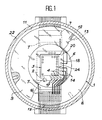
- the cold finger, the reading circuit and the photosensitive detection circuit are designated by the references 1, 2 and 3.
- Indium balls 4 connect by reading the reading circuit 2 and the detection circuit 3 ; some of these balls 4 serve as electrical connections between the two circuits.
- the end of the cold finger 1 is shaped so as to present a peripheral crown 5 surrounding a central hollow 6 and notched with radiating grooves 7, here two in number, between the central hollow 6 and the periphery of the cold finger 1.
- the crown 5 has a flat upper face 8 intended to serve as a support for a cover 9 in the form of a crown, traversed right through by a central window 10, cover 9, the flat lower face 11 of which rests on the upper surface 8 outside the grooves of the cold finger 1.
- Centering lugs 12 stand above the upper surface 8 and fit into corresponding housings 13 established on the cover 9, which can thus be assembled in a position well determined by relation to the cold finger 1.
- Part of the lower face 11 of the cover 9 carries electrical connection tracks 14 distributed in groups so as to come in front of the radiating grooves 7 when the cover 9 and the cold finger 1 are assembled.
- the cold finger 1 carries on its outer surface electrical lines 15 which are fixed to it and which lead to elastic electrical connectors 16 fixed to the bottom of the radiating grooves 7 of the cold finger 1.
- the free end of each connector 16 touches one of the electrical connection tracks 14 and is slightly deformed.
- the metallic connection tracks 14 deviate near the window 10 and lead to respective wetting surfaces 17 which, with other insulated wetting surfaces 18, surround the window 10 on the underside 11.
- wetting surfaces 17 and 18 are intended to allow the adhesion of additional indium balls 19 which also adhere to wetting surfaces of identical distribution established on the face 20 of the integrated circuit 2 which already carries the indium balls 4 for connection to the detection circuit 3.
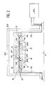
- the reading circuit 2 is in fact contained in the central recess 6, while the detection circuit 3 is without direct contact with the cover 9 and is contained in the window 10.
- the central recess 6 and the window 10 together constitute a cavity which can be closed by placing a filter 21 - optional - on window 10.
- the information coming from the detection circuit 3 is therefore transmitted to the electrical lines 15 by the indium balls 4, the electrical connection tracks 24 installed on the reading circuit 2, the additional indium balls 19, the electrical connection tracks 14 and the connectors 16.
- the entire system is placed in a cryostat where it is protected from the outside environment by a screen 22 provided with a transparent window 23 opposite the detection circuit 3.
- the arrangement of the elements of the measurement system allows easy mounting and space saving since circuits 2 and 3 are housed inside a cavity. Alignment and parallelism of the two circuits 2 and 3 with the cold finger 1 are easily obtained using known techniques such as, for example, that described in international patent application 87 01 509.
- the indium balls 4 and 19 were previously soldered to the reading circuit 2 in a preliminary step of melting then cooling and resolidification. A new melting of the indium balls 4 and 19 causes them to spread over the wetting surfaces of the detection circuit 3 and of the cover 9.
- the weights of these two parts, as well as the surface tension forces prevailing in the molten balls, determine the distances from the detection circuit 3 and the cover 9 to the reading circuit 2. Excellent parallelism can be obtained with appropriate geometrical conditions, in particular if the weight distribution is uniform on the balls 4 and 19.
- the surface tension forces also ensure alignment of the wetting surfaces of the reading circuit 2 with those of the reading circuit 3 and of the cover 9 by horizontally moving these last two parts, as explained in the specification of the aforementioned application.
- the indium beads 4 and 19 are then left to cool until they re-solidify.
- the assembly is completed by coating the upper surface 8 with cold finger 1 and pressing the cover 9 on this upper surface 8 using a press. Excellent parallelism can be obtained between the cover 9 and the upper face 8 of the cold finger 1 since it is possible to press a flat end face of the press on the flat upper surface of the cover 9.
- Bonding can be replaced by welding; the press is then equipped with a winding heating the filler metal.
- the invention can also be implemented in many different ways, with supports such as the cold finger 1 and covers 9 of different shapes, as well as with metal studs of different chemical composition. It is possible to choose the metal of the balls 4 and 19 from indium and its alloys, the lead and tin alloys, the metal or the alloy of the balls 4 which may be different from that of the balls 19.
- the circuit of detection 3 can pick up infrared, ultraviolet, visible light or ionizing radiation in particular.
Landscapes
- Engineering & Computer Science (AREA)
- Physics & Mathematics (AREA)
- Chemical & Material Sciences (AREA)
- Combustion & Propulsion (AREA)
- Mechanical Engineering (AREA)
- Thermal Sciences (AREA)
- General Engineering & Computer Science (AREA)
- General Physics & Mathematics (AREA)
- Spectroscopy & Molecular Physics (AREA)
- Photometry And Measurement Of Optical Pulse Characteristics (AREA)
Applications Claiming Priority (2)
| Application Number | Priority Date | Filing Date | Title |
|---|---|---|---|
| FR8905711 | 1989-04-28 | ||
| FR8905711A FR2646559B1 (fr) | 1989-04-28 | 1989-04-28 | Systeme de mesure constitue d'un circuit de detection d'un rayonnement, d'un circuit de lecture et d'un support tel qu'un doigt froid de cryostat |
Publications (2)
| Publication Number | Publication Date |
|---|---|
| EP0395487A1 true EP0395487A1 (de) | 1990-10-31 |
| EP0395487B1 EP0395487B1 (de) | 1994-07-13 |
Family
ID=9381272
Family Applications (1)
| Application Number | Title | Priority Date | Filing Date |
|---|---|---|---|
| EP90401096A Expired - Lifetime EP0395487B1 (de) | 1989-04-28 | 1990-04-24 | Messvorrichtung, die aus einer Erkennungsschaltung von Strahlung aus einem Träger und einem kalten Finger aus Kryostat besteht |
Country Status (4)
| Country | Link |
|---|---|
| US (1) | US4983840A (de) |
| EP (1) | EP0395487B1 (de) |
| DE (1) | DE69010560T2 (de) |
| FR (1) | FR2646559B1 (de) |
Cited By (3)
| Publication number | Priority date | Publication date | Assignee | Title |
|---|---|---|---|---|
| EP0485312A1 (de) * | 1990-11-09 | 1992-05-13 | Societe Francaise De Detecteurs, Infrarouges- Sofradir | Verfahren zur Herstellung einer übertragbaren Zusammensetzung von einer elektronischen Schaltung für das Lesen und/oder den Betrieb und von einem Leitungsfähigen (oder nicht-)Träger |
| EP0723142A1 (de) * | 1995-01-20 | 1996-07-24 | Societe Francaise De Detecteurs, Infrarouges- Sofradir | Vorrichtung zur Detektion elektromagnetischer Wellen und insbesondere der Infrarotstrahlen |
| WO2013182763A1 (fr) * | 2012-06-08 | 2013-12-12 | Société Française De Détecteurs Infrarouges - Sofradir | Dispositif de détection refroidi avec table froide améliorée |
Families Citing this family (5)
| Publication number | Priority date | Publication date | Assignee | Title |
|---|---|---|---|---|
| FR2651315B1 (fr) * | 1989-08-22 | 1991-11-15 | Detecteurs Infra Rouges Ste Fs | Dispositif de detection infra-rouge. |
| GB2326029A (en) | 1997-06-03 | 1998-12-09 | Marconi Gec Ltd | Cryogenic electronic assembly with stripline connection and adjustment means |
| US5929448A (en) * | 1997-09-03 | 1999-07-27 | The United States Of America As Represented By The Secretary Of The Air Force | Redundant transistor dose monitor circuit using two ICs |
| WO2000042896A2 (en) * | 1999-01-19 | 2000-07-27 | Koninklijke Philips Electronics N.V. | X-ray detector |
| CN105702696B (zh) * | 2016-04-12 | 2019-10-25 | 华天科技(昆山)电子有限公司 | 影像传感芯片的封装结构及其制作方法 |
Citations (4)
| Publication number | Priority date | Publication date | Assignee | Title |
|---|---|---|---|---|
| EP0058645A1 (de) * | 1981-02-09 | 1982-08-25 | SELENIA INDUSTRIE ELETTRONICHE ASSOCIATE S.p.A. | Detektor für infrarote Strahlung |
| EP0136687A2 (de) * | 1983-10-03 | 1985-04-10 | Honeywell Inc. | Infrarotdetektor |
| EP0213421A2 (de) * | 1985-08-07 | 1987-03-11 | Honeywell Inc. | Infrarotdetektoranordnung mit Vakuumkammern |
| WO1987001448A1 (en) * | 1985-09-03 | 1987-03-12 | Santa Barbara Research Center | Integrated infrared detector and cryoengine assembly |
Family Cites Families (9)
| Publication number | Priority date | Publication date | Assignee | Title |
|---|---|---|---|---|
| US3405273A (en) * | 1966-05-02 | 1968-10-08 | Santa Barbara Res Ct | Detector arrangement having a collector with electrically insulating porous material thereon |
| DE2540186C2 (de) * | 1975-09-10 | 1985-03-28 | ANT Nachrichtentechnik GmbH, 7150 Backnang | Anordnung zur Kontaktierung der Massefläche einer Trägerplatte für elektronische Schaltungen |
| JPS59107086A (ja) * | 1982-12-08 | 1984-06-21 | Hitachi Zosen Corp | 貯蔵電力を使用できるハロゲン製造方法 |
| FR2544132B1 (fr) * | 1983-04-08 | 1986-11-21 | Telecommunications Sa | Detecteur photoconducteur en immersion optique |
| JPS60155928A (ja) * | 1984-01-25 | 1985-08-16 | Fujitsu Ltd | 赤外線検知器 |
| JPS61157290U (de) * | 1985-03-22 | 1986-09-29 | ||
| US4766316A (en) * | 1985-08-07 | 1988-08-23 | Honeywell Inc. | Disc detector assembly having vacuum chamber |
| GB8522429D0 (en) * | 1985-09-10 | 1985-10-16 | Plessey Co Plc | Alignment for hybrid device |
| US4728751A (en) * | 1986-10-06 | 1988-03-01 | International Business Machines Corporation | Flexible electrical connection and method of making same |
-
1989
- 1989-04-28 FR FR8905711A patent/FR2646559B1/fr not_active Expired - Lifetime
-
1990
- 1990-04-19 US US07/513,101 patent/US4983840A/en not_active Expired - Fee Related
- 1990-04-24 DE DE69010560T patent/DE69010560T2/de not_active Expired - Fee Related
- 1990-04-24 EP EP90401096A patent/EP0395487B1/de not_active Expired - Lifetime
Patent Citations (4)
| Publication number | Priority date | Publication date | Assignee | Title |
|---|---|---|---|---|
| EP0058645A1 (de) * | 1981-02-09 | 1982-08-25 | SELENIA INDUSTRIE ELETTRONICHE ASSOCIATE S.p.A. | Detektor für infrarote Strahlung |
| EP0136687A2 (de) * | 1983-10-03 | 1985-04-10 | Honeywell Inc. | Infrarotdetektor |
| EP0213421A2 (de) * | 1985-08-07 | 1987-03-11 | Honeywell Inc. | Infrarotdetektoranordnung mit Vakuumkammern |
| WO1987001448A1 (en) * | 1985-09-03 | 1987-03-12 | Santa Barbara Research Center | Integrated infrared detector and cryoengine assembly |
Cited By (7)
| Publication number | Priority date | Publication date | Assignee | Title |
|---|---|---|---|---|
| EP0485312A1 (de) * | 1990-11-09 | 1992-05-13 | Societe Francaise De Detecteurs, Infrarouges- Sofradir | Verfahren zur Herstellung einer übertragbaren Zusammensetzung von einer elektronischen Schaltung für das Lesen und/oder den Betrieb und von einem Leitungsfähigen (oder nicht-)Träger |
| FR2669177A1 (fr) * | 1990-11-09 | 1992-05-15 | Sofradir Ste Fse Detecteurs In | Procede pour realiser l'assemblage reversible d'un circuit electronique de lecture et/ou d'exploitation et d'un support conducteur ou non de l'electricite. |
| US5182852A (en) * | 1990-11-09 | 1993-02-02 | Societe Francaise De Detecteurs Infrarouges (Sofradir) | Reversible production process for assembly of circuit board and substrate |
| EP0723142A1 (de) * | 1995-01-20 | 1996-07-24 | Societe Francaise De Detecteurs, Infrarouges- Sofradir | Vorrichtung zur Detektion elektromagnetischer Wellen und insbesondere der Infrarotstrahlen |
| FR2729757A1 (fr) * | 1995-01-20 | 1996-07-26 | Sofradir | Dispositif de detection d'ondes electromagnetiques, et notamment de rayonnements infra-rouges |
| US5619039A (en) * | 1995-01-20 | 1997-04-08 | Societe Francaise De Detecteurs Infra-Rouges - Sofradir | Device for the detection of electromagnetic waves and, in particular, of infrared radiation |
| WO2013182763A1 (fr) * | 2012-06-08 | 2013-12-12 | Société Française De Détecteurs Infrarouges - Sofradir | Dispositif de détection refroidi avec table froide améliorée |
Also Published As
| Publication number | Publication date |
|---|---|
| US4983840A (en) | 1991-01-08 |
| FR2646559B1 (fr) | 1991-07-05 |
| FR2646559A1 (fr) | 1990-11-02 |
| DE69010560D1 (de) | 1994-08-18 |
| EP0395487B1 (de) | 1994-07-13 |
| DE69010560T2 (de) | 1995-02-09 |
Similar Documents
| Publication | Publication Date | Title |
|---|---|---|
| EP0395487B1 (de) | Messvorrichtung, die aus einer Erkennungsschaltung von Strahlung aus einem Träger und einem kalten Finger aus Kryostat besteht | |
| FR2700416A1 (fr) | Dispositif à semiconducteurs comportant un élément semiconducteur sur un élément de montage. | |
| FR2465335A1 (fr) | Dispositif laser a semi-conducteur | |
| FR2786320A1 (fr) | Batterie a electrolyte non aqueux | |
| EP0766338A1 (de) | Multikontakt für Scheibenantenne | |
| EP0184877A1 (de) | Matrix von elektrolumineszierenden Elementen und deren Herstellungsverfahren | |
| CA2056193C (fr) | Pieces de connexion pour vitrages electrifies | |
| FR2667452A1 (fr) | Connecteur de circuit imprime. | |
| EP0229549B1 (de) | Hermetischer Koaxialsteckverbinder | |
| JP2001111152A (ja) | 半導体レーザ | |
| EP0717442B1 (de) | Träger für integrierten Schaltkreis zur Kontaktierung eines anderen Trägers mittels Kontaktkugeln | |
| FR2698447A1 (fr) | Cellule de mesure micro-usinée. | |
| EP0047195A2 (de) | Kunststoffgehäuse für integrierte Schaltungen | |
| EP0072345B1 (de) | Uhrgehäuse | |
| FR2732509A1 (fr) | Boitier de montage d'une puce de circuit integre | |
| FR2922682A1 (fr) | Procede de fabrication d'un micromodule de capture d'images | |
| EP1278240A2 (de) | Verfahren zur Transferierung von einem Bauelement auf einen Verbindungsträger durch Löten ohne zusätzliches Lötmaterial | |
| FR2794387A1 (fr) | Procede d'assemblage d'un premier element metallique de forme generale cylindrique avec un second element matallique de faible epaisseur, et ensemble rotule et triangle de suspension assembles selon le procede | |
| CA2054912A1 (fr) | Methode de protection de composants electroniques d'un circuit contre les radiations et dispositif utilisant cette methode | |
| EP0983712B1 (de) | Unter 45 grad gebogene elektronische platte | |
| WO2007096515A1 (fr) | Procede d'assemblage d'un boitier comportant des parties metalliques et boitier obtenu | |
| EP0901167A1 (de) | Sockel für eine Leistungsdiode eines Fahrzeugswechselstromgenerators | |
| EP0094869A1 (de) | Verkapselungsgehäuse für mikroelektronische Schaltung mit hoher Wärmeabfuhr, und Verfahren zur Herstellung desselben | |
| FR2498497A1 (fr) | Dispositif pour la coulee continue de metaux | |
| FR2767229A1 (fr) | Capot pour connecteur |
Legal Events
| Date | Code | Title | Description |
|---|---|---|---|
| PUAI | Public reference made under article 153(3) epc to a published international application that has entered the european phase |
Free format text: ORIGINAL CODE: 0009012 |
|
| AK | Designated contracting states |
Kind code of ref document: A1 Designated state(s): DE GB IT |
|
| 17P | Request for examination filed |
Effective date: 19910404 |
|
| 17Q | First examination report despatched |
Effective date: 19930809 |
|
| GRAA | (expected) grant |
Free format text: ORIGINAL CODE: 0009210 |
|
| AK | Designated contracting states |
Kind code of ref document: B1 Designated state(s): DE GB IT |
|
| REF | Corresponds to: |
Ref document number: 69010560 Country of ref document: DE Date of ref document: 19940818 |
|
| ITF | It: translation for a ep patent filed | ||
| GBT | Gb: translation of ep patent filed (gb section 77(6)(a)/1977) |
Effective date: 19940919 |
|
| PLBE | No opposition filed within time limit |
Free format text: ORIGINAL CODE: 0009261 |
|
| STAA | Information on the status of an ep patent application or granted ep patent |
Free format text: STATUS: NO OPPOSITION FILED WITHIN TIME LIMIT |
|
| 26N | No opposition filed | ||
| PGFP | Annual fee paid to national office [announced via postgrant information from national office to epo] |
Ref country code: GB Payment date: 19990415 Year of fee payment: 10 |
|
| PGFP | Annual fee paid to national office [announced via postgrant information from national office to epo] |
Ref country code: DE Payment date: 19990503 Year of fee payment: 10 |
|
| PG25 | Lapsed in a contracting state [announced via postgrant information from national office to epo] |
Ref country code: GB Free format text: LAPSE BECAUSE OF NON-PAYMENT OF DUE FEES Effective date: 20000424 |
|
| GBPC | Gb: european patent ceased through non-payment of renewal fee |
Effective date: 20000424 |
|
| PG25 | Lapsed in a contracting state [announced via postgrant information from national office to epo] |
Ref country code: DE Free format text: LAPSE BECAUSE OF NON-PAYMENT OF DUE FEES Effective date: 20010201 |
|
| PG25 | Lapsed in a contracting state [announced via postgrant information from national office to epo] |
Ref country code: IT Free format text: LAPSE BECAUSE OF NON-PAYMENT OF DUE FEES;WARNING: LAPSES OF ITALIAN PATENTS WITH EFFECTIVE DATE BEFORE 2007 MAY HAVE OCCURRED AT ANY TIME BEFORE 2007. THE CORRECT EFFECTIVE DATE MAY BE DIFFERENT FROM THE ONE RECORDED. Effective date: 20050424 |