EP0396093A2 - Ladungsverschiebeanordnung mit mehreren Registern - Google Patents
Ladungsverschiebeanordnung mit mehreren Registern Download PDFInfo
- Publication number
- EP0396093A2 EP0396093A2 EP90108248A EP90108248A EP0396093A2 EP 0396093 A2 EP0396093 A2 EP 0396093A2 EP 90108248 A EP90108248 A EP 90108248A EP 90108248 A EP90108248 A EP 90108248A EP 0396093 A2 EP0396093 A2 EP 0396093A2
- Authority
- EP
- European Patent Office
- Prior art keywords
- transfer
- registers
- register
- charge
- arrayed
- Prior art date
- Legal status (The legal status is an assumption and is not a legal conclusion. Google has not performed a legal analysis and makes no representation as to the accuracy of the status listed.)
- Granted
Links
Images



Classifications
-
- H—ELECTRICITY
- H10—SEMICONDUCTOR DEVICES; ELECTRIC SOLID-STATE DEVICES NOT OTHERWISE PROVIDED FOR
- H10F—INORGANIC SEMICONDUCTOR DEVICES SENSITIVE TO INFRARED RADIATION, LIGHT, ELECTROMAGNETIC RADIATION OF SHORTER WAVELENGTH OR CORPUSCULAR RADIATION
- H10F39/00—Integrated devices, or assemblies of multiple devices, comprising at least one element covered by group H10F30/00, e.g. radiation detectors comprising photodiode arrays
- H10F39/10—Integrated devices
- H10F39/12—Image sensors
- H10F39/15—Charge-coupled device [CCD] image sensors
- H10F39/156—CCD or CID colour image sensors
Definitions
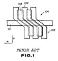
- a region called a register for charge transfer is formed on its chip.
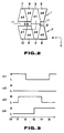
- a transfer electrode for potential control is formed in a side-by-side relation with respect to the register of the charge transfer device, and a channel region operating as the charge transfer route is formed below the transfer electrode.
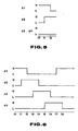
- the signal ⁇ 2 is changed from the "L” level to the "H” level.
- the charges thus far present only in the region of the transfer electrode 31 flow into the region of the transfer electrode 32.
- the signal ⁇ 1 is changed to the "L” level, so that charges continue to be stored only in the lower portion of the transfer electrode 32.
- the present illustrative embodiment is a modification of the first embodiment, in which a first register 81 and a second register 82 for transferring electrical charges in the direction H are provided and the charge transfer may be made across the registers 81, 82 in the direction V.
Landscapes
- Solid State Image Pick-Up Elements (AREA)
- Transforming Light Signals Into Electric Signals (AREA)
Applications Claiming Priority (3)
| Application Number | Priority Date | Filing Date | Title |
|---|---|---|---|
| JP113448/89 | 1989-05-02 | ||
| JP11344889 | 1989-05-02 | ||
| JP11344889 | 1989-05-02 |
Publications (3)
| Publication Number | Publication Date |
|---|---|
| EP0396093A2 true EP0396093A2 (de) | 1990-11-07 |
| EP0396093A3 EP0396093A3 (de) | 1991-09-04 |
| EP0396093B1 EP0396093B1 (de) | 1999-06-23 |
Family
ID=14612490
Family Applications (1)
| Application Number | Title | Priority Date | Filing Date |
|---|---|---|---|
| EP90108248A Expired - Lifetime EP0396093B1 (de) | 1989-05-02 | 1990-04-30 | Ladungsverschiebeanordnung mit mehreren Registern |
Country Status (2)
| Country | Link |
|---|---|
| EP (1) | EP0396093B1 (de) |
| DE (1) | DE69033175T2 (de) |
Cited By (2)
| Publication number | Priority date | Publication date | Assignee | Title |
|---|---|---|---|---|
| EP0504852A1 (de) * | 1991-03-20 | 1992-09-23 | Sony Corporation | Ladungsverschiebeanordnung |
| EP0913869A3 (de) * | 1997-10-29 | 1999-08-18 | Eastman Kodak Company | Aktiver Bildsensor mit programierbarem Farbausgleich |
Family Cites Families (3)
| Publication number | Priority date | Publication date | Assignee | Title |
|---|---|---|---|---|
| US4001878A (en) * | 1975-11-19 | 1977-01-04 | Rca Corporation | Charge transfer color imagers |
| US4513313A (en) * | 1982-12-07 | 1985-04-23 | Canon Kabushiki Kaisha | Solid state imaging device |
| NL8301629A (nl) * | 1983-05-09 | 1984-12-03 | Philips Nv | Halfgeleiderinrichting. |
-
1990
- 1990-04-30 EP EP90108248A patent/EP0396093B1/de not_active Expired - Lifetime
- 1990-04-30 DE DE69033175T patent/DE69033175T2/de not_active Expired - Fee Related
Cited By (3)
| Publication number | Priority date | Publication date | Assignee | Title |
|---|---|---|---|---|
| EP0504852A1 (de) * | 1991-03-20 | 1992-09-23 | Sony Corporation | Ladungsverschiebeanordnung |
| EP0913869A3 (de) * | 1997-10-29 | 1999-08-18 | Eastman Kodak Company | Aktiver Bildsensor mit programierbarem Farbausgleich |
| US6714239B2 (en) | 1997-10-29 | 2004-03-30 | Eastman Kodak Company | Active pixel sensor with programmable color balance |
Also Published As
| Publication number | Publication date |
|---|---|
| EP0396093B1 (de) | 1999-06-23 |
| DE69033175D1 (de) | 1999-07-29 |
| DE69033175T2 (de) | 2000-01-05 |
| EP0396093A3 (de) | 1991-09-04 |
Similar Documents
| Publication | Publication Date | Title |
|---|---|---|
| EP0258001B1 (de) | Festkörperabbildungseinrichtung | |
| JP4338298B2 (ja) | 電荷転送装置およびその駆動方法 | |
| US4513313A (en) | Solid state imaging device | |
| US6885399B1 (en) | Solid state imaging device configured to add separated signal charges | |
| US4750042A (en) | Solid state image pickup element with dual horizontal transfer sections | |
| JP4139088B2 (ja) | 固体撮像装置及びその制御方法 | |
| EP0712238A1 (de) | Festkörper-Bildaufnahmevorrichtung und Ansteuerverfahren dafür | |
| US20040109075A1 (en) | CCD image sensor | |
| EP0593922B1 (de) | Bildaufnahmevorrichtung mit Dual-H-CCD und Verbundkanal | |
| US5317408A (en) | Horizontally aligned image pickup for CCD image sensor | |
| AU607724B2 (en) | Charge-coupled device | |
| EP0396093B1 (de) | Ladungsverschiebeanordnung mit mehreren Registern | |
| US5206530A (en) | Charge transfer device having multiple registers | |
| EP0553869A2 (de) | Verfahren zur Ladungsübertragung, Ladungsübertragungsvorrichtung und Festkörperbildaufnahmevorrichtung zur Anwendung derselben | |
| US5485207A (en) | CCD image sensor for normal and mirror images | |
| US5369434A (en) | Charge transfer device with high speed transfer rate | |
| JP3970425B2 (ja) | 固体撮像装置 | |
| EP0420764B1 (de) | Ladungsverschiebeanordnung mit mäanderförmigem Kanal | |
| US4887160A (en) | Image-pickup device and system capable of outputting either combined (high band) or separate (low band) signals | |
| JP3089507B2 (ja) | 固体撮像素子および信号電荷転送方法 | |
| KR100632334B1 (ko) | 고체 촬상 장치 및 그 구동 방법 | |
| US6207982B1 (en) | Solid-state image pickup device capable of high-speed transfer of signal charges in horizontal direction | |
| JP3153910B2 (ja) | 電荷転送装置 | |
| JPH0685582B2 (ja) | 固体撮像装置 | |
| JPS61294962A (ja) | 一次元カラ−センサ− |
Legal Events
| Date | Code | Title | Description |
|---|---|---|---|
| PUAI | Public reference made under article 153(3) epc to a published international application that has entered the european phase |
Free format text: ORIGINAL CODE: 0009012 |
|
| AK | Designated contracting states |
Kind code of ref document: A2 Designated state(s): DE FR GB |
|
| 17P | Request for examination filed |
Effective date: 19901220 |
|
| PUAL | Search report despatched |
Free format text: ORIGINAL CODE: 0009013 |
|
| AK | Designated contracting states |
Kind code of ref document: A3 Designated state(s): DE FR GB |
|
| 17Q | First examination report despatched |
Effective date: 19950427 |
|
| GRAG | Despatch of communication of intention to grant |
Free format text: ORIGINAL CODE: EPIDOS AGRA |
|
| GRAG | Despatch of communication of intention to grant |
Free format text: ORIGINAL CODE: EPIDOS AGRA |
|
| GRAH | Despatch of communication of intention to grant a patent |
Free format text: ORIGINAL CODE: EPIDOS IGRA |
|
| GRAH | Despatch of communication of intention to grant a patent |
Free format text: ORIGINAL CODE: EPIDOS IGRA |
|
| GRAA | (expected) grant |
Free format text: ORIGINAL CODE: 0009210 |
|
| AK | Designated contracting states |
Kind code of ref document: B1 Designated state(s): DE FR GB |
|
| REF | Corresponds to: |
Ref document number: 69033175 Country of ref document: DE Date of ref document: 19990729 |
|
| ET | Fr: translation filed | ||
| PLBE | No opposition filed within time limit |
Free format text: ORIGINAL CODE: 0009261 |
|
| STAA | Information on the status of an ep patent application or granted ep patent |
Free format text: STATUS: NO OPPOSITION FILED WITHIN TIME LIMIT |
|
| 26N | No opposition filed | ||
| REG | Reference to a national code |
Ref country code: GB Ref legal event code: IF02 |
|
| PGFP | Annual fee paid to national office [announced via postgrant information from national office to epo] |
Ref country code: FR Payment date: 20050408 Year of fee payment: 16 |
|
| PGFP | Annual fee paid to national office [announced via postgrant information from national office to epo] |
Ref country code: GB Payment date: 20050427 Year of fee payment: 16 |
|
| PGFP | Annual fee paid to national office [announced via postgrant information from national office to epo] |
Ref country code: DE Payment date: 20050428 Year of fee payment: 16 |
|
| PG25 | Lapsed in a contracting state [announced via postgrant information from national office to epo] |
Ref country code: GB Free format text: LAPSE BECAUSE OF NON-PAYMENT OF DUE FEES Effective date: 20060430 |
|
| PG25 | Lapsed in a contracting state [announced via postgrant information from national office to epo] |
Ref country code: DE Free format text: LAPSE BECAUSE OF NON-PAYMENT OF DUE FEES Effective date: 20061101 |
|
| GBPC | Gb: european patent ceased through non-payment of renewal fee |
Effective date: 20060430 |
|
| REG | Reference to a national code |
Ref country code: FR Ref legal event code: ST Effective date: 20061230 |
|
| PG25 | Lapsed in a contracting state [announced via postgrant information from national office to epo] |
Ref country code: FR Free format text: LAPSE BECAUSE OF NON-PAYMENT OF DUE FEES Effective date: 20060502 |