EP0396103A2 - Kanalwählendes Gerät - Google Patents
Kanalwählendes Gerät Download PDFInfo
- Publication number
- EP0396103A2 EP0396103A2 EP90108272A EP90108272A EP0396103A2 EP 0396103 A2 EP0396103 A2 EP 0396103A2 EP 90108272 A EP90108272 A EP 90108272A EP 90108272 A EP90108272 A EP 90108272A EP 0396103 A2 EP0396103 A2 EP 0396103A2
- Authority
- EP
- European Patent Office
- Prior art keywords
- channel
- local oscillation
- frequency
- above mentioned
- data corresponding
- Prior art date
- Legal status (The legal status is an assumption and is not a legal conclusion. Google has not performed a legal analysis and makes no representation as to the accuracy of the status listed.)
- Granted
Links
- 230000015654 memory Effects 0.000 claims abstract description 82
- 230000010355 oscillation Effects 0.000 claims abstract description 58
- 230000002401 inhibitory effect Effects 0.000 claims abstract description 10
- 238000001514 detection method Methods 0.000 claims description 3
- 238000010586 diagram Methods 0.000 description 9
- 230000015572 biosynthetic process Effects 0.000 description 8
- 238000000034 method Methods 0.000 description 7
- 239000000969 carrier Substances 0.000 description 3
- 230000007423 decrease Effects 0.000 description 3
- 230000006870 function Effects 0.000 description 3
- 230000004044 response Effects 0.000 description 2
- HDDPSDDDKBZOPX-UHFFFAOYSA-N Abbreviatin PB Natural products CCCC(=O)C1=C(O)C(C)=C(O)C(CC=2C(=C(C(=O)CC)C(O)=C(C)C=2O)O)=C1O HDDPSDDDKBZOPX-UHFFFAOYSA-N 0.000 description 1
- 230000005540 biological transmission Effects 0.000 description 1
- 239000013078 crystal Substances 0.000 description 1
- 230000003247 decreasing effect Effects 0.000 description 1
- 230000005684 electric field Effects 0.000 description 1
- 230000003028 elevating effect Effects 0.000 description 1
- 230000002829 reductive effect Effects 0.000 description 1
- 230000002441 reversible effect Effects 0.000 description 1
- 230000000630 rising effect Effects 0.000 description 1
- 230000035945 sensitivity Effects 0.000 description 1
Images




Classifications
-
- H—ELECTRICITY
- H03—ELECTRONIC CIRCUITRY
- H03J—TUNING RESONANT CIRCUITS; SELECTING RESONANT CIRCUITS
- H03J7/00—Automatic frequency control; Automatic scanning over a band of frequencies
- H03J7/18—Automatic scanning over a band of frequencies
-
- H—ELECTRICITY
- H03—ELECTRONIC CIRCUITRY
- H03J—TUNING RESONANT CIRCUITS; SELECTING RESONANT CIRCUITS
- H03J1/00—Details of adjusting, driving, indicating, or mechanical control arrangements for resonant circuits in general
- H03J1/0008—Details of adjusting, driving, indicating, or mechanical control arrangements for resonant circuits in general using a central processing unit, e.g. a microprocessor
- H03J1/0041—Details of adjusting, driving, indicating, or mechanical control arrangements for resonant circuits in general using a central processing unit, e.g. a microprocessor for frequency synthesis with counters or frequency dividers
- H03J1/005—Details of adjusting, driving, indicating, or mechanical control arrangements for resonant circuits in general using a central processing unit, e.g. a microprocessor for frequency synthesis with counters or frequency dividers in a loop
Definitions
- This invention relates to a channel selecting apparatus to be used for CATV receivers and television receivers.
- the CATV is multi-channeled to diversify the television service.
- a multi-channel CATV system realizing the transmission exceeding 100 channels is operated and a channel selecting system including a tuner so that the receiver may also correspond to it is designed.
- the channel number is continuously sequentially switched. That is to say, the channel number is sequentially made to rise up to a larger number from a smaller number or to fall down reversely to a smaller number from a larger number to select a desired channel. This is called an up/down channel selecting system.
- this up/down channel selecting system in order to elevate the operatability it is generally set to move to the next channel by skipping over a channel not broadcasting at the time of selecting the channel or a channel in which no receiving is desired. That is to say, it is preset to skip the channel.
- the number of the channel desired to be selected is memorized in the address position corresponding to this channel number of a memory (RAM), a region in which the information as to whether this channel is skipped or not is written, that is, a skip flag is set and the skip information of each channel is memorized in the skip flag.
- a total of 181 CH of 1 to 125 CH (CH is an abbreviatin of the channel here and also hereinafter) of the CATV and 14 to 69 CH of the UHF of the TV are made to correspond to position numbers 1 to 181 and are provided respectively with skip flags.
- CH is an abbreviatin of the channel here and also hereinafter
- the case of this example is based on the actual state of the United States of America and 2 to 13 CH of the VHF of the TV and 2 to 13 CH of the CATV are of substantially the same frequency and the same positions.
- the present invention is to eliminate the above mentioned problems and has it as an object to provide channel selecting apparatus wherein the number of skip flags can be made small and the memory (RAM) capacity of the microcomputer can be effectively utilized.
- the present invention is a channel selecting apparatus comprising a tuner whereby a high frequency signal is mixed with a local oscillation signal controlled by a tuning voltage so as to be converted to an intermediate frequency signal to receive a signal of a desired channel and a controlling means whereby data corresponding to a local oscillation frequency are output in each channel on the basis of a channel-up or channel-down channel selecting operation, a tuning voltage is prepared by using these data and the local oscillation frequency of the above mentioned tuner is controlled, wherein the information as to whether the selection of each channel is to be inhibited or permitted at the time of the channel-up or channel-down channel selection is memorized in the above mentioned controlling means and a common channel selection inhibiting information memorizing means is provided for a plurality of channels not allowed to exist simultaneously.
- Fig. 3 is an explanatory view for explaining a skip flag set in the channel selecting apparatus according to the present invention and its memory capacity.
- the skip flags are made common, because, for example, in the United States of America (which shall be mentioned merely as US hereinafter), CATV 2 to 13CH and UHF 2 to 13CH of TV are of the same frequency on the same channel number.
- CATV 65 to 94CH UHF 14 to 43CH of TV and CATV 100 to 125, UHF 44 to 69CH of TV in US, as in, for example, CATV 125CH (of a video carrier frequency of 799.25 MH z ) and UHF 69CH ( of a video carrier frequency of 801.25 MH z )
- the respective channel center frequencies are separated from each other only by 2 MH z
- the signals will be mixed if broadcast simultaneously (that is to say, in the M-NTSC system adopted in US, the sole frequency band of one channel is of 6 MH z , whereas the frequency distance between the above mentioned two channels is only 2 MH z ) and therefore the skip flags are made common. If the skip flags are thus made common between 1 to 125CH of CATV and CH of VHF and UHF of TV, a memory capacity for 56 bits will be able to be saved as compared with the conventional example in Fig. 6.
- the receiving channels are set as fixed to 1 to 1 in response to the position numbers and it is judged by using skip flags whether a skip is made or not
- CATV 2 to 13CH and VHF 2 to 13CH of TV will be made to correspond to the position numbers 2 to 13 and CATV 65 to 94CH
- 100 to 125CH and UHF 14 to 69CH of TV will be made to correspond to the position numbers 65 to 94 and 100 to 125. Therefore, the position numbers may be 1 to 125 corresponding to which skip flags of 125 bits may be provided.
- channel selecting apparatus provided with an AFT (automatic fine tuning) detector
- AFT automatic fine tuning
- the skip flags can be made common in VHF 2 to 13CH and UHF 14 to 69CH of TV and in CATV 2 to 13 and CATV 65 to 94 and 100 to 125CH.
- Fig. 1 is a block diagram showing an embodiment of the channel selecting apparatus according to the present invention.
- the embodiment in Fig. 1 shows a channel selecting apparatus of a frequency synthesizer system.
- this channel selecting apparatus By the way, in the receiver in which this channel selecting apparatus is used, both CATV and TV signals can be received by using the same tuner.
- a TV or CATV high frequency signal (which shall be mentioned as an RF signal hereinafter) is input from an antenna or the like not illustrated.
- This RF signal is fed to a tuner 2 comprising a frequency converter 21 and a voltage controlled oscillator (which shall be mentioned as a VCO hereinafter) 22.
- the frequency converter 21 converts the input RF signal to an intermediate frequency signal (which shall be mentioned as an IF signal hereinafter) by a local oscillation frequency from the VCO 22 which generates a local oscillation frequency fOSC corresponding to a tuning voltage fed from a PLL part 5.
- the above mentioned IF signal is fed to a demodulating circuit 4 through a band pass filter (which shall be mentioned as a BPF hereinafter) 3.
- a TV or CATV demodulating output is obtained from the demodulating circuit 4.
- a central operation processing apparatus (which shall be mentioned as an MPU hereinafter) 6 generates data fOSC* (digital data delivered by the MPU 6 and represented by a local oscillation frequency expression) corresponding to the local oscillatiion frequency for each channel on the basis of the up or down input of the channel (that is, the position) or the CATV/TV switching input from a key input means not illustrated and feeds them to the PLL part 5.
- the MPU 6 will judge whether a skip is to be made or not for each channel with reference to an internal skip flag memory (See Fig. 2) at the up and down time of the channel.
- the MPU 6 has a function of displaying the channel number and displaying being of the CATV at the up and down time of the channel.
- the above mentioned PLL part 5 comprises a programable divider 51, a reference oscillator 52 and a phase detector 53.
- the programable divider 51 is a variable frequency divider dividing the local oscillation frequency fOSC from the VCO 22 by the control signal fOSC* from the MPU 6.
- the reference oscillator 52 is formed of a crystal oscillator and generates a reference oscillation frequency f ref.
- the phase detector 53 compares the phases of the reference oscillation output f ref and the frequency dividing output fo of the programable divider 51 and operates so that, when the phase of fo advances more than f ref, the output will lower.
- This output is a voltage output and is fed to the VCO 22 which is so formed that, when the input voltage increases, the oscillation frequency will increase. Therefore, as a result, the loop of the VCO 22, programable divider 51, reference oscillator 52 and phase detector 53 will become a PLL (phase synchronizing loop).
- PLL phase synchronizing loop
- fOSC operates to be equal to fOSC*. Therefore, if fOSC* is delivered from the MPU 6, the local oscillation frequency fOSC of the VCO 22 will be able to be set at any desired value.
- Fig. 2 is an internal block diagram of the MPU in Fig. 1. This diagram is explained on the case that the CATV/TV switching input is a CATV input.
- the channel up or channel down input is fed to an operation circuit 61 to which are connected a first position memory 62 memorizing 1 position (that is, 1CH) which is the first position of the CATV at the CATV receiving time and a last position memory 63 memorizing 125 position (that is, 125CH) which is the last position of the CATV.
- a first position memory 62 memorizing 1 position (that is, 1CH) which is the first position of the CATV at the CATV receiving time
- a last position memory 63 memorizing 125 position (that is, 125CH) which is the last position of the CATV.
- a channel number memory 64 memorizing channel number data corresponding to the position numbers 1 to 125 of the CATV
- a skip flag memory 65 memorizing the information as to whether a skip is to be made or not at the up/down channel selecting time on the respective channels of the CATV
- a stop position memory 66 to be used to judge (in the step S4 in Fig. 4) whether the skip flag is to be pulled out of the reference loop (closed loop of the steps S2 to S5 in Fig. 4) or not when the information to be skipped is memorized in the skip flag memory 65 corresponding to all the positions.
- the stop position memory 66 the position number, for example, up by 1 from the present position number (in the step S1 in Fig.
- a position number memory 67 memorizing position numbers and an fOSC* memory memorizing data of fOSC* corresponding to the channel numbers.
- a channel to be selected when a channel-up or channel-down input is received, a channel to be selected will be judged without skipping with reference to the skip flag memory 65, the judged selected channel will be memorized in the position number memory 67, data corresponding to this channel will be read out of the channel number memory 64, data fOSC* corresponding to the local oscillation frequency corresponding to the channel number will be prepared with reference to the fOSC* memory and will be output to the PLL part 5 and the channel number display data will be output.
- Fig. 4 shows an example of a key operating part (remote controlled hand unit) to be used to feed a CH-up input, CH-down input and CATV/TV switching input to the MPU 6.
- This key operating part is provided with not only a power source key (POWER) switching on/off the power source of the receiver, CATV/TV key switching the CATV/TV, up-channel selecting key (CHANNEL UP) for the CH-up channel selection and down-channel selecting key (CHANNEL DOWN) for the CH-down channel selection but also ten keys 0 to 9 to be used for the direct channel selection or the like by inputting the channel number into the key and further presetting keys (MEMORY, ADD, ERASE) for memorizing in the skip flag memory 65 the information as to whether skipped or not at the time of up/down-selecting the respective channels of the CATV (or TV).
- POWER power source key
- CATV/TV key switching the CATV/TV
- up-channel selecting key CHANNEL UP
- the MEMORY key is an automatically preset auto-key so that, when it is pushed, the respective channels of the CATV (or TV) will be automatically sequentially switched, or so-called searched, the information of selecting the channel in which the signal is present will be memorized (that is to say, the skip-off information will be memorized) and the information of skipping the channel having no signal will be memorized (that is to say, the skip-on information will be memorized).
- the ADD and ERASE keys are manual keys for the user to manually memorize in the skip flag memory 65 whether the respective channels of the CATV (or TV) are to be skipped or not.
- CATV 94CH and UHF 43CH have a skip flag in common and therefore, in case the skip flag is on as described above and then CATV 94CH is switched to the TV reception, the skip flag will be on even on UHF 43CH.
- the information as to whether the respective channels of the VHF and UHF are to be automatically or manually skipped or not will be able to be memorized.
- Fig. 5 is a flow chart showing the operation of the MPU when channels are up-selected in the CATV.
- the position number will be increased by 1 whenever the key is pushed.
- an operation of making the position number the first position will be made.
- this operation will be made in the operation circuit 61 by referring to the first position memory 62 and last position memory 63.
- the step S4 is a step wherein, when the skip flag 1 stands in all the positions, it will be judged whether the skip flag will be pulled out of the reference loop or not.
- step S5 in the process in which the position number is up, the value of the skip flag corresponding to the value of the position number memory 67 is judged. If the skip flag is on (that is, 1), the program will return to the step S2 and the position number will be automatically skipped to the next number. In the step S5, if the skip flag is off (that is, 0), as shown in the steps S6, S7 and S8 the value of the data fOSC* corresponding to the local oscillation frequency corresponding to the position number then will be determined and output and the respective data of the CATV display and channel number display will be output.
- the operations of the steps S5, S6 and S7 are as explained in Fig. 2.
- a skip flag will be used in common and therefore the number of skip flags can be small. Therefore, the memory (RAM) capacity of the channel selecting microcomputer can be effectively utilized.
- an IFAGC amplifying circuit 7 and size judging circuit 8 are provided between the BPF 3 and MPU 6 in Fig. 6.
- the size judging circuit is a so-called AFT circuit.
- the frequency dividing ratio of the programable divider 51 is set by the data fOSC* from the MPU 6 in which, when the channel to be selected is designated by the user, the frequency dividing ratio will be renewed sequentially at a predetermined period from a frequency dividing ratio so that the frequency (tuned frequency fTUNE) of the local oscillation signal may be sequentially switched within a fixed range (tuned frequency range) from a tuned frequency (which shall be mentioned as a search starting frequency hereinafter) and may be continuously searched.
- the renewal of the frequency dividing ratio of the above mentioned programable divider 51 is controlled according to the size relation between the input signal frequency fIN and search starting tuning frequency fS. That is to say, the IF signal output from the BPF 3 is amplified and controlled to be of a fixed amplitude by the IFAGC amplifying circuit 7. This amplified controlled output is fed to the size judging circuit 8.
- the frequency fIF of the IF signal fed to this size judging circuit 8 will be different from the inherent intermediate frequency f01 in case the input signal frequency fIN is different from the prescribed frequency.
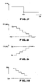
- the size judging circuit 8 judges the sizes of this inherent intermediate frequency f01 and the actual intermediate frequency fIF at the time of starting the search to judge the size relation between the input signal frequency fIN and search starting tuned frequency fS.In this case, as shown in Fig. 7, in case the actual intermediate frequency fIN at the time of starting the search, that is, the search starting tuned frequency fS is larger than the input signal frequency fIN, the size judging circuit 8 will output a high level judging signal VDP. On the other hand, in the case reverse to this, a low level judging signal VDP will be output.
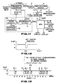
- the search starting tuned frequency fS will be larger than the input signal frequency fIN and therefore, as shown in Fig. 8, the above mentioned MPU 6 wil renew the frequency dividing ratio of the programable divider 51 in the direction of lowering the tuned frequency fTUNE.
- the search starting tuned frequency fS will be smaller than the input signal frequency fIN and therefore, as shown in Fig. 9, the frequency dividing ratio of the programable divider 51 will be renewed in the direction of elevating the tuned frequency fTUNE.
- Fig. 10 shows the case that the search starting tuned frequency fS is larger than the input signal frequency fIN.
- the channel selecting apparatus provided with such AFT circuit as in this embodiment can be applied also to the case that the input signal frequency fIN is offset from the prescribed frequency, for example, as in the HRC (Harmonic Related Carriers) and IRC (Incremental Related Carriers) of the CATV in US.
- HRC Harmonic Related Carriers
- IRC Intelligent Related Carriers
- the apparatus shown in Fig. 11 is considered as another example of an apparatus wherein, in the apparatus shown in Fig. 1, in the case of selecting an object channel by the up/down channel selection, even if the input signal frequency of the channel is different from the normal frequency, it will be automatically searched and the skip information will be able to be memorized in the skip flag memory.
- an AFT detector 9 is provided between the BPF 3 and MPU 6 in Fig. 1.
- the frequency variation of the IF signal from the BPF 3 is taken out as a direct current voltage variation and whether the IF frequency is higher or lower than a predetermined value is transmitted to the MPU 6. That is to say, the AFT detector 9 outputs an AFT voltage VAFT and the MPU 6 controls fOSC* (local oscillation frequency expressing data delivered by the MPU) and searches a frequency f02 in which the VAFT will vary to be on a logical level "0" (0V) from a logical level "1" (5V) when fOSC* is elevated.
- fOSC* local oscillation frequency expressing data delivered by the MPU
- Fig. 13 shows detection characteristics of an AFT detector 9 for an actual television signal.
- Fig. 13 shows variations of VAFT against the variations of fOSC* P
- C and S represent lead-in positions of the AFT repectively by the video carrier, color sub-carrier and sound carrier of the desired channel.
- S-1 and C-1 represent lead-in positions respectively by the sound carrier and color sub-carrier of the lower adjacent channel.
- P+1 represents a lead-in position by the video carrier of the upper adjacent channel.
- the downward directed and upward directed arrows represent respectively the directions of the variation of VAFT when fOSC* is increased.
- the VAFT varies upward. That is to say, it is shown that the rising position fluctuates substantially within this hatched range.
- the downward variation is in only the position in which each carrier is present. The AFT is led into this position.
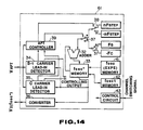
- the operation circuit 61 within the MPU 6 is formed as shown in Fig. 14 so that the normal reception may be possible. That is to say, in the process of searching the frequency f02 corresponding to the video carrier P, it is detected whether the AFT is led into the objective video carrier P, into the sound carrier S-1 of the lower adjacent channel or into the color sub-carrier C and, in case it is led into the carrier S-1 or carrier C, the video carrier P will be searched again.
- Fs and -Fc represent means whereby in order to search the carrier P again at the time of detecting respectively the carrier S-1 and carrier C, data of a fixed frequency to be increased or decreased from the value of fOSC* then are generated so that, at the time of detecting the carrier S-1 or carrier C, the FS or -FC may be switched by a switching circuit 31 and the fixed frequency FS or -FC may be fed to an adder 32 at one input end.
- the value fOSC1 of fOSC* set at the fOSC* memory 33 then is fed to the adder 32 at the other input end.
- the above mentioned 250 KH z is a value taking into consideration the above described fluctuation of 125 KH z of the frequency difference between the channels and the fluctuation of the AFT circuit.
- the value of FC may be about 3.31 MH z in the M-NTSC system.
- 3.31 MH z (Color sub-carrier frequency of 3.579545 MH z ) - 250 KH z .
- a controlling circuit 43 loads an fOSC* memory 33 from an fOSC (EXPE) memory 41 with fixed frequency data corresponding to a desired channel.
- the frequency data fOSC* are converted to a voltage value V2 (fOSC*) by a converter 36 to switch the channel.
- An AFT detector 4 outputs an AFT voltage VAFT corresponding to V2 (fOSC*).
- An AFT controller 39 operates an AFT loop to search f02. When the AFT is led in, the AFT controller 39 will switch the switching circuit 37 to the b side so that an S-1 carrier lead-in detector 34 and carrier lead-in detector 35 may function.
- Whether the AFT is detected by the S-1 carrier lead-in detector 34 or by the C carrier lead-in detector 35 depends on whether the value of fOSC* then is on the sound carrier S-1 side of the lower adjacent channel of each channel or on the color sub-carrier C side of each channel.
- the S-1 carrier lead-in detector 34 switches the switching circuit 31 to a data generating means FS with its controlling output, stores the value of the fOSC* memory 33 then once in an fOSC1 memory 42 and then increases the value of the fOSC* memory 33 by the predetermined frequency FS. Then, the AFT is measured and, when the VAFT is "0", the carrier P will have been detected and therefore the AFT will be judged to have been led into the carrier S-1 at fOSC. In this case, if the carrier is searched again from the value of the fOSC* memory 33 then, that is, fOSC1 + FS, the AFT will be able to be led into the P carrier.
- the switching circuit 37 is switched to the a side to make a search with F STEP data.
- the operation of the switching circuit 38 switching the data memories nF STEP and -nF STEP is the same as in the switching circuit 25 of the prior art example (Fig. 10). If VAFT "0" is not detected in fOSC1 + FS, fOSC1 will be judged to be a carrier P and the value of the fOSC1 memory 32 will be returned to the fOSC* memory 33.
- the C carrier lead-in detector 35 switches the switching circuit 31 to the data generating means -FC with its controlling output, transfers the value of the fOSC* memory 33 then to fOSC1 decreases the value of fOSC* by the predetermined frequency FC. Then the AFT is measured and, when the VAFT is "0", the carrier P will have been detected and therefore the AFT will be judged to have been led into the carrier C at the value fOSC1 of fOSC*. The same as in the case of S-1, if the switching circuit 37 is switched to the a side and the carrier P is searched by the F STEP unit from the carrier fOSC1-FC, the AFT will be able to be led into the carrier P. If VAFT "0" is not detected in fOSC1-FC, fOSC1 will be considered to have been the carrier P and fOSC* will be returned to fOSC1.
- Fig. 15 is to explain an example of the operation of the circuit in Fig. 14. Time is taken on the abscissa and fOSC* is taken on the ordinate. At first, the value of fOSC* is made fOSC1-FC to detect a carrier C. Then, the value of fOSC* is made fOSC1 + FS to detect a carrier S-1. In this case, as the AFT is not led into the carriers C and S-1, the value of fOSC* is returned to fOSC1.
- Fig. 16 is to explain another example of the operation of the circuit in Fig. 14 and shows the case of only detecting the carrier S-1.
- the value of fOSC* is made fOSC1 + FS to detect the carrier S-1.
- the value of fOSC* is returned to fOSC1.
- the frequency differences between S-1 and P and between P and C are utilized and therefore the video carrier P can be discriminated without resorting to a CATV transmitting system (that is, without resorting to the absolute frequency of the video carrier P).
- an automatic channel selection by detecting signals is made possible without causing a mis-operation of selecting channels by leading the AFT into the sound carrier of the lower adjacent channel or the color sub-carrier of the desired channel.
- the detecting characteristics of the AFT detector 9 will be as shown in Fig. 13 but, in case there is no broadcast signal in the desired channel, the characteristics of the AFT detector will be as shown in Fig. 17. It is shown that, in this case, when ⁇ fOSC* is 1.5 MHz, the AFT will be led into spurious I.
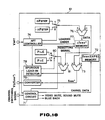
- a controlling circuit 71 feeds fixed frequency data fOSC (EXPE) corresponding to a desired channel to an adder 73 at one input end from an fOSC (EXPE) memory 72.
- EXPE fixed frequency data fOSC
- an AFT voltage (divalent output) VAFT from an AFT detector 9 is input into an AFT controller 74 and is used to switch a switching circuit 75.
- the AFT controller 74 will switch the switching circuit 75 to the data memory nF STEP side in order to increase the frequency at a fixed step F STEP when the VAFT is "1" but will switch the switching circuit 75 to the data memory -nF STEP side in order to decrease the frequency at a fixed step F STEP when the VAFT is "0".
- the output from the switching circuit 75 is fed to an adder 76 at one input end.
- the value of ⁇ fOSC* set in a ⁇ fOSC* memory 77 then is fed to the adder 76 at the other input end.
- the AFT controller 74 detects from the variation of the VAFT that the value of the ⁇ fOSC* memory 77 has become the frequency of the downward directed arrow in Figs.
- FI + ⁇ and FI - ⁇ are means of generating fixed frequency data FI + ⁇ and FI - ⁇ for judging whether the frequency led in by AFT is a spurious frequency FI or not so that, when the AFT leads in the frequency, FI + ⁇ or FI - ⁇ will be switched and the fixed frequency FI + ⁇ or FI - ⁇ will be fed to a subtracter 81 at one input end (+).
- the value of ⁇ fOSC* set at the ⁇ fOSC* memory 77 then is fed to the subtracter 81 at the other input end (-).
- the above mentioned spurious lead-in detector 78 controls the switching circuit 80 to be switched to the a side or b side when the AFT is led in and judges the output of the subtracter 81 to be positive or negative so that, in case the switching circuit 80 is positive when on the a side and is negative when on the b side, the AFT will be considered to be led into the spurious I and this will be transmitted to the controlling circuit 71.
- the controlling circuit 71 will reset the ⁇ fOSC* memory 77 to make the fOSC* output fOSC (EXPE).
- the controlling circuit 71 will judge this channel to be of no signal so that, at the time of an up/down channel selection, that channel will not be selected but the next channel will be selected or, at the time of a direct channel selection, the picture will be made, for example, blue (called a blue back) and the sound will be muted.
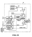
- the controlling circuit 91 delivers frequency data fOSC (EXPE) corresponding to the desired channel to an adder 93 at one input end from an fOSC (EXPE) memory 92.
- EXPE frequency data fOSC
- an AFT voltage (divalent output) VAFT from an AFT detector 9 is input into a P carrier lead-in detector 94 and is used to switch a switching circuit 95.
- the P carrier lead-in detector 94 will switch the switching circuit 95 so as to feed data FP from a data memory FP to a ⁇ fOSC* memory 96.
- the data FP are about +0.2 MHz (See Figs. 13 and 17).
- the ⁇ fOSC* memory 96 When the AFT is led in, the ⁇ fOSC* memory 96 will receive a loading order through an OR-gate 97 from the P carrier lead-in detector 94 and will be loaded with the data FP.
- the P carrier lead-in detector 94 After the above mentioned fOSC* is delivered through a converter 98, after a predetermined time, the AFT voltage VAFT is measured and, when it is 0V, that is, "0" in FP as in Fig. 13, a video carrier P will be recongized to be present and the control will be transferred to an AFT controller 99. At this time, the switch circuit 95 is switched to the a side. By the way, the converter 98 is to convert digital data fOSC* to an analogue voltage value V2 (fOSC*).
- the video carrier P of the desired channel will be judged to be absent and this will be transmitted to the controlling circuit 91.
- the ⁇ fOSC* memory 96 is reset and the fOSC* output is made fOSC (EXPE).
- the controlling circuit 71 will operate the same as in the case of Fig. 18 and, at the time of an up/down channel selection, that channel will not be selected but the next channel will be selected or, at the time of a direct channel selection, the picture will be made, for example, blue (called a blue back) and the sound will be muted.
- the AFT detector 9 will output an AFT voltage VAFT corresponding to V2 (fOSC*) and the AFT controller 99 will operate an AFT loop to search f02. That is to say, the AFT voltage (divalent output) from the AFT detector 9 will be input into the AFT controller 99 and will be used to switch a switching circuit 100.
- the switch circuit 100 is switched to the data memory nF STEP side in order to increase the frequency at a fixed step F STEP when the VAFT is "1" but to the data memory -nF STEP side in order to decrease the frequency at a fixed step F STEP when the VAFT is "0".
- the output from the switch circuit 100 is fed to an adder 101 at one input end.
- the value of ⁇ fOSC* set then at the ⁇ fOSC* memory 96 is fed to the adder 101 at the other input end.
- the output of the adder 93 is output as V2 (fOSC*) through the converter 98.
- the AFT detector 9 outputs an AFT voltage VAFT corresponding to V2 (fOSC*).
- the present invention is useful for automatically selecting channels by detecting present signals and for making a black picture when there is no signal.
Landscapes
- Engineering & Computer Science (AREA)
- Computer Hardware Design (AREA)
- Microelectronics & Electronic Packaging (AREA)
- Channel Selection Circuits, Automatic Tuning Circuits (AREA)
- Television Receiver Circuits (AREA)
Applications Claiming Priority (2)
| Application Number | Priority Date | Filing Date | Title |
|---|---|---|---|
| JP112894/89 | 1989-05-01 | ||
| JP1112894A JP2772032B2 (ja) | 1989-05-01 | 1989-05-01 | 選局装置 |
Publications (3)
| Publication Number | Publication Date |
|---|---|
| EP0396103A2 true EP0396103A2 (de) | 1990-11-07 |
| EP0396103A3 EP0396103A3 (de) | 1991-06-12 |
| EP0396103B1 EP0396103B1 (de) | 1996-04-03 |
Family
ID=14598170
Family Applications (1)
| Application Number | Title | Priority Date | Filing Date |
|---|---|---|---|
| EP90108272A Expired - Lifetime EP0396103B1 (de) | 1989-05-01 | 1990-04-30 | Kanalwählendes Gerät |
Country Status (4)
| Country | Link |
|---|---|
| EP (1) | EP0396103B1 (de) |
| JP (1) | JP2772032B2 (de) |
| KR (1) | KR950003144B1 (de) |
| DE (2) | DE396103T1 (de) |
Cited By (3)
| Publication number | Priority date | Publication date | Assignee | Title |
|---|---|---|---|---|
| WO1996023354A1 (en) * | 1995-01-23 | 1996-08-01 | Rca Thomson Licensing Corporation | Wide frequency spectrum television tuner with single local oscillator |
| WO1996037980A1 (en) * | 1995-05-26 | 1996-11-28 | Silvio Della Mattia | Radio that receives the audio from television programs |
| EP1538831A1 (de) * | 2003-12-01 | 2005-06-08 | ORION ELECTRIC CO., Ltd. | Kanalwählermodul |
Families Citing this family (1)
| Publication number | Priority date | Publication date | Assignee | Title |
|---|---|---|---|---|
| JPH04105722U (ja) * | 1991-02-20 | 1992-09-11 | 三洋電機株式会社 | プリセツト式選局装置 |
Family Cites Families (2)
| Publication number | Priority date | Publication date | Assignee | Title |
|---|---|---|---|---|
| US4375651A (en) * | 1981-07-27 | 1983-03-01 | Zenith Radio Corporation | Selective video reception control system |
| US4510623A (en) * | 1982-07-23 | 1985-04-09 | General Electric Company | Television channel lockout |
-
1989
- 1989-05-01 JP JP1112894A patent/JP2772032B2/ja not_active Expired - Lifetime
-
1990
- 1990-04-30 DE DE199090108272T patent/DE396103T1/de active Pending
- 1990-04-30 DE DE69026300T patent/DE69026300T2/de not_active Expired - Fee Related
- 1990-04-30 EP EP90108272A patent/EP0396103B1/de not_active Expired - Lifetime
- 1990-05-01 KR KR1019900006174A patent/KR950003144B1/ko not_active Expired - Fee Related
Cited By (4)
| Publication number | Priority date | Publication date | Assignee | Title |
|---|---|---|---|---|
| WO1996023354A1 (en) * | 1995-01-23 | 1996-08-01 | Rca Thomson Licensing Corporation | Wide frequency spectrum television tuner with single local oscillator |
| US5983088A (en) * | 1995-01-23 | 1999-11-09 | Rca Thomson Licensing Corporation | Wide frequency spectrum television tuner with single local oscillator |
| WO1996037980A1 (en) * | 1995-05-26 | 1996-11-28 | Silvio Della Mattia | Radio that receives the audio from television programs |
| EP1538831A1 (de) * | 2003-12-01 | 2005-06-08 | ORION ELECTRIC CO., Ltd. | Kanalwählermodul |
Also Published As
| Publication number | Publication date |
|---|---|
| KR950003144B1 (ko) | 1995-04-01 |
| KR900019358A (ko) | 1990-12-24 |
| EP0396103B1 (de) | 1996-04-03 |
| DE69026300T2 (de) | 1996-11-14 |
| DE69026300D1 (de) | 1996-05-09 |
| EP0396103A3 (de) | 1991-06-12 |
| JP2772032B2 (ja) | 1998-07-02 |
| DE396103T1 (de) | 1991-11-07 |
| JPH02291713A (ja) | 1990-12-03 |
Similar Documents
| Publication | Publication Date | Title |
|---|---|---|
| US5193005A (en) | Channel selecting apparatus having a channel skip function | |
| US5313282A (en) | Device for controlling power supplied to a satellite broadcast receiver in a television | |
| EP0477753B1 (de) | Eigenschaft des vorherigen Kanales in einem mit mehrfach-RF-Eingängen-Fernsehempfänger | |
| KR960001540B1 (ko) | 텔레비젼 수상기 | |
| US5034819A (en) | Channel selecting apparatus and method used in a television receiving apparatus and capable of memorizing channel data | |
| KR100202340B1 (ko) | 데이타 엔트리 장치 | |
| KR100406985B1 (ko) | 자동선국 중에 선국된 채널을 표시하는 텔레비젼, 및 그의자동선국화면 표시방법 | |
| JPH0467370B2 (de) | ||
| US6400422B1 (en) | Television receiver | |
| EP0396103A2 (de) | Kanalwählendes Gerät | |
| KR0176719B1 (ko) | 안정상태 검출 장치를 갖는 동조 시스템 | |
| JP3969828B2 (ja) | テレビジョン信号受信装置のrfコンバータ出力チャンネル自動設定装置、ビデオチューナ装置及びvtr | |
| KR930010180B1 (ko) | Tv의 자동 채널 절환장치와 그 방법 | |
| JP2570284B2 (ja) | テレビジヨン受像機 | |
| JP3339389B2 (ja) | 映像機器 | |
| KR100688882B1 (ko) | 아날로그/디지털 방송 겸용 영상표시장치의 채널 스캔시간단축 방법 | |
| KR960006828B1 (ko) | 채널자동탐색장치 및 방법 | |
| JP3379696B2 (ja) | テレビジョン受信装置 | |
| KR0164707B1 (ko) | 비디오 카세트 레코더의 자동 채널 설정 장치 및 방법 | |
| KR20030002531A (ko) | 텔레비젼의 채널 선국 방법 및 장치 | |
| KR910003472Y1 (ko) | 방송신호 자동선국 장치 | |
| KR950007721Y1 (ko) | 2튜너를 가지는 tvcr의 개선된 채널 서치 튜닝 시스템 | |
| KR950013628B1 (ko) | 채널 업/다운시 메모리된 채널 표시 방법 | |
| KR19980058810A (ko) | 영상 기기의 채널 선국 방법 | |
| JPH10136278A (ja) | 選局装置 |
Legal Events
| Date | Code | Title | Description |
|---|---|---|---|
| PUAI | Public reference made under article 153(3) epc to a published international application that has entered the european phase |
Free format text: ORIGINAL CODE: 0009012 |
|
| 17P | Request for examination filed |
Effective date: 19900430 |
|
| AK | Designated contracting states |
Kind code of ref document: A2 Designated state(s): DE FR GB |
|
| PUAL | Search report despatched |
Free format text: ORIGINAL CODE: 0009013 |
|
| AK | Designated contracting states |
Kind code of ref document: A3 Designated state(s): DE FR GB |
|
| EL | Fr: translation of claims filed | ||
| DET | De: translation of patent claims | ||
| 17Q | First examination report despatched |
Effective date: 19940127 |
|
| GRAA | (expected) grant |
Free format text: ORIGINAL CODE: 0009210 |
|
| AK | Designated contracting states |
Kind code of ref document: B1 Designated state(s): DE FR GB |
|
| REF | Corresponds to: |
Ref document number: 69026300 Country of ref document: DE Date of ref document: 19960509 |
|
| ET | Fr: translation filed | ||
| GRAH | Despatch of communication of intention to grant a patent |
Free format text: ORIGINAL CODE: EPIDOS IGRA |
|
| PLBE | No opposition filed within time limit |
Free format text: ORIGINAL CODE: 0009261 |
|
| STAA | Information on the status of an ep patent application or granted ep patent |
Free format text: STATUS: NO OPPOSITION FILED WITHIN TIME LIMIT |
|
| 26N | No opposition filed | ||
| PGFP | Annual fee paid to national office [announced via postgrant information from national office to epo] |
Ref country code: FR Payment date: 19970409 Year of fee payment: 8 |
|
| PGFP | Annual fee paid to national office [announced via postgrant information from national office to epo] |
Ref country code: GB Payment date: 19970421 Year of fee payment: 8 |
|
| PGFP | Annual fee paid to national office [announced via postgrant information from national office to epo] |
Ref country code: DE Payment date: 19970509 Year of fee payment: 8 |
|
| PG25 | Lapsed in a contracting state [announced via postgrant information from national office to epo] |
Ref country code: GB Free format text: LAPSE BECAUSE OF NON-PAYMENT OF DUE FEES Effective date: 19980430 Ref country code: FR Free format text: THE PATENT HAS BEEN ANNULLED BY A DECISION OF A NATIONAL AUTHORITY Effective date: 19980430 |
|
| GBPC | Gb: european patent ceased through non-payment of renewal fee |
Effective date: 19980430 |
|
| PG25 | Lapsed in a contracting state [announced via postgrant information from national office to epo] |
Ref country code: DE Free format text: LAPSE BECAUSE OF NON-PAYMENT OF DUE FEES Effective date: 19990202 |
|
| REG | Reference to a national code |
Ref country code: FR Ref legal event code: ST |