EP0397369A2 - Dispositif optique pour combiner des réseaux lumineux de longueurs d'ondes différentes - Google Patents
Dispositif optique pour combiner des réseaux lumineux de longueurs d'ondes différentes Download PDFInfo
- Publication number
- EP0397369A2 EP0397369A2 EP90304726A EP90304726A EP0397369A2 EP 0397369 A2 EP0397369 A2 EP 0397369A2 EP 90304726 A EP90304726 A EP 90304726A EP 90304726 A EP90304726 A EP 90304726A EP 0397369 A2 EP0397369 A2 EP 0397369A2
- Authority
- EP
- European Patent Office
- Prior art keywords
- beams
- face
- quarter
- mirror
- wave plate
- Prior art date
- Legal status (The legal status is an assumption and is not a legal conclusion. Google has not performed a legal analysis and makes no representation as to the accuracy of the status listed.)
- Granted
Links
- 230000003287 optical effect Effects 0.000 title claims abstract description 114
- 238000003491 array Methods 0.000 title abstract description 69
- 230000010287 polarization Effects 0.000 claims abstract description 155
- 230000001419 dependent effect Effects 0.000 abstract description 17
- 238000006243 chemical reaction Methods 0.000 abstract description 8
- 238000010586 diagram Methods 0.000 description 73
- 230000000694 effects Effects 0.000 description 27
- 230000015654 memory Effects 0.000 description 26
- 238000012545 processing Methods 0.000 description 24
- 230000006870 function Effects 0.000 description 23
- 239000000835 fiber Substances 0.000 description 18
- 238000013507 mapping Methods 0.000 description 14
- 230000005540 biological transmission Effects 0.000 description 12
- 239000000872 buffer Substances 0.000 description 12
- 230000009466 transformation Effects 0.000 description 11
- 238000000844 transformation Methods 0.000 description 10
- 230000000903 blocking effect Effects 0.000 description 9
- 238000000034 method Methods 0.000 description 9
- 238000013461 design Methods 0.000 description 8
- 238000013459 approach Methods 0.000 description 7
- 230000014509 gene expression Effects 0.000 description 6
- 230000004044 response Effects 0.000 description 6
- 238000003384 imaging method Methods 0.000 description 4
- 230000008859 change Effects 0.000 description 3
- 238000004891 communication Methods 0.000 description 3
- 230000009977 dual effect Effects 0.000 description 3
- 239000011159 matrix material Substances 0.000 description 3
- WYTGDNHDOZPMIW-RCBQFDQVSA-N alstonine Natural products C1=CC2=C3C=CC=CC3=NC2=C2N1C[C@H]1[C@H](C)OC=C(C(=O)OC)[C@H]1C2 WYTGDNHDOZPMIW-RCBQFDQVSA-N 0.000 description 2
- 230000004075 alteration Effects 0.000 description 2
- 230000000295 complement effect Effects 0.000 description 2
- 230000003750 conditioning effect Effects 0.000 description 2
- 238000011161 development Methods 0.000 description 2
- 230000018109 developmental process Effects 0.000 description 2
- 238000005192 partition Methods 0.000 description 2
- 210000001747 pupil Anatomy 0.000 description 2
- 229920002319 Poly(methyl acrylate) Polymers 0.000 description 1
- 230000003321 amplification Effects 0.000 description 1
- 230000008901 benefit Effects 0.000 description 1
- 230000001427 coherent effect Effects 0.000 description 1
- 239000012141 concentrate Substances 0.000 description 1
- 230000001143 conditioned effect Effects 0.000 description 1
- 238000012937 correction Methods 0.000 description 1
- 230000007423 decrease Effects 0.000 description 1
- 230000003247 decreasing effect Effects 0.000 description 1
- 230000001934 delay Effects 0.000 description 1
- 238000000605 extraction Methods 0.000 description 1
- 239000004744 fabric Substances 0.000 description 1
- 210000000887 face Anatomy 0.000 description 1
- 239000011521 glass Substances 0.000 description 1
- 230000010354 integration Effects 0.000 description 1
- 238000002372 labelling Methods 0.000 description 1
- 238000004519 manufacturing process Methods 0.000 description 1
- 230000004048 modification Effects 0.000 description 1
- 238000012986 modification Methods 0.000 description 1
- 238000003199 nucleic acid amplification method Methods 0.000 description 1
- 238000012634 optical imaging Methods 0.000 description 1
- 230000008569 process Effects 0.000 description 1
- 201000008752 progressive muscular atrophy Diseases 0.000 description 1
- 230000001902 propagating effect Effects 0.000 description 1
- 230000009467 reduction Effects 0.000 description 1
- 230000008929 regeneration Effects 0.000 description 1
- 238000011069 regeneration method Methods 0.000 description 1
- 230000000717 retained effect Effects 0.000 description 1
- 230000002441 reversible effect Effects 0.000 description 1
- 230000035945 sensitivity Effects 0.000 description 1
- 239000000758 substrate Substances 0.000 description 1
- 108020001572 subunits Proteins 0.000 description 1
- 230000001360 synchronised effect Effects 0.000 description 1
- 239000010409 thin film Substances 0.000 description 1
Images


Classifications
-
- G—PHYSICS
- G02—OPTICS
- G02B—OPTICAL ELEMENTS, SYSTEMS OR APPARATUS
- G02B27/00—Optical systems or apparatus not provided for by any of the groups G02B1/00 - G02B26/00, G02B30/00
- G02B27/28—Optical systems or apparatus not provided for by any of the groups G02B1/00 - G02B26/00, G02B30/00 for polarising
- G02B27/283—Optical systems or apparatus not provided for by any of the groups G02B1/00 - G02B26/00, G02B30/00 for polarising used for beam splitting or combining
Definitions
- the optical devices employed in free space architectures require four or more ports: two signal or data inputs to set the state of each device, a power or clock input to read the state of the device, and a signal or data output comprising a reflected or transmitted power input modulated by the device. If the devices are connected in a switching network, for example, one or more additional ports are required for inputs used to control the switching nodes of the network. To avoid any interference or coherent artifact "noise", the inputs incident on each device may have orthogonal modes with respect to one another. Thus the inputs may differ in polarization, wavelength, time, or spatial location.
- lossless beam combination techniques that divide the aperture, i.e., pupil division, should not be used.
- These beam combination constraints limit the number of signal beams which may be fanned into a device without loss of power or resolution (space-bandwidth product).
- the number of available orthogonal modes also limits the number and type of interconnection operations that can be performed between two arrays of devices, since the use of a mode for signal interconnection directly affects how the signal beams will be combined with the power beam and separated from the output beam.
- an exemplary apparatus for performing wavelength-dependent beam combination which relies on a polarization beam splitter advantageously in combination with other optical elements to develop combined beams with the same polarization type and that are therefore suitable for polarization-dependent combination with other beam arrays.
- a dichroic mirror which is used as the wavelength-dependent element of the apparatus, is oriented such that the incident beams are substantially perpendicular to the mirror. With this orientation, the dichroic mirror achieves near-ideal performance even with beam arrays having a substantial angular field.
- the exemplary apparatus also uses two plates which, although designed for operation as quarter-wave plates at one of the two wavelengths being combined, are oriented with their respective fast axes substantially perpendicular to each other such that polarization conversions, effected by the plates on beams having the other of the two wavelengths, substantially cancel each other.
- An apparatus in accordance with the invention includes means for transmitting first linearly polarized beams in a first direction with a first wavelength and means for transmitting second linearly polarized beams in a second direction with a second wavelength.
- An optical setup including a polarization beam splitter, responds to receipt of the first and second beams in the first and second directions, respectively, by transmitting the first and second beams in the same direction with the same linear polarization type from a surface of the polarization beam splitter.
- the first beams referred to as power beams
- the second beams referred to as control beams
- the power and control beam arrays are received at first and second faces, respectively of the polarization beam splitter, are combined and emerge from a third face of the polarization beam splitter both having p-type polarization.
- the polarization beam splitter is substantially transmissive with respect to light of p-type linear polarization at both 780-nanometer and 850-nanometer wavelengths and is substantially reflective with respect to light of s-type linear polarization at the 850-nanometer wavelength (FIG. 89).
- the power beams are reflected by the polarization beam splitter and the reflected power beams are transmitted to a dichroic mirror where they are reflected back to the polarization beam splitter.
- a quarter-wave plate, designed for 850-nanometer operation, is interposed between the second face of the polarization beam splitter and the dichroic mirror.
- the quarter-wave plate converts the power beams from s-type linear polarization to circular polarization as the power beams are transmitted from the second face to the dichroic mirror and from circular polarization to p-type linear polarization as the power beams are transmitted from the dichroic mirror back to the second face.
- the power beams are transmitted through the polarization beam splitter, emerging from the third face with p-type linear polarization.
- a second quarter-wave plate also designed for 850-nanometer operation, is oriented substantially parallel to the dichroic mirror.
- the second quarter-wave plate has a fast axis that is substantially perpendicular to a fast axis of the first quarter-wave plate.
- the control beams are converted to elliptical polarization as they are transmitted through the second quarter-wave plate, they are transmitted through the dichroic mirror, and they are converted from elliptical polarization back to p-type linear polarization as they are transmitted through the first quarter-wave plate to the second face.
- the control beams then are transmitted through the polarization beam splitter, emerging from the third face with p-type linear polarization.
- the illustrative apparatus of FIG. 90 is then used to perform a further combination of the power and control beam arrays with two 850-nanometer signal beam arrays, the first signal beams having p-type linear polarization and the second signal beams having s-type linear polarization.
- the beam combination is based on space-multiplexing using space-variant mirrors having transmissive areas and reflective areas.
- S-SEEDs symmetric self electro-optic effect devices
- U. S. Patent 4,754,132 issued to H. S. Hinton et al., on June 28, 1988.
- the power beams are selectively reflected from the S-SEEDs and emerge from the apparatus of FIG. 90 as an array of output beams.
- the illustrative apparatus of FIG. 87 which also includes a space-variant mirror, performs a position- dependent combination of a disable beam array, received in one direction, and a preset beam array, received in another direction, to form the control beam array referred to previously.
- FIGS. 98 and 99 Two alternative embodiments of the invention are shown in FIGS. 98 and 99. Both embodiments include a polarization beam splitter and a dichroic mirror and perform wavelength dependent beam combination where the combined beams emerge with s-type linear polarization.
- the polarization beam splitter is substantially transmissive with respect to light of p-type linear polarization at an 850-nanometer wavelength and is substantially reflective with respect to light of s-type linear polarization at both 780-nanometer and 850-nanometer wavelengths.
- FIG. 98 the polarization beam splitter is substantially transmissive with respect to light of p-type linear polarization at an 850-nanometer wavelength and is substantially reflective with respect to light of s-type linear polarization at both 780-nanometer and 850-nanometer wavelengths.
- a further alternative embodiment of the invention shown in FIG. 100 uses the principles of the apparatus of FIG. 88 together with the principles of the apparatus of FIG. 98 to perform a wavelength-dependent combination of four beam arrays where two beam arrays emerge with s-type linear polarization and the other two beam arrays emerge with p-type linear polarization.
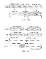
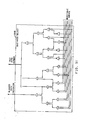
- One specific illustrative embodiment of the invention is used in a beam combination unit 200, part of the exemplary photonic system 10 (FIG. 1) which implements a 16 x 16 circuit-switched, space division switching network.
- Sixteen optical input signals are received on the fibers of a 2 x 8 fiber cable array 21.
- Each optical input signal may be circuit-switched by photonic system 10 for transmission on one fiber of a 2 x 8 fiber cable array 22 as an optical output signal.
- Photonic system 10 includes a lens 80, a data input unit 40, eight optical hardware modules 50 through 57, and a lens 70. It is important to note that photonic system 10 processes arrays of beams in parallel and that the optical transmissions represented by single beams in FIG. 1 are beam arrays of rectangular cross-section.
- the network topology implemented by photonic system 10 comprises expansion, a perfect shuffle equivalent network, and concentration.
- the topology is based on a three-dimensional crossover network 2110 (FIGS. 55-57) having nine node stages NO through N8 and eight link stages LO through L7. Each node stage, for example, stage N2, comprises 32 nodes numbered 0 through 31.
- a 4 x 8 array 500 (FIGS. 1 and 58) of symmetric self electro-optic effect devices (S-SEEDs) corresponds to one node stage of network 2110.
- the S-SEEDs which selectively reflect light depending on their optical state, are the switching nodes of photonic system 10.
- link stages L0, L1, L5, and L6 of network 2110 effect horizontal connections and that link stages L2, L3, L4, and L7 effect vertical connections. Also note that the number of partitions or crosses varies from stage to stage. These variations are implemented in photonic system 10 by variations among the optical hardware modules 50 through 57 as described herein.
- FIG. 2 is a diagram of a system 1600 comprising an expansion (fanout) section 1610, a perfect shuffle equivalent network 1620, and a concentration (fanin) section 1630.
- Perfect shuffle equivalent network 1620 has four node stages 1621-0, 1621-1, 1621-2 and 1621-3 comprising 2x2 nodes, and three link stages 1622-0, 1622-1 and 1622-2 each effecting the same perfect shuffle interconnection of successive node stages.
- System 1600 has more than two paths between each of the N inlets and each of the M outlets.
- Individual nodes of the node stages 1621-0, 1621-1, 1621-2 and 1621-3 are controlled by corresponding stage controllers 1640, 1641, 1642, 1643 in response to instructions from a shuffle network controller 1650.
- expansion section 1610 and concentration section 1630 Three alternative implementations for the expansion section 1610 and concentration section 1630 are shown in FIGS. 3, 4 and 5.
- expansion section 1710 FIG. 3
- Expansion section 1810 FIG. 4
- concentration section 1830 has a single stage 1811 of 1x4 nodes
- concentration section 1830 has a single stage 1831 of 4x1 nodes.
- Expansion section 1910 (FIG. 5) has two stages 1911 and 1912 of lx2 nodes and concentration section 1930 has two stages 1931 and 1932 of 2x1 nodes.
- Each of the expansion sections 1710, 1810, 1910 connects each of the N inlets to multiple inputs of node stage 1621-0 in a perfect shuffle sustaining pattern as defined herein.
- Each of the concentration sections 1730, 1830, 1930 connects multiple outputs of node stage 1621-3 to each of the M outlets in a perfect shuffle sustaining pattern as defined herein.
- FIGS. 6, 7 and 8 Three alternative 2x2 switching nodes 1510, 1520, and 1530 for use in system 1600 are shown in FIGS. 6, 7 and 8.
- a node with n inputs and m outputs is said to be a full capacity node if it is able to convey min ⁇ n,m ⁇ signals at the same time.
- a node is said to be a capacity one node if it is able to convey only one signal at a time.
- a capacity one node may have selectivity of either inputs or outputs or may have no selectivity.
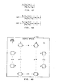
- Node 1510 (FIG. 6), a full capacity node, comprises two selectors 1511 and 1512. Selector 1511 connects either of the node inputs 11 and 12 to node output 01 in response to a selection signal S1. Selector 1512 connects either of the node inputs 11 and 12 to node output 02 in response to a selection signal S2.
- Node 1520 (FIG. 7), a capacity one node with input selectivity, comprises two AND-gates 1521 and 1522, and an OR-gate 1523.
- AND-gate 1521 transmits a signal from input 11, via OR-gate 1523, to both outputs 01 and 02 in response to a selection signal S1.
- AND-gate 1522 transmits a signal from input 12, via OR-gate 1523, to both outputs 01 and 02 in response to a selection signal S2. Only one of the selection signals S1 and S2 is a logic one at any time.
- Node 1530 (FIG. 8), a capacity one node without selectivity, comprises an OR-gate 1531 and an AND-gate 1532.
- AND-gate 1532 transmits the logic union of the signals at the inputs 11 and 12, to both outputs 01 and 02.
- the control signal C is a logic zero
- AND-gate 1532 transmits a logic zero to both outputs 01 and 02. Only one of the inputs 11 and 12 receives an active signal at any time.
- Node 1530 represents a special case of a more general switching node referred to herein as an nxm-module.
- An nxm-module which has n inputs and m outputs, either routes the logical union of the signals at the n inputs to all of the m outputs, or routes none of the signals at the n inputs to any of the m outputs. If a network of nxm-modules is controlled such that at most one input of an nxm-module has an active signal, the nxm-module functions to either route the signal to all of the m outputs or to leave the m outputs idle.
- Node 1530 is a 2x2-module, also referred to herein as a 2-module.
- system 1600 (FIG. 5) is implemented using 2-modules, such as node 1530, as the switching nodes of perfect shuffle equivalent network 1620 as well as in expansion section 1910 and concentration section 1930, the 2-modules of perfect shuffle equivalent network 1620 are individually disabled or enabled as necessary such that none of the 2-modules has more than one active input signal.
- the 2-modules of the last expansion node stage 1912 are also individually disabled or enabled (not shown in FIG. 5) such that a signal received at a given one of the N inlets is transmitted to only two 2-modules of node stage 1621-0.
- all the expansion and concentration 2-modules may be controllable.
- System 1601 is identical to system 1600 (FIG. 2) except that concentration section 1630 is not required.
- System 1602 is identical to system 1600 (FIG. 2) except that expansion section 1610 is not required.
- a single stage strictly nonblocking network 1002 is shown in FIG. 11.
- network 1002 the minimum number of paths between any input-output pair is equal to one. There are no blocked paths because each horizontal rail is uniquely associated with an input and each vertical rail is uniquely associated with an output. Therefore, we have
- a general strictly nonblocking three stage Clos network 1006 is shown in FIG. 13. (The inter-stage links are omitted in FIG. 13.) Applying the strictly nonblocking condition to network 1006, the minimum number of paths between any input-output pair is equal to r. The maximum number of blocked paths is equal to (n-1) + (m-1) and therefore whenever r n + m -1, network 1006 is strictly nonblocking. Note that an S + 2 stage Clos network can be recursively produced from an S stage Clos network by simply replacing each switch in a given stage with a three stage Clos network. A strictly nonblocking five stage Clos network 1008 as shown in FIG. 14 with the number of links between stages indicated thereon. Two problems in implementing Clos networks in the photonic domain are: 1) non-square, non-small switching elements, and 2) different numbers of links between stages (increasing geometrically toward the center).
- a multistage interconnection network (MIN) 1010 is shown in FIG. 15 and is defined by the following five conditions:
- An extended generalized shuffle (EGS) network 1012 is shown in FIG. 16.
- An EGS network is a MIN with a particular specified link interconnection pattern.
- the nodes are numbered consecutively from 0 to r i -1 and the outputs on a particular node are numbered consecutively from 0 to m i -1.
- the outputs of the stage i nodes are then numbered consecutively from 0 to r i m i -1; output o; on node x i is numbered x i m i + o i .
- stage i output x i m i + o i is connected to node (x i m i + o i ) mod r i+1 in stage i + 1.
- This interconnection pattern assigns links consecutively to nodes in the next stage (the so called perfect shuffle).
- An important implication of the EGS interconnection pattern is that the number of paths between any two nodes in two given stages never differs by more than one. For i ⁇ j, the number of paths between a node in stage i and a node in stage j is either where ⁇ x ⁇ denotes the smallest integer ⁇ x and LxJ denotes the largest integer ⁇ x.
- FIGS. 17 and 18 An example EGS network 1014 is shown in FIGS. 17 and 18. To determine the number of paths between input x and output y, we calculate
- the channel graph L(x,y) of input x and output y is the union of all paths between x and y. To ascertain an upperbound on the number of blocked paths, we must determine the number of calls which can intersect any channel graph and also the number of paths that each call can block.
- the channel graph L(x,y) is shown by dark lines in FIG. 19.
- the number of paths between input x and output y blocked by link i of the intersecting call C(i,j) is given by the product of the number of paths from x to the stage i node of C(i,j) and the number of paths from the stage i + 1 node of C(i,j) to y.
- the maximum number of paths from any input (or stage 1 node) to any stage i node is and the maximum number of paths from any stage i + 1 node to any output (or stage S node) is Thus, the maximum number of paths between x and y blocked by link i of C(i,j) is The additional number of paths blocked by link i + 1 is given by
- the second term subtraction corrects for the fact that the first term includes some paths blocked by link i; namely, all those paths reaching link i + 1 via link i. Employing a similar correction for each remaining link of C(i,j) we have that the number of paths blocked by C(i,j) is given by
- the forward-backward invariance property can be stated as follows: every stage j node which can be reached by a given stage i node reaches exactly the same set of stage i nodes.
- the FBIP holds for stages i and j in an EGS network if divides r j .
- the paths between certain stage 3 and stage 5 nodes for network 1014 are shown by dark lines in FIG. 22. Note that every stage 5 node which can be reached by a given stage 3 node reaches exactly the same set of stage 3 nodes.
- the FBIP is important because it drastically reduces intersecting calls and produces multistage modularity.
- An expanding means is said to connect each of the N inlets of G to multiple inputs of the first stage nodes of G in a perfect shuffle sustaining pattern if either of the following two conditions holds.
- a concentrating means is said to connect multiple outputs of the last stage S of nodes of G to each of them outlets of G in a perfect shuffle sustaining pattern if either of the following two conditions holds.
- Network G with such expanding and concentrating means can be equivalently represented as an S + 2 stage perfect shuffle equivalent network comprised of an expansion stage of N 1xF nodes, followed by the S stages of G, followed by a concentration stage of M F x1 nodes.
- ⁇ I ( ⁇ I ) is applied to the N inlet nodes and inlet node ⁇ is connected to node in stage 1 of G according to Condition 1e (2e) and ⁇ 0 ( ⁇ 0 ) is applied to the M outlet nodes and node a in stage S of G is connected to outlet node ⁇ according to Condition 1c (2c).
- Condition 1c 2c
- Crossover network 1020 shown in FIG. 25 is a perfect shuffle equivalent network. This can easily be verified by examining the labeling of the nodes in each stage and the interconnection between stages. The existence of such regularized physical interconnection patterns of perfect shuffle equivalent networks is important for implementation consideration.
- the values selected for the various r i greatly affect the performance and connectivity of the network.
- network 1012 shown in FIG. 16, is an EGS network having an interconnection pattern that simply assigns links consecutively to switches in the next stage--a perfect shuffle interconnection.
- the number of paths P between any inlet x and any outlet y in network 1012 is given by Let I(k) denote the integer set ⁇ 0,1, ⁇ ,k-1 ⁇ . Denote a given path from inlet x to outlet y by the triple (x,P*,y), where P * is an element of I(P). Path (x,P*,y) will pass through stage i switch for 1 ⁇ i ⁇ S. Denote a link between stages i and i + 1 as a stage i link. Path (x,P * ,y) utilizes stage i link for 1 ⁇ i ⁇ S-1.
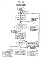
- Processing begins with block 1102 where a previously unchecked path P * is selected.
- the busyiidle status of L i (x,P*, y) is checked for all i, 1 ⁇ i ⁇ S - 1.
- decision block 1106 a determination is made of whether all the L i (x,P*,y) are idle.
- processing proceeds from block 1106 to block 1108 where it is concluded that path P * may be used to connect inlet x to outlet y. If it is determined in block 1106 that all the L i (x,P*,y) are not idle, processing continues with decision block 1110. In block 1110 it is determined whether there are other unchecked paths. If there are, processing returns to block 1102 and the processing flow chart is repeated for a new unchecked path. However, if in decision block 1110 it is determined that there are no other unchecked paths, processing branches to block 1112 where it is concluded that all paths are blocked between inlet x and outlet y. The links L i are checked in the flow chart of FIG. C1 because the switches of network 1012 were assumed to be full capacity.
- All S i (x,P*,y) or L i (x,P*,y) busy/idie statuses for all i and P * may be read concurrently, and then all P paths can be determined busy or idle concurrently. A specific path is then chosen from those found idle, if any.
- inlet x and outlet y must be mapped into their EGS equivalents before applying the routing algorithm(s). A reverse mapping is required to operate switches.
- xM 1 + P * M + y thus becomes x2 S+k-2 + P*2 n + y
- x and y range through integer values 0,1, ⁇ ,2 n -1
- P * ranges through integer values 0,1, ⁇ ,2 S+k-n-2 -1.
- P*2 n has values 0,2 n ,2 ⁇ 2 n ,3 ⁇ 2 n , ⁇ ,2 S+k-2 -2 n
- P*2 n + y ranges through all integer values from 0 to 2 S+k-2 -1 .
- x ⁇ 2 S+k-2 has values 0,2 S+k-2 , ⁇ ,2 S+k+0-2 -2 S+k-2 and thus x2 S+k-2 + P*2 n + y ranges through all integer values from 0 to 2 S+k+n-2 -1.
- xM 1 + P*M + y x2 S+k-2 + P*2 n + y as an S + k + n - 2 bit binary number as follows
- a binary number modulo 2 n+k-1 is given by the rightmost n+k-1 bits of the binary number.
- S is equivalent to the binary number enclosed in the following rectangle:
- S is thus given by a window of log 2 r i bits displaced log 2 M bits from the right of the binary representation of xM, + P * M + y.
- L is given by a window of log 2 (r i m i ) bits displaced by log 2 M i+1 bits from the right of the binary representation of xM 1 + P * M + y.
- FIG. 30 illustrates the concatenation of binary representations of inlet 137, path 417, and outlet 291 to form a single binary number.
- FIG. 31 illustrates that the determination of a particular switch in a given stage can be made simply by selecting a certain number of consecutive bits of the binary number.
- the particular eleven-bit sequences used to identify the stage 2 switch and the stage 16 switch are illustrated in FIG. 31.
- the twelve-bit sequences used to identify the particular links in stage 2 and stage 16 are also illustrated.
- the eleven-bit strings identify one out of 2048 switches.
- the twelve-bit strings identify one out of 4096 links.
- FIG. 31 Also illustrated in FIG. 31 is the method for identifying the particular inputs and outputs of the various stages, based on the bit(s) adjacent to the bit sequences used to identify the switches and links. For example, the stage 2 and stage 16 inputs are identified and the stage 1, stage 2 and stage 16 outputs are identified. Note that for network 1140, output routing is "self-routing" -- independent of the input.
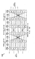
- FIG. 32 The transformations between various stages of the two network types are illustrated schematically in FIG. 32.
- the particular transformations identified in FIG. 32 are listed herein in Tables 1-3.
- the switch and output of stage i of a crossover network identified in block 1150 and the switch and output of a shuffle network stage i identified in block 1154 are related by transformations 1, 2, 3, and 4 of block 1152.
- the switch and input for stage i + 1 of a crossover network represented in block 1160 and the switch and input for stage i + 1 of a shuffle network represented in block 1164 are related as defined by transformations 9, 10, 11, and 12 of block 1162.
- stage i switch and output number for a crossover network and stage i + 1 switch and input number for a crossover network are specified by transformations 13, 14, 15, and 16 of block 1156.
- the corresponding relationships between successive stages of a shuffle network are given by transformations 5, 6, 7, and 8 of block 1158.
- the transformations 1 through 16 are listed in Tables 1-3.
- the number to be transformed is an n-bit binary number represented by B n-1 ⁇ B,Bo.
- FIG. 38 Arrangements for controlling a 512x512 crossover network 1200 (FIG. 38) are now described. To get a better understanding of the size of such a network, first refer to the 16x16 crossover network 1170 (FIGS. 34-36) and note the pattern of crossover connections from stage to stage.
- FIG. 37 is a representation of the relative sizes of the 16x16 network 1170 and the 512x512 network 1200. Also shown is an intermediate size 128x128 network.
- a crossover network controller 1300 is used to effect path hunt, connect, and disconnect functions for network 1200 via a plurality of stage controllers 1201 through 1209, individual to the stages 4 through 12.
- the nodes of the switching stages 4 through 12 are full capacity switching nodes such as the node of FIG. 5.
- the nodes of the fanout stages 1, 2 and 3 and the nodes of the fanin stages 13, 14, and 15 are simple fanout elements and fanin elements, respectively.
- Crossover network controller 1300 which may be implemented as a single processor operated under stored program control or as a hardware logic circuit arrangement, implements the control processing shown, for example, in FIGS. 39 and 40 to effect connections and disconnections respectively.
- Connection processing begins when a network 1200 inlet/outlet pair for a given connection request is stored in a queue in block 1402.
- a conversion of the inlet and outlet numbers is made in block 1404 to the corresponding inlet and outlet numbers of the shuffle network topologically equivalent to network 1200.
- a disjoint path check is made using procedures described further herein to determine whether any of the possible paths for this connection request intersect with any of the possible paths for other connection requests being processed concurrently. If there is no conflict with other connection requests in progress, execution proceeds to block 1408 where the switches or links associated with all paths from the inlet to the outlet of the equivalent shuffle network are determined.
- the switches are full capacity switches, it is sufficient to determine the links of a given path through the network. If the network switches are capacity one switches, it is sufficient to determine the switches of a given path through the network.
- an idle path is identified in block 1410 if such idle path exists.
- a path memory is updated in block 1412 to define the idle path using the inlet, outlet, and path numbers for the equivalent shuffle network. Connection orders are sent in block 1414 to the network stage controllers 1201 through 1209. Further, the path components (switches or links) for the identified path are marked busy in block 1416 for all stages.
- Disconnection processing begins when a network 1200 inlet for a given disconnection request is stored in a queue in block 1440.
- a conversion of the inlet number is made in block 1442 to the corresponding inlet number of the shuffle network topologically equivalent to network 1200.
- the shuffle inlet number is used to index the path memory to determine the shuffle outlet number and the path number for the connection.
- Disconnect orders are sent in block 1448 to the network stage controllers 1201 through 1209. Further, the path components (switches or links) for the path being disconnected are again marked idle for all stages.
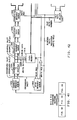
- FIGS. 42-44 A hardware embodiment of network controller 1300 is shown in FIGS. 42-44.
- Connection requests specifying a particular network 1200 inleboutlet pair, are stored in a connect request queue 1302.
- the nine-bit binary crossover inlet number and the nine-bit binary crossover outlet number are transmitted to a crossover to shuffle mapping unit 1304 (FIG. 50) for conversion to the corresponding nine-bit shuffle inlet number and the corresponding nine-bit shuffle outlet number.
- the shuffle inlet and outlet numbers are stored in a connect/disconnect request queue 1305 and then transmitted to a disjoint path check unit 1306 (FIG. 46).
- Unit 1306 determines whether the present inlet/outlet number pair defines paths through network 1200 which are link disjoint from the paths associated with another inleboutlet number pair. When two or more connection requests define disjoint paths through network 1200, multiple connection requests and path hunts can be processed at the same time in what is referred to herein as an overlap mode of operation. The shuffle inlet-outlet numbers are then stored in a connect/disconnect request queue 1308. When a path hunt is to be performed, connect request queue 1308 transmits a read request signal to a plurality of memories 1312 that store the link busy/idle bits for a corresponding one of the link stages 4 through 11 of network 1200.
- Link stage i is the stage of links between node stage i and node stage i + 1.
- the nine-bit shuffle inlet and the nine-bit shuffle outlet signals are also transmitted in parallel from connect request queue 1308 and predetermined ones of the inlet and outlet signals are used to address locations of the memories 1312.
- the blocked path indicator is fed back to the connect request queue 1302 such that the connection request can be repeated at a later time.
- the inverse of the blocked path indicator is used as a write request signal to write a busy bit into each of the memories 1312.
- the idle path number is transmitted to the memories 1312 to additionally identify the particular path and therefore the particular bit of the location addressed by the inlet and outlet numbers.
- a path memory 1318 is updated in response to the write request and stores, at an address defined by the shuffle inlet, both the shuffle outlet and the selected idle path number.
- N-input, N-output networks including a fanout section (expansion), a switching section and a fanin section (concentration) (FIG. 2) are considered. Every node stage in the switching section has NF/2 two-input, two-output switching nodes.
- the fanout section multiples each of the N inputs to F links at the input of the switching section. Accordingly there are FN links entering the switching section.
- the switching section contains S node stages with each node stage interconnected to the preceding node stage and the succeeding node stage with perfect shuffle equivalent interconnections.
- the fanin section groups together sets of F links and connects each group of F links to a different one of the N outputs.
- Network 2101 (FIG. 52) uses crossover interconnections and network 2102 (FIG. 53) uses shuffle interconnections. Note that the nodes in the two-dimensional crossover network 2101 are renumbered such that network 2101 has the same node connectivity as the two-dimensional shuffle network 2102. Also note that the shuffle interconnections are invariant from link-stage to link-stage, while the crossover interconnections vary from link-stage to link-stage.
- a three-dimensional crossover network 2110 (FIGS. 55-57) is topologically equivalent to the two-dimensional crossover network 1170 of FIGS. 34-36.
- network 1170 note that each node of a given node stage is labeled with a number from 0 through 31. Since network 1170 is a half-crossover network, it includes both crossover connections and straight connections. If the node numbers 0 through 31 are represented as the binary addresses 00000 through 11111, the crossover connections are such that a node in one stage is connected to the node in the next stage having a binary address differing in each of the p low order bit positions, where p is a positive integer at most equal to five.
- node 0 (00000) in stage 0 is connected to node 1 (00001) in stage 1
- node 0 (00000) in stage 1 is connected to node 3 (00011) in stage 2
- node 0 (00000) in stage 2 is connected to node 7 (00111) in stage 3
- node 0 (00000) in stage 3 is connected to node 15 (01111) in stage 4
- node 0 (00000) in stage 4 is connected to node 31 (11111) in stage 5
- node 0 (00000) in stage 5 is connected to node 1 (00001) in stage 6
- node 0 (00000) in stage 6 is connected to node 3 (00011) in stage 7
- node 0 (00000) in stage 7 is connected to node 7 (00111) in stage 8.
- each node in one stage is connected to the node in the next stage having the same binary address.
- the three-dimensional crossover network 2110 achieves the same node connectivity as two-dimensional crossover network 1170 (FIGS. 34-36) when the node numbers 0 through 31 are associated with successive nodes of rows and in opposite direction across successive rows in serpentine fashion.
- certain stages are interconnected with only horizontal connections (only nodes in the same row are interconnected) and the other stages are interconnected with only vertical connections (only nodes in the same column are interconnected).
- the crossover connections are defined as follows: when the binary addresses corresponding to the integers from zero through RC-1 are respectively associated with successive nodes of rows and in opposite directions across successive rows in serpentine fashion, each node in one array is connected to the node in the successive array having a binary address differing in each of the p low order bit positions, p being a positive integer at most equal to log 2 (RC).
- Photonic system 10 is implemented using 2-modules as the switching nodes (unlike network 1170 of FIGS. 34-36 which was assumed to have full capacity nodes). System 10 is controlled such that any given 2-module has only one active input at any time.
- 2-modules are described herein along with optical counterparts.
- NOR/OR implementation 2132 (FIG. 67) combines the two data inputs at a NOR gate, complementing the sense of the incoming data as it is transmitted through the NOR gate. The complemented data is transmitted to an OR gate, where it is combined with the disable control signal. When the disable control signal is low (0), the complemented data is transmitted to the two outputs. When the disable control signal is high (1), the 2-module is disabled and the outputs are held at logic one. One of the two NOR gate inputs must be a disabled logic zero signal from the 2-module in the previous stage. Since the NOR/OR 2-module implementation generates a logic one at its disabled output, a second type of 2-module is required that generates a logic zero at its disabled output.
- the new state of the S-SEED is read out and transmitted to the next stage.
- the clock signal is modulated and reflected from the windows with two unequal intensities that represent the dual-rail information presently stored in the S-SEED.
- the Q output power exceeds the Q output power when the S-SEED is set; the Q output power exceeds the Q output power when the S-SEED is reset.
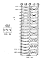
- An S-SEED array 500 shown in FIG. 58 is used to implement each of the node stages of network 2110 (FIGS.
- the preset, write, and read period durations are determined by the pulse rate of the laser diodes that generate the clock or power signal, the preset signal, and the disable signal (a continuous disable signal may also be used). Timing control of the electronic clock signals which drive laser diodes 301,401 and 451 is provided by the circuit of FIG. 73.
- the output pulse of a one-shot 452 of FIG. 73 has a duration T shot , which is typically less than one-fourth of a bit period, and is synchronized to the data bit stream.
- the circuit of FIG. 74 may be used to drive the lasers in, for example, three stages of the system if appropriate delay lines (not shown) are added to the electronic signal paths to account for the optical propagation delays between stages.
- the M-SEED approach has an advantage in that it only requires two lasers (one for the clock or power signals and one for the enable signals) whereas the S-SEED approach uses three lasers (one for the clock or power signals, one for the disable signals and one for the preset signals).
- the M-SEED approach requires three diodes rather than two; accordingly, the system optics must image larger fields when the M-SEED approach is followed.
- the S-SEED approach is used in photonic system 10 of FIG. 1.
- the relationship between the orientation of the S-SEED and the orientation of the plane containing the crossing links in a crossover connection has an impact on the design of the overall network. This relationship determines the types of 2-modules (NOR/OR or NAND/AND) that are used in particular stages of the network. Assume that the S-SEEDs are oriented vertically as shown in FIG. 58.
- the horizontal crossover connection is then defined to be a crossover connection where the crossing links form a plane that is perpendicular to the line formed by the S-SEED diodes.
- the vertical crossover connection is defined to be a crossover connection where the crossing links form a plane that is parallel to the line formed by the S-SEED diodes.
- a modification of optical hardware module 51 of FIG. 93 is used to provide the vertical crossover stages.
- the prismatic mirror that provides the crossing connections is rotated by 90 degrees about the optical axis.
- the prismatic mirror array is rotated by 90 degrees.
- the V-grooves of the prismatic mirror array are oriented horizontally to provide vertical shifts.
- the crossing connections within the vertical crossover stages also cross the data rails. Crossing the rails within a dual-rail system is equivalent to complementing the data bits. If the straight connections were implemented with a mirror as in FIG. 93, the data bits traveling along the straight connections would not be complemented.
- the data bits within the straight connections of the vertical crossover stages are also complemented by crossing the dual rails. This is accomplished by replacing mirror 108 of FIG. 93 by a prismatic mirror array with very narrow V-grooves. The width of these grooves matches the spacing between the S-diode and the R-diode and thus reverses the positions of the outputs of each S-SEED thereby inverting the dual-rail data.
- the resulting vertical crossover connections between two consecutive S-SEED arrays are shown in FIG. 77.
- the 2-modules on either side of a horizontal crossover stage are designed differently than the 2- modules on either side of a vertical crossover stage.
- the sense of the disabled output data is controlled to ensure that the disabled data entering a NOR/OR 2-module is a logic one, while the disabled data entering a NAND/AND 2-module is a logic zero.
- NOR/OR 2-module is a logic one
- NAND/AND 2-module is a logic zero.
- the disabled output (logic one) of a NOR / OR 2-module is complemented by the vertical crossover and passed as a logic one directly into the input of a NOR/OR 2- module in the next stage.
- the disabled output (logic zero) of a NAND/AND 2-module is complemented by the vertical crossover and passed as a logic zero directly into the input of a NAND/AND 2-module in the next stage.
- the 2-modules on either side of a vertical crossover stage should both be of the same type (NOR/OR or NAND / AND).
- the data streams passed through the network are complemented many times as they are routed through the multi-stage network. Complementing occurs at every node stage due to the function of the NOR and NAND gates and complementing also occurs in vertical crossover link stages. All of the complementing operations must be accounted for in the overall network. If the data is complemented an odd number of times as it passes through the network, one more complementing function is added to correct the sense of the data. This additional complementing function may be provided, for example, by adding an extra stage of 2-modules, by adding an extra stage of connections that cross rails, by inverting the data in interface electronics at the network output or by alignment of the output fiber matrix with the appropriate S-SEED diode.
- FIG. 78 shows a single path through the network.
- FIG. 79 shows a line of linked 2-modules comprising the 2-modules of the single path of FIG. 78 and the associated disabled 2-modules.
- the sense of the data at various points through the network is shown.
- the complementing in the vertical link stages is also shown.
- the data is complemented. Accordingly, the data must be complemented one additional time at the output of the network to return to its initial form.
- the other 2-module in stage j + 1 is disabled. Assume that 2- module C is enabled and 2-module D is disabled. The other 2-module (B) in node stage j that is connected to 2-module D cannot pass data through 2-module D, even though 2-module D is not carrying an active data path. If 2-module D is enabled to carry data from 2-module B, the data arriving at the input of 2- module D from 2-module B is corrupted by the data also arriving at 2-module D from 2-module A. Thus 2- module D is corrupted by the active data path that routes data from 2-module A to 2-module C. Accordingly, 2-module B may not be used.
- Each S-SEED array 500 within photonic system 10 requires the following: 1) relaying the data input images onto the S-SEEDs, 2) relaying the power input images onto the S-SEEDs, 3) relaying the control input images onto the S-SEEDs, 4) data connections (crossover alignment network), 5) beam combination for data, power and control inputs, and 6) data outputs to the next stage.
- These requirements are substantially the same for each S-SEED array; accordingly the optical hardware modules used to meet the requirements for each stage have few variations.
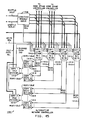
- FIG. 81 is a functional block diagram of a portion of photonic system 10.
- the data signals on the input fibers are conditioned and spatially aligned by the data input unit 40.
- the crossover interconnections required for the various stages are provided by the optical crossover interconnection unit 100.
- Arrays of spots which form the power and control inputs are generated by the power and control units 300 and 400. All of the spot arrays (data or information signal, power or clock, and control) are combined into a single spot array to be imaged onto the S-SEED arrays 500. This combination is performed by the beam combination unit 200.
- the S-SEED array 500 selectively reflects the power signals and beam combination unit 200 redirects the reflected power signals as input data signals to the next stage.
- the S-SEED arrays are interconnected in perfect shuffle equivalent fashion using optical crossover interconnect unit 100 shown in FIG. 82.
- network 1170 FIGS. 34-36
- the size of the cross varies from stage to stage, and in the three-dimensional crossover network 2110 (FIGS. 55-57), the direction of the cross also varies.
- FIG. 82 shows the optical arrangement used to implement optical crossover interconnect 100.
- the input image (shown entering from the bottom in FIG. 82) is circularly polarized when it passes through lens 101 to polarization beam splitter (PBS) 102, where it is split into two copies.
- PBS polarization beam splitter
- the copy passing through PBS 102 is linearly polarized (p-type) (parallel polarization) until it passes through quarter-wave plate (QWP) 106 and becomes circularly polarized.
- Lens 107 focuses it to a spot array on plane mirror 108. Reflecting off mirror 108, the image returns through QWP 106.
- the image is linearly polarized (s-type) (perpendicular polarization) and is reflected by PBS 102.
- the other image copy initially reflected by PBS 102, follows a similar path through QWP 103 and lens 104, except that it is imaged onto a prismatic mirror (PM) 105.
- PM 105 reverses the image about the axis of its corner, as well as reflecting the image back toward lens 104.
- This reversed and reflected image is collected by lens 104 and passes again through QWP 103.
- the polarization of the reflected image is rotated and the image passes through PBS 102 on its return trip. At the output, the two image copies are recombined into a single, overlapped image.
- connection of FIG. 83 is formed, where the reversed image forms the crossed connections, and the other image, the straight connections.
- the width of the cross is varied from stage to stage.
- One means of realizing this is by replacing the prismatic mirror 105 with a prismatic mirror array (PMA) 110 as in FIG. 84.
- PMA prismatic mirror array
- each prism facet reverses or crosses a portion of the image.
- the width of the facets is varied.
- Some system stages effect horizontal crossovers and the other stages effect vertical crossovers.
- the vertical crossovers are achieved by rotating the PMAs by 90 degrees so that the spot array images are reversed about horizontal, rather than vertical axes.
- the crossover connections which are parallel to the line joining the S and R diodes of the S-SEEDs are referred to as vertical crossovers and the connections perpendicular to this line are referred to as horizontal crossovers.
- the vertical crossovers not only interconnect the S-SEEDs but also invert the positions of the S and R diodes forming the S-SEEDs. This causes a data inversion within the vertical cross connections and thus requires that a similar data inversion be implemented for the companion straight connections. This is accomplished by replacing plane mirror 108 with a PMA with very narrow V-grooves. The width of these grooves matches the S-R diode spacing and thus reverses the positions of the S and R outputs of each S-SEED, thereby inverting the dual rail data. In all cases, the overall size, shape, and input/output interfaces of the optical crossover interconnect unit 100 remains the same, which significantly eases system integration.
- optical hardware module 51 which implements a horizontal crossover having a single cross.
- prismatic mirror 105 is replaced by a prismatic mirror array having two V-grooves to implement a horizontal crossover having two crosses.
- plane mirror 108 is replaced with a prismatic mirror array having narrow V-grooves to perform the data inversion necessary for vertical crossover stages.
- the prismatic mirrors or prismatic mirror arrays are rotated by 90 degrees as required to effect vertical crossovers.
- the data signals passed from one stage to the next take the form of two-dimensional arrays of spots.
- the power inputs, which effect the signal amplification, and the control inputs, which determine the mode of device operation and control the establishment of network paths, also have the form of two-dimensional spot arrays.
- the optical arrangement shown in FIG. 85 is used to generate an array of uniform intensity spots of good contrast.
- a single laser beam generated by laser diode 301 is collimated by lens 302 and is incident upon gratings 303, which split the beam into many uniform intensity beams. These beams are focused by lens 304 into an array of spots in the focal plane of lens 304.
- the uniform spots occupy a central region of the plane and are surrounded by non-uniform, lower intensity spots.
- the unwanted, non-uniform spots are blocked out by spatial filter 305.
- the spots in the central region pass through spatial filter 305 and are recollimated by lens 306 to form an array of beams.
- This array is incident on the multiple-imaging gratings 307 which split the array into many uniform copies. When these copies are ultimately focused into spots on S-SEED array 500, many abutted copies of the original central region spot array are produced.
- a large uniform spot array is achieved by abutting many uniform copies of a small uniform spot array.
- the control (preset and disable) spot arrays are formed having a lower wavelength (780 nanometers) than the nominal S-SEED operating wavelength (850 nanometers).
- the spots in the preset spot array are imaged onto only one diode of each S-SEED in the S-SEED arrays, rather than onto both diodes as the power spots are. Since fewer spots are formed per array, the spots may have more optical power than the spots of the power spot array if laser diodes having the same power output are used; alternatively, lower power laser diodes may be used for the preset beams.
- the optical arrangement used to generate the disable spot array is shown in FIG. 86.
- the portion of the arrangement comprising laser diode 401, lens 402, gratings 403, lens 404, spatial filter 405, lens 406, and gratings 407 is substantially identical to the arrangement of FIG. 85.
- Lens 408 is placed immediately after gratings 407 to focus the beam array to a spot array on spatial light modulator 409.
- the spots which are passed by spatial light modulator 409 are recollimated into a space-variant beam array by lens 410. These beams are ultimately refocused onto S-SEED array 500.
- the configuration of spatial light modulator 409 changes to disable or enable different 2-modules.
- PMR 213 is an array of small mirrors deposited on a transparent substrate. The size of the mirrors matches the spot size and the mirrors are positioned such that the reflected spots are imaged by the rest of the beam combination optics onto one diode of each S-SEED. After the spots reflect off PMR 213, they are recollimated by lens 212 and pass through QWP 211 a second time. This second pass again retards the perpendicular component by another one-quarter wavelength, thus converting the beams to p-type (parallel) linear polarization and the beams pass through PBS 216.
- the preset beam array generation is oriented such that the beams enter sub-unit 210 with p-type linear polarization.
- QWP 215 retards the polarization component perpendicular to its fast axis by one-quarter wavelength and converts the beams to circular polarization.
- Lens 214 focuses the beams to spots on transparent areas of PMR 213. These spots are positioned such that they are imaged onto the S-SEED diodes that do not have disable spots.
- the preset spots pass through PMR 213 and are recollimated by lens 212.
- QWP 211 is oriented with its fast axis at 90 degrees with respect to QWP 215.
- QWP 211 retards the other polarization component (the one not retarded by QWP 215) by one-quarter wavelength and returns the beam array to its original p-type linear polarization.
- the preset beams pass through PBS 216.
- the two beam arrays are combined into the same aperture and onto the same polarization. Since the spots are imaged through a glass plate, spherical aberration can accumulate. If the plate is thin (approximately 1 mm) and lenses with focal lengths more than 30 mm are used, the spherical aberration is not significant.
- the depth of focus of the spot array image at PMR 213 is relatively large (greater than 16 microns), thus easing the alignment tolerances for PMR 213.
- Beam combination sub-unit 240 (FIG. 88) combines the control beam array (preset and disable) with the power beam array.
- a dichroic or wavelength-selective mirror (DM) 243 is used rather than a spatially-selective (space-variant) mirror.
- DM 243 reflects 850-nanometer light and transmits 780-nanometer light. Similar to the disable beams in sub-unit 210 (FIG. 87), the power beams enter sub-unit 240 (FIG. 88) with linear polarization of s-type, reflect off PBS 241 (designed for 850-nanometer operation) and DM 243, then pass through PBS 241 and exit having p-type linear polarization.
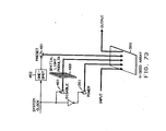
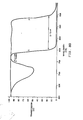
- FIG. 90 is a plot of typical transmission curves for a PBS designed for 850-nanometer operation.
- a variation in the angle of incidence corresponds to a variation in wavelength.
- the beam arrays used in the present embodiment may have a substantial angular field, for example, of plus or minus five degrees.
- the solution effected in the present embodiment is to transmit both the 780-nanometer beams and the 850-nanometer beams with p-type linear polarization.
- the optical apparatus of sub-unit 240 (FIG. 88) is used because DM 243 is relatively insensitive to polarization and angle of incidence when used at approximately zero degrees.
- the power/control beam array is passed onto the S-SEEDs in the same manner as the preset beams in FIG. 87.
- the power/control beams are focused through the transparent areas of PMR 274 adjacent to the mirrors as shown in FIG. 91. Thus, they are incident on the S-SEED input windows adjacent to the signal spots as in FIG. 92.
- the preset and disable spots are focused on different diodes of each S-SEED, and with the signal spots, set the state of the S-SEED.
- the power spots read out the dual-rail state of each S-SEED.
- the reflected output beams are then imaged through the transparent areas of PMR 278 adjacent to the mirrors.
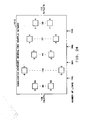
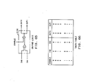
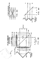
- FIG. 98 An alternative optical arrangement for performing wavelength-dependent beam combination is shown in FIG. 98 as comprising PBS 8101, QWP 8102, DM 8103, and QWP 8104.
- PBS 8101, QWP 8102 and QWP 8104 are designed for 850-nanometer operation.
- the combined power and control beams both have s-type linear polarization.
- FIG. 99 A second alternative optical arrangement for performing wavelength-dependent beam combination is shown in FIG. 99 as comprising PBS 8201, QWP 8202, DM 8203, and QWP 8204.
- PBS 8201, QWP 8202 and QWP 8204 are designed for 780-nanometer operation.
- the combined power and control beams both have s-type linear polarization.
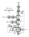
- FIG. 100 A further alternative optical arrangement for performing wavelength-dependent beam combination in shown in FIG. 100 as comprising PBS 8301, QWP 8302, DM 8303, QWP 8304, QWP 8305, DM 8306, and QWP 8307.
- PBS 8301, QWP 8302, QWP 8304, QWP 8305, and QWP 8307 are designed for 850- nanometer operation.
- Two of the combined beams have s-type linear polarization and the other two of the combined beams have p-type linear polarization.
Landscapes
- Physics & Mathematics (AREA)
- General Physics & Mathematics (AREA)
- Optics & Photonics (AREA)
- Optical Communication System (AREA)
- Data Exchanges In Wide-Area Networks (AREA)
- Use Of Switch Circuits For Exchanges And Methods Of Control Of Multiplex Exchanges (AREA)
- Optical Head (AREA)
Applications Claiming Priority (2)
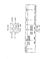
| Application Number | Priority Date | Filing Date | Title |
|---|---|---|---|
| US349275 | 1982-02-16 | ||
| US07/349,275 US5036512A (en) | 1989-05-08 | 1989-05-08 | Optical apparatus for combining light beam arrays having different wavelengths |
Publications (3)
| Publication Number | Publication Date |
|---|---|
| EP0397369A2 true EP0397369A2 (fr) | 1990-11-14 |
| EP0397369A3 EP0397369A3 (fr) | 1992-03-25 |
| EP0397369B1 EP0397369B1 (fr) | 1995-12-20 |
Family
ID=23371645
Family Applications (1)
| Application Number | Title | Priority Date | Filing Date |
|---|---|---|---|
| EP90304726A Expired - Lifetime EP0397369B1 (fr) | 1989-05-08 | 1990-05-01 | Dispositif optique pour combiner des réseaux lumineux de longueurs d'ondes différentes |
Country Status (4)
| Country | Link |
|---|---|
| US (1) | US5036512A (fr) |
| EP (1) | EP0397369B1 (fr) |
| JP (1) | JPH07122699B2 (fr) |
| DE (1) | DE69024256T2 (fr) |
Cited By (1)
| Publication number | Priority date | Publication date | Assignee | Title |
|---|---|---|---|---|
| EP0436924A3 (en) * | 1989-12-27 | 1992-04-22 | Honeywell Inc. | Beam combining/splitter cube prism for color polarization |
Families Citing this family (13)
| Publication number | Priority date | Publication date | Assignee | Title |
|---|---|---|---|---|
| GB9012667D0 (en) * | 1990-06-07 | 1990-08-01 | Emi Plc Thorn | Apparatus for displaying an image |
| US5430561A (en) * | 1991-07-17 | 1995-07-04 | Fujitsu Limited | Optical space switch employing 2 parallel diffraction gratings and a polarization rotating element |
| US5528406A (en) * | 1991-08-02 | 1996-06-18 | Gpt Limited | Telecommunications switching device |
| US5886818A (en) * | 1992-12-03 | 1999-03-23 | Dimensional Media Associates | Multi-image compositing |
| US5552934A (en) * | 1994-03-18 | 1996-09-03 | Spm Corporation | Background reflection-reducing plano-beam splitter for use in real image projecting system |
| US6318868B1 (en) | 1997-05-01 | 2001-11-20 | Larussa Joseph A. | Interactive virtual image store window |
| US6421163B1 (en) * | 1998-11-05 | 2002-07-16 | Comptic, Inc. | Two dimensional transform generator |
| US6259560B1 (en) | 1999-04-16 | 2001-07-10 | The United States Of America As Represented By The Secretary Of The Navy | Continuously variable beam combiner |
| DE10122010B4 (de) * | 2000-05-08 | 2004-02-26 | Fraunhofer-Gesellschaft zur Förderung der angewandten Forschung e.V. | Anordnung zum Multiplexing und/oder Demultiplexing |
| US20020080741A1 (en) * | 2000-10-13 | 2002-06-27 | Akihiko Toyoshima | Multiple wireless format phone system and method |
| KR20100099747A (ko) * | 2007-12-28 | 2010-09-13 | 쓰리엠 이노베이티브 프로퍼티즈 컴파니 | 광 조합기 |
| WO2012057749A1 (fr) * | 2010-10-27 | 2012-05-03 | Hewlett-Packard Development Company, L.P. | Récepteurs et appareils émetteurs/récepteurs pour des systèmes à bus optiques multiples |
| US10690931B2 (en) * | 2018-05-25 | 2020-06-23 | Panasonic Intellectual Property Management Co., Ltd. | Light source device and projection display apparatus |
Family Cites Families (8)
| Publication number | Priority date | Publication date | Assignee | Title |
|---|---|---|---|---|
| JPS6221128A (ja) * | 1985-07-19 | 1987-01-29 | Matsushita Electric Ind Co Ltd | 光ヘテロダイン検波装置 |
| FR2598574B1 (fr) * | 1986-05-06 | 1992-02-28 | Matra | Procede et dispositif optiques de transmission de donnees a multiplexage de frequence |
| JPS63249818A (ja) * | 1987-04-06 | 1988-10-17 | Nippon Telegr & Teleph Corp <Ntt> | 光合分波器 |
| US4754132A (en) * | 1987-04-24 | 1988-06-28 | American Telephone And Telegraph Company, At&T Bell Laboratories | Symmetric optical device with quantum well absorption |
| JPS6423221A (en) * | 1987-07-20 | 1989-01-25 | Fujitsu Ltd | Multiplexing/demultiplexing unit and multiplexer/ demultiplexer for coherent light communication |
| JPS6429227A (en) * | 1987-07-27 | 1989-01-31 | Hitachi Heating Appl | High frequency heating apparatus |
| JP2573317B2 (ja) * | 1988-06-29 | 1997-01-22 | 日東電工株式会社 | 親水化多孔質膜 |
| US4917456A (en) * | 1988-07-15 | 1990-04-17 | At&T Bell Laboratories | Optical crossover network |
-
1989
- 1989-05-08 US US07/349,275 patent/US5036512A/en not_active Expired - Lifetime
-
1990
- 1990-05-01 EP EP90304726A patent/EP0397369B1/fr not_active Expired - Lifetime
- 1990-05-01 DE DE69024256T patent/DE69024256T2/de not_active Expired - Fee Related
- 1990-05-08 JP JP2116983A patent/JPH07122699B2/ja not_active Expired - Fee Related
Cited By (1)
| Publication number | Priority date | Publication date | Assignee | Title |
|---|---|---|---|---|
| EP0436924A3 (en) * | 1989-12-27 | 1992-04-22 | Honeywell Inc. | Beam combining/splitter cube prism for color polarization |
Also Published As
| Publication number | Publication date |
|---|---|
| EP0397369B1 (fr) | 1995-12-20 |
| DE69024256D1 (de) | 1996-02-01 |
| US5036512A (en) | 1991-07-30 |
| JPH07122699B2 (ja) | 1995-12-25 |
| JPH0339927A (ja) | 1991-02-20 |
| EP0397369A3 (fr) | 1992-03-25 |
| DE69024256T2 (de) | 1996-08-08 |
Similar Documents
| Publication | Publication Date | Title |
|---|---|---|
| EP0397372B1 (fr) | Topologie de réseau pour blocage réduit et un système photonique mettant en oeuvre celle-ci | |
| US5258978A (en) | Space-division switching network having reduced functionality nodes | |
| US5023864A (en) | Crossover network utilizing two-dimensional arrays of nodes | |
| EP0397368B1 (fr) | Procédé de commande d'un réseau de commutation à division spatiale | |
| EP0397369B1 (fr) | Dispositif optique pour combiner des réseaux lumineux de longueurs d'ondes différentes | |
| EP0590877B1 (fr) | Réseau de distribution de paquets optique à plusieurs étages avec commutateur de dérivation | |
| JP2918772B2 (ja) | パケット交換配置 | |
| JPH06214278A (ja) | 光インターコネクションネットワーク | |
| EP0229177B1 (fr) | Agencement de permutation optique | |
| EP0501647B1 (fr) | Dispositif de commande de réseau | |
| US4917456A (en) | Optical crossover network | |
| US6839472B1 (en) | Solid state optical interconnect system | |
| US5467211A (en) | Optoelectric sliding banyan network | |
| EP0501646B1 (fr) | Réseau à commande intégrée | |
| RU2088960C1 (ru) | Многокаскадный оптоэлектронный коммутатор | |
| Cloonan et al. | A 3D crossover switching network based on S-SEED arrays | |
| KR0149858B1 (ko) | 노드 및 링크의 다수 스테이지와 확장 및 집속 수단을 포함하고 있으며 최소 2개의 경로를 가지고 있는 시스템 | |
| CN101216603A (zh) | 一种集成多级二维光学微机电系统光开关 |
Legal Events
| Date | Code | Title | Description |
|---|---|---|---|
| PUAI | Public reference made under article 153(3) epc to a published international application that has entered the european phase |
Free format text: ORIGINAL CODE: 0009012 |
|
| AK | Designated contracting states |
Kind code of ref document: A2 Designated state(s): BE DE FR GB IT |
|
| PUAL | Search report despatched |
Free format text: ORIGINAL CODE: 0009013 |
|
| AK | Designated contracting states |
Kind code of ref document: A3 Designated state(s): BE DE FR GB IT |
|
| 17P | Request for examination filed |
Effective date: 19920911 |
|
| 17Q | First examination report despatched |
Effective date: 19940208 |
|
| RAP3 | Party data changed (applicant data changed or rights of an application transferred) |
Owner name: AT&T CORP. |
|
| GRAA | (expected) grant |
Free format text: ORIGINAL CODE: 0009210 |
|
| AK | Designated contracting states |
Kind code of ref document: B1 Designated state(s): BE DE FR GB IT |
|
| PG25 | Lapsed in a contracting state [announced via postgrant information from national office to epo] |
Ref country code: BE Effective date: 19951220 Ref country code: IT Free format text: LAPSE BECAUSE OF FAILURE TO SUBMIT A TRANSLATION OF THE DESCRIPTION OR TO PAY THE FEE WITHIN THE PRE;WARNING: LAPSES OF ITALIAN PATENTS WITH EFFECTIVE DATE BEFORE 2007 MAY HAVE OCCURRED AT ANY TIME BEFORE 2007. THE CORRECT EFFECTIVE DATE MAY BE DIFFERENT FROM THE ONE RECORDED.SCRIBED TIME-LIMIT Effective date: 19951220 Ref country code: FR Effective date: 19951220 |
|
| REF | Corresponds to: |
Ref document number: 69024256 Country of ref document: DE Date of ref document: 19960201 |
|
| EN | Fr: translation not filed | ||
| PLBE | No opposition filed within time limit |
Free format text: ORIGINAL CODE: 0009261 |
|
| STAA | Information on the status of an ep patent application or granted ep patent |
Free format text: STATUS: NO OPPOSITION FILED WITHIN TIME LIMIT |
|
| 26N | No opposition filed | ||
| PGFP | Annual fee paid to national office [announced via postgrant information from national office to epo] |
Ref country code: GB Payment date: 20010426 Year of fee payment: 12 |
|
| PGFP | Annual fee paid to national office [announced via postgrant information from national office to epo] |
Ref country code: DE Payment date: 20010629 Year of fee payment: 12 |
|
| REG | Reference to a national code |
Ref country code: GB Ref legal event code: IF02 |
|
| PG25 | Lapsed in a contracting state [announced via postgrant information from national office to epo] |
Ref country code: GB Free format text: LAPSE BECAUSE OF NON-PAYMENT OF DUE FEES Effective date: 20020501 |
|
| PG25 | Lapsed in a contracting state [announced via postgrant information from national office to epo] |
Ref country code: DE Free format text: LAPSE BECAUSE OF NON-PAYMENT OF DUE FEES Effective date: 20021203 |
|
| GBPC | Gb: european patent ceased through non-payment of renewal fee |
Effective date: 20020501 |