EP0397937A2 - Système et procédé de commande pour équipement de test paramétrique automatisé - Google Patents
Système et procédé de commande pour équipement de test paramétrique automatisé Download PDFInfo
- Publication number
- EP0397937A2 EP0397937A2 EP89304955A EP89304955A EP0397937A2 EP 0397937 A2 EP0397937 A2 EP 0397937A2 EP 89304955 A EP89304955 A EP 89304955A EP 89304955 A EP89304955 A EP 89304955A EP 0397937 A2 EP0397937 A2 EP 0397937A2
- Authority
- EP
- European Patent Office
- Prior art keywords
- test
- wafer
- devices
- measurement
- control system
- Prior art date
- Legal status (The legal status is an assumption and is not a legal conclusion. Google has not performed a legal analysis and makes no representation as to the accuracy of the status listed.)
- Withdrawn
Links
Images




Classifications
-
- G—PHYSICS
- G01—MEASURING; TESTING
- G01R—MEASURING ELECTRIC VARIABLES; MEASURING MAGNETIC VARIABLES
- G01R31/00—Arrangements for testing electric properties; Arrangements for locating electric faults; Arrangements for electrical testing characterised by what is being tested not provided for elsewhere
- G01R31/28—Testing of electronic circuits, e.g. by signal tracer
- G01R31/317—Testing of digital circuits
- G01R31/3181—Functional testing
- G01R31/3183—Generation of test inputs, e.g. test vectors, patterns or sequences
- G01R31/318307—Generation of test inputs, e.g. test vectors, patterns or sequences computer-aided, e.g. automatic test program generator [ATPG], program translations, test program debugging
-
- G—PHYSICS
- G01—MEASURING; TESTING
- G01R—MEASURING ELECTRIC VARIABLES; MEASURING MAGNETIC VARIABLES
- G01R31/00—Arrangements for testing electric properties; Arrangements for locating electric faults; Arrangements for electrical testing characterised by what is being tested not provided for elsewhere
- G01R31/28—Testing of electronic circuits, e.g. by signal tracer
- G01R31/282—Testing of electronic circuits specially adapted for particular applications not provided for elsewhere
- G01R31/2831—Testing of materials or semi-finished products, e.g. semiconductor wafers or substrates
-
- G—PHYSICS
- G01—MEASURING; TESTING
- G01R—MEASURING ELECTRIC VARIABLES; MEASURING MAGNETIC VARIABLES
- G01R31/00—Arrangements for testing electric properties; Arrangements for locating electric faults; Arrangements for electrical testing characterised by what is being tested not provided for elsewhere
- G01R31/28—Testing of electronic circuits, e.g. by signal tracer
- G01R31/317—Testing of digital circuits
- G01R31/3181—Functional testing
- G01R31/319—Tester hardware, i.e. output processing circuits
- G01R31/31903—Tester hardware, i.e. output processing circuits tester configuration
- G01R31/31908—Tester set-up, e.g. configuring the tester to the device under test [DUT], down loading test patterns
-
- G—PHYSICS
- G01—MEASURING; TESTING
- G01R—MEASURING ELECTRIC VARIABLES; MEASURING MAGNETIC VARIABLES
- G01R31/00—Arrangements for testing electric properties; Arrangements for locating electric faults; Arrangements for electrical testing characterised by what is being tested not provided for elsewhere
- G01R31/28—Testing of electronic circuits, e.g. by signal tracer
- G01R31/317—Testing of digital circuits
- G01R31/3181—Functional testing
- G01R31/319—Tester hardware, i.e. output processing circuits
- G01R31/31903—Tester hardware, i.e. output processing circuits tester configuration
- G01R31/31912—Tester/user interface
-
- H—ELECTRICITY
- H10—SEMICONDUCTOR DEVICES; ELECTRIC SOLID-STATE DEVICES NOT OTHERWISE PROVIDED FOR
- H10P—GENERIC PROCESSES OR APPARATUS FOR THE MANUFACTURE OR TREATMENT OF DEVICES COVERED BY CLASS H10
- H10P74/00—Testing or measuring during manufacture or treatment of wafers, substrates or devices
- H10P74/23—Testing or measuring during manufacture or treatment of wafers, substrates or devices characterised by multiple measurements, corrections, marking or sorting processes
-
- G—PHYSICS
- G01—MEASURING; TESTING
- G01R—MEASURING ELECTRIC VARIABLES; MEASURING MAGNETIC VARIABLES
- G01R31/00—Arrangements for testing electric properties; Arrangements for locating electric faults; Arrangements for electrical testing characterised by what is being tested not provided for elsewhere
- G01R31/28—Testing of electronic circuits, e.g. by signal tracer
- G01R31/30—Marginal testing, e.g. by varying supply voltage
-
- G—PHYSICS
- G06—COMPUTING OR CALCULATING; COUNTING
- G06F—ELECTRIC DIGITAL DATA PROCESSING
- G06F2201/00—Indexing scheme relating to error detection, to error correction, and to monitoring
- G06F2201/865—Monitoring of software
Definitions
- the present invention relates to automatic test equipment, and more particularly to automated parametric test systems for determining the characteristics of integrated circuits during the development of processes for manufacturing such circuits. More specifically, the present invention is concerned with a system for controlling automated parametric testers in a manner which facilitates the development of tests and improves the documentation, reusability and maintainability of programs for performing testing routines.
- test shell in which different functional aspects of the parametric test operation are divided into separate components containing information that can be referred to, as needed, to carry out any desired test.
- the first component is data; the second two components are programs and subroutines.
- One subcomponent, the reference information contains fixed information relating to the configuration of a wafer to be tested, as well as specifications relating to the test equipment. Since this information does not change over time, it only needs to be entered into the system once and can be subsequently referred to as necessary to carry out test procedures.
- the measurement algorithm library contains the subroutines which perform each of the possible types of measurements that can be carried out on each available type of device. Again, these subroutines remain fixed from one wafer to another, and thus need only be programmed into the system once.
- test definition information can be directly provided to the system by the process engineer, and is conveniently entered by means of a suitable worksheet, either on paper or by means of a video display.
- the parametric test system includes a set of automated measurement instruments 10 which generate the appropriate voltage and current signals to be applied to devices on a wafer and measure the signals generated by the devices in response.
- the input and output terminals of the measurement instruments are connected to a relay matrix 12.
- the matrix selectively applies the output signals from the measurement instruments 10 to appropriate probe pins in a wafer prober 13. These pins are located on a probe card 14 and engage contact pads on the wafer 15 being tested.
- the wafer is positioned relative to the pins by means of a suitable X-Y positioning mechanism 17.
- the responding signals generated by the devices on the tested wafer appear at the same or other pins on the wafer prober, and are similarly applied to the measurement instruments 10 by means of the relay matrix 12.
- the controller 16 controls the positioning of the pins in the wafer prober to place them at a desired location on the tested wafer.
- the controller 16 can be a suitable desktop computer, for example, which executes a test program stored in its memory such as that provided by the present invention.
- An input/output device 18 can be used to enter reference and test definition information into files, serve as the operator interface during test execution and display reports relating to the response of the tested wafer.
- a control program stored in the memory of the controller 16 for controlling a system of the type illustrated in Figure 1 in accordance with the principles of the present invention is comprised of three major components which can be divided into two functional subsystems.
- One subsystem involves the definition of tests, and is comprised of a configuration file library 20 and a measurement algorithm library 22.
- the other subsystem relates to test execution, and is comprised of a general test program 24.
- the configuration file library 20 contains two basic types of information, reference information and test definition information.
- the reference information involves a complete description of the devices on a wafer to be tested and the equipment which implements the tests. Since the structure of the wafer and the equipment remains fixed after it has been produced, this information need only be entered into the configuration file library once, and can be shared by all of the process engineers who desire to perform different tests on the wafer.
- Test definition information that is also stored in the configuration file library 20 describes the individual tests that are to be performed on specific devices on the wafer. These tests can be different for each engineer who accesses the system.
- the measurement algorithm library 22 consists of a set of subroutines.
- the main purpose of each of these subroutines is to perform specific device measurements, but they are not limited to that function.
- one subroutine may describe the sequence of steps necessary to measure the threshold voltage of an FET, and another subroutine may describe the test procedure for measuring diode leakage current.
- Other measurement algorithm subroutines can be written to print special reports, plot test data to the video screen or perform calculations on the data such as linear regressions.
- the general test program 24 interprets the information stored in the configuration file library 20 and calls subroutines from the measurement algorithm library 22 to perform actual wafer testing.
- This program contains standardized versions of all administrative functions common to each test, such as hardware initialization, operator interface, measurement sequencing, data routing and storage, etc.
- the general test program 24 positions the wafer prober 14 and accesses the appropriate measurement algorithms which switch the relay matrix 12 and control the actuation of the measurement instruments to carry out the desired testing.
- the general test program also generates appropriate output reports on the input/output device 18.
- each engineer need only be concerned with that aspect of the program which pertains to his particular area of expertise.
- the process engineer who is only interested in the results of certain tests does not have to be generally familiar with the overall layout of the wafer in order to obtain the information he desires. Rather, the layout information can be entered into the program by the mask engineer who is most familiar with it.
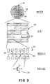
- the layout of a wafer is illustrated in a hierarchical form.
- Each wafer 26 consists of a two-dimensional array of dice 28. Generally, a wafer might contain 100-200 dice. Typically, every die on a wafer will be the same, although it is possible to have the dice vary from one another.
- Each die consists of an arrangement of modules 30, which can be the same or different from one another.
- a module is defined as the largest area that can be covered by the set of probe pins in the wafer prober.
- Each module consists of one or more devices 32, e.g. transistors, diodes, resistors, etc. having terminals connected to contact pads within the module.
- the mask engineer can fill out a series of worksheets (either on paper or directly into computer memory by means of a video display) that are respectively related to the tiers of the hierarchy shown in Figure 3.
- One worksheet referred to as a wafer layout worksheet, can describe information such as the wafer dimension, die-to-die distances, and die outlines.
- this worksheet identifies the specific location of each die relative to a reference position defined by the user. This reference position can be on the wafer itself, or at a location that is not on the wafer but is fixed relative thereto.
- the positions of the dice, and more particularly a specific point on each die such as a corner can be specified by means of a first set of X-Y coordinates whose origin is the reference position, to thereby accommodate non-uniform die spacing on the wafer.
- a second type of worksheet can define the arrangement of modules within each type of die.
- a module coordinate worksheet can be employed to describe the location of each module within the die.
- this worksheet can describe the number of contact pads, their dimensions, relative arrangement and the distances between contact pads.
- a precise location on one of the pads, such as its center, can also be identified for reference purposes.
- this location is identified using a second X-Y coordinate designator.
- the origin of this coordinate system could be the specific point on the die, e.g. a corner, that is identified by means of the first coordinate pair described previously.
- any point on the wafer can be specified by means of two vectors, the first of which points to a particular die and the second of which identifies the point within the die.
- a module design worksheet can be employed to describe the arrangement and construction of devices that are located within each type of module.
- Each device within the module can be labeled, and each of its terminals can be assigned to one of the pads in a previously defined pad pattern layout for the module.
- each pad in a given pad pattern can be correlated with one of the pins on the probe card as well as its associated contact point within the relay matrix.
- An advantage of the methodology of the worksheet layout is that it enables the engineers to enter information and construct tests in terms that are familiar to them.
- the engineers can write the reference and test definition information either on paper worksheets or directly onto the video display "worksheet".
- the information contained in them is stored in structured files within the configuration file library 20.
- the worksheets are organized in a manner which corresponds to the format of the files in the library. This approach reduces the level of skill required to store the information in the files in case paper worksheets are used.
- the configuration file library 20 contains test definitions or specifications. These specifications define the selection of dice and devices where testing is to be carried out, the type of measurements to be performed, the test conditions for these measurements, the format for the output information and the desired information for operator entry. Similar to the reference information, the test definitions can be provided by means of suitable worksheets. In contrast to the reference information, however, the test information is not provided by the mask designer. Rather, it is entered by the device or process engineer who requires the information provided by the tests to monitor and/or refine the manufacturing process. Each engineer can give each test sequence which he defines a unique name that later enables an operator to call up the test as desired.
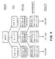
- test sequence is also laid out by the engineer in a hierarchical format.
- the levels of the hierarchy are shown in Figure 4, and each can have a corresponding worksheet to define the test sequence.
- FIG. 5 illustrates an example of a worksheet that is marked to identify the particular dice in the wafer that are to be tested.
- the outline of all of the dice is indicated by the solid line 36, and the individual dice are defined by the dotted-line squares within this outline.
- the selection of the dice to be tested can be indicated by placing an "X" or similar checkmark within each desired die on the worksheet. In such a case, the dice would be sequentially tested in a predetermined pattern.
- the wafer prober might start with the die in the upper right-hand corner of the wafer, proceed horizontally across the row, step down to the next row, and continue along such a path, stopping at each selected die in order as it is reached.
- test shell approach of the present invention offers a much greater degree of flexibility in the die test sequence, however.
- the dice can be tested in any random order. As shown in Figure 5, each selected die to be tested can be sequentially numbered in accordance with any desired test pattern. Thus, it is possible to begin the test procedure with dice in the center of the wafer, and then proceed to other dice located at the periphery of the wafer, for example.
- each type of measurement can be assigned an arbitrary name by the device engineer, and the devices to which each such measurement is to be applied can be indicated on a suitable worksheet.
- FIG. 6 An example of such a worksheet is shown in Figure 6.
- the labels of all devices to be tested are listed in a column 38 along the left-hand side of the worksheet. These labels are preferably specific to a single device on each die.
- a row 40 along the top of the worksheet contains the name of each different type of measurement to be performed, e.g. gate leakage, drain current, etc.
- the application of a particular measurement to a specific device can thereby be easily identified by placing an "X" at the appropriate location in the matrix 42 defined by the worksheet.
- the engineer also selects the order of test using this matrix.
- the specified tests, designated by "X" are processed top left to bottom right by rows. All tests on the first device in the top row are performed before proceeding to the next device.
- Another worksheet can be used to describe the particular test conditions for each named measurement, as well as to assign a label to the results from each measurement.
- one or more suitable measurement algorithms can be chosen from the measurement algorithm library 22 to perform that identified measurement.
- parameters for the measurement such as voltage levels, can be specified. In a preferred implementation of the invention, these parameters can be specified in any one of three forms. First, each might be simply listed as a fixed, numerical value. Secondly, a parameter can be assigned a name which is given a numeric value based upon user defined constants or variables which are given values by the user at the time of test execution, or as a result of a prior measurement performed on the wafer.
- the parameter can be specified as an arithmetic expression defined in terms of fixed numerical values and/or named values as noted above.
- the programming approach of the present invention facilitates parameter passing, i.e. the use of the result from one test as an input condition to a subsequent test within the same test sequence.
- the user can identify the particular output results that are to be included in any desired report, as well as specify the destination for the report, e.g. video screen or printer. Once the user has entered all of this information onto the appropriate worksheets/screens it is stored in corresponding files in the configuration file library 20.
- the measurement algorithm library 22 contains software subroutines which perform specific measurements on test device structures by controlling the instrumentation 10 of the test system. Each subroutine can perform a specific type of measurement. These measurements are not unique to an individual device on a wafer that is being tested, however. Rather, each measurement algorithm is a standardized procedure for a generic but user definable class of device. The characteristics of an individual device under test, as it relates to the class of devices, is provided by the general test program 24 during the test procedure, from information read from the configuration file library 20.
- An example of a class of device is a gated two-terminal diode which is defined as a diode structure having a top electrode, a bottom electrode and a gate terminal.
- the definition of the class may also include provisions for a substrate terminal and a wafer chuck terminal.
- the device can also be described in terms of certain variables.
- the gated two terminal diode can be described in terms of the area of the diode junction, the length of the junction perimeter, the area of the gate, the length of the gate perimeter, the amount of overlap of the diode junction by the gate, the type of dopant, i.e. p or n, used for the top diode electrode and the type of gate.
- the general test program When a test is being run on a specific device in this generic class, the general test program utilizes the information stored in the configuration file library to indicate to the measurement algorithm the respective contact pads in a module which are associated with the terminals of the diode, as well as the values for the parameters which describe the diode structure.
- device classes include island isolation structures, line width structures, MOS capacitors and field effect transistors, contact strings, etc. Users may define and add new device class definitions by completing appropriate worksheets/screens.
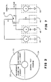
- an FET 44 is a class of device that is defined as having six terminals.
- the gate, drain and source terminals of the device are respectively labeled G, D and S in Figure 7.
- the device is defined as having a bulk terminal B, a substrate terminal and a wafer chuck terminal.
- the measurement algorithm for checking the quality of an FET contains three sets of input variables and one set of output variables.
- One set of input variables to the algorithm comprise information which associates each of these defined terminals of the device to a specific pad in a particular pad pattern.
- reference information stored in the configuration file library 20 indicates the particular pads in a pad pattern that are respectively associated with each of these defined terminals for the device.
- Another set of input variables relate to design characteristics of the device.
- the mask channel width, mask channel length and dopant type of the channel can be stored in the configuration file library 20 and supplied to the measurement algorithm at the time the tests are being carried out on the device.
- the third set of input variables relate to measurement parameters which are assigned specific values by the process engineer. These parameters can include the drain-to-source bias voltage, gate-to-source bias voltages for the "off” and “on” states of the transistor, maximum acceptable drain currents for each of the two states, and bulk-to-source bias voltage. If desired, an integration range can be specified for the ammeter which measures the drain current. The integration range determines the precision of the measurement.
- the output variables for the measurement algorithm can include the drain currents for the "off” and “on” states of the FET, as well as a general indication of the status or quality of the FET based on these other two values.
- the measurement algorithm After defining each of these input and output variables, the measurement algorithm identifies the step-by-step procedure to be carried out to perform the desired measurement.
- a first step in the procedure would be to lower the probe onto the pads of the device, if this step has not been previously performed in connection with another measurement.
- the next step would be to establish the values for various voltage sources, or source measurement units (SMUs), in the measurement instruments 10 and the connections of these units to the pads of the device.
- SMUs source measurement units
- four SMUs are employed in the measurement.
- One SMU 46 is set to a ground reference potential and connected to the source terminal of the device by the relay matrix 12.
- Two other SMUs, 48 and 50 are respectively connected to the gate and drain terminals of the device.
- a fourth SMU 52 is connected in common to each of the bulk, substrate and chuck terminals of the device.
- the values of the latter three SMUs are determined in accordance with the input measurement parameters. More particularly, the voltage of the SMU 48 connected to the drain of the device is determined by the specified drain-to-source input value. Similarly, the voltage output of the SMU 52 connected to the bulk, substrate and chuck terminals is determined by the specified bulk-to-source bias input value.
- the output voltage of the SMU 50 connected to the gate of the device is first set in accordance with the specified gate-to-source bias voltage for the FET when it is in the "off" state.
- the drain current through the device is measured, and this value is assigned to the corresponding output variable. Then, the value of the SMU 50 is changed in accordance with the specified gate-to-source bias voltage for the FET "on" state and the drain current is again measured. This measured value is assigned to another corresponding output variable for the algorithm.
- Table I illustrates one example of a status code that can be assigned for each of the four possible output conditions: TABLE I I d (off) > I d (off)max I d (on) ⁇ I d (on)min Status No No 0 Yes No 1 No Yes 2 Yes Yes 3 where I d (off) is the measured drain current when the transistor is off; I d (on) is the measured drain current when the transistor is on; I d (off)max is the specified maximum drain current when the transistor is off; I d (on)min is the specified minimum drain current when the transistor is on;
- each measurement algorithm can generate one or more control codes in response to the measured parameter to indicate certain types of defects.
- any status code other than zero indicates that the FET is not viable and does not warrant further testing.
- Such a status code can be used to generate another type of output result, labeled a test sequence indicator, which may indicate a defective device.
- Other types of measurement algorithms may return test sequence indicators that indicate a desired change in the testing sequence such as skip to the next measurement, go to the next module or even abort all further tests on the wafer. In response to these indicators, the general test program can terminate all further testing in the measurement, device, module, die or wafer, as the case may be, and move on to the next appropriate structure to be tested.
- test program 24 As indicated in the foregoing, the execution of the test procedure is carried out by the general test program 24.
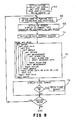
- the basic operation of the program is schematically illustrated in Figure 8, and a flow chart of the major steps in the operation of the program are shown in Figure 9.
- the operator enters a test name as well as other administrative information relating to the test to be carried out.
- the test program obtains all information from the reference information and test definition files stored within the configuration file library 20 that are associated with that particular test. After ensuring that there are no syntax errors or inconsistencies, this information is stored into memory arrays for subsequent access by the program.
- the program proceeds to step 66, where it permits the user to perform run-time editing of parameters and user-defined constants.
- the general test program performs any necessary initialization of the wafer prober and displays alignment information (step 68). For example, if the system is operating in the manual load mode, it may display appropriate diagrams showing where to align the wafer and request the user to indicate when the wafer is properly aligned. If the equipment has automatic loading and alignment capability, the first wafer is aligned automatically and the operator is asked to verify the alignment. All subsequent wafers are loaded and aligned without operator intervention for automatic wafer loaders.
- the general test program initializes the data storage package in step 74. This step initializes the files and communication links necessary to store the results of measurements in a predefined format.
- the general test program proceeds to the probe-and-measure routine 76.
- the program scans the stored configuration file data, determines which tests to perform, moves the prober to the selected location and calls the algorithms to perform the tests.
- the measurement process proceeds in the hierarchical sequence specified in the test definition files without any further interaction on the part of the operator.
- the probe-and-measure routine essentially comprises a set of nested loops, with the loops respectively pertaining to one of the items in the testing hierarchy. More particularly, there is a loop for test pairs, each of which consists of the combination of selected dice (Fig. 5) and a device/measurement set (Fig. 6) specified by the user. Other loops are respectively associated with the die, module, device, measurement and algorithm levels of the hierarchy. An outer loop is provided to cause successive wafers to be sequentially loaded.
- the input variables for the selected algorithm are retrieved and placed in suitable arrays or memory buffers to be sent to the algorithm.
- the algorithm itself is then called and controls the tester's instruments 10 to perform the desired measurements, as explained previously.
- the result data is returned to the general test program. This data is entered into an appropriate cell in the array constructed in step 60.
- the test sequence indicator returned by the algorithm is also checked by the general test program. If the indicator instructs the program to branch out of the normal sequence, for example due to a defective device or module, the appropriate number of loops are exited by the general test program to proceed to the next structure to be tested. This operation is depicted in the flow chart of Figure 10.
- the general test program proceeds in the sequence determined by the test specifications entered by the process engineer on the device/measurement matrix 42 of Figure 6.
- the general test program sequentially accesses the measurement algorithms to carry out the desired tests. If the results of any test return a status code that signifies a defective structure, the test program 24 ignores all further tests for that structure and branches to the test routines for the next selected structure, as explained previously.
- a continuously updated report can be provided on an I/O device such as a CRT screen 54 or printer to inform the user of the most recent measurement results and status information.
- a statistical summary report can be generated on a printer (step 78).
- the general test program can also format and transmit measurement results to a database for off-line data analysis. These reports can be generated at any desired frequency, for example once per die.
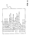
- the procedure for reading the configuration files and building the arrays within program step 60 is shown in greater detail in Figure 11.
- the first six steps involve getting an initial set of reference information and test specification files that pertain to the devices to be tested; remaining files are read as indicated below and in Figure 11.
- the general test program determines which modules are to be tested (step 7), and from this information determines the module reference files that need to be read.
- the program retrieves the first die selection file, determines which measurement algorithms will be required and appends them to the general test program, setting up arrays for the input variables required by each.
- the general test program next proceeds to the allocation of memory space and building of a main array.
- the main array is filled with all of the information that is saved for each tested result.
- the columns of the array can each be assigned to one of the pieces of information that is saved. Some of these pieces of information could be the same of the result, its unit of measure, the value of result itself, statistical analyses of the results over one die or all dice, and sets of limits that are used to determine status codes or test sequence indicators.
- Each row of the array would be assigned to one result and filled as the algorithm relating to that result is carried out.
- the general test program can provide a unique identifier for each test result that is obtained during the testing sequence.
- a unique identifier can be provided is to concatenate the names of the algorithm, its output result, the device and the die.
- the second measurement that is taken with an algorithm ID on a device ABC on a die XYZ could be named ID-Out2-ABC-XYZ.
- the user can be provided with the option to substitute a different (more meaningful) name for the output result portion of the identifier, such as ID-Drain Current-ABC-XYZ.
- test results can be used for subsequent parameter passing in later tests as well as for more informed data analysis.
- a naming convention such as that described above is easily human readable and clearly identifies the source of the test result, independently of the actual testing sequence. In addition, it saves the user from having to develop hundreds of names which might be easily forgotten or which may not clearly identify the result. This capability facilitates the variation of the test sequencing without affecting test results.
- the modular test program approach provided by the present invention offers a number of advantages over the heretofore conventional practice of hard coding an entire test sequence from start to finish in a custom program.
- the approach of the present invention provides for separation of device-under-test descriptions from specific test definitions, and thereby allows numerous engineers to perform different tests on the same type of wafer and/or device without having to repeatedly describe the wafer and device.
- the general test program is the same for every test, it is inherently reused and provides uniformity of function and result in various features such as operator interface, report formats, data format and general test creation process. Further, because there is only a single general test program it is much more robust and easily supported, independent of the ultimate number of tests that it is to be used for.
- the measurement algorithms are modular and generic, they can be reused in any test which requires the particular type of measurement to which each relates. This feature promotes sharing of the program among test system sites. Furthermore, because of their reusability the measurement algorithms promote standardization, which further facilitates testing uniformity. In addition, their modularity and defined input/output protocols for interchange with the general test program promote user creation of additional measurement algorithms.
- the modular and standardized approach of the present invention also provides significant flexibility that enables each test procedure to be optimized. For example, the ability to specify different input parameters for the individual measurement algorithms enables the user to define a single constant to be used as an input variable in a number of measurements within a test. In addition, the result obtained in any measurement can be used as an input variable in subsequent measurements without the need for user interaction between the measurement steps. Furthermore, actual measurement results can be used as a basis for dynamically altering the test sequence, and thereby avoid test steps that are rendered unnecessary once a particular result is obtained.
Landscapes
- Engineering & Computer Science (AREA)
- General Engineering & Computer Science (AREA)
- Physics & Mathematics (AREA)
- General Physics & Mathematics (AREA)
- Computer Hardware Design (AREA)
- Human Computer Interaction (AREA)
- Testing Or Measuring Of Semiconductors Or The Like (AREA)
- Testing Of Individual Semiconductor Devices (AREA)
- Tests Of Electronic Circuits (AREA)
- Testing Electric Properties And Detecting Electric Faults (AREA)
Applications Claiming Priority (2)
| Application Number | Priority Date | Filing Date | Title |
|---|---|---|---|
| US19566788A | 1988-05-18 | 1988-05-18 | |
| US195667 | 1989-05-18 |
Publications (2)
| Publication Number | Publication Date |
|---|---|
| EP0397937A2 true EP0397937A2 (fr) | 1990-11-22 |
| EP0397937A3 EP0397937A3 (fr) | 1991-07-24 |
Family
ID=22722278
Family Applications (1)
| Application Number | Title | Priority Date | Filing Date |
|---|---|---|---|
| EP19890304955 Withdrawn EP0397937A3 (fr) | 1988-05-18 | 1989-05-16 | Système et procédé de commande pour équipement de test paramétrique automatisé |
Country Status (3)
| Country | Link |
|---|---|
| EP (1) | EP0397937A3 (fr) |
| JP (1) | JPH0256947A (fr) |
| KR (1) | KR900019185A (fr) |
Cited By (7)
| Publication number | Priority date | Publication date | Assignee | Title |
|---|---|---|---|---|
| WO1996037839A1 (fr) * | 1995-05-23 | 1996-11-28 | Siemens Aktiengesellschaft | Procede de mesure et de verification assiste par ordinateur de circuits electriques, notamment de modules electroniques, et poste de verification pour la mise en ×uvre dudit procede |
| WO1999014610A1 (fr) * | 1997-09-16 | 1999-03-25 | Teradyne, Inc. | Systeme servant a stocker et a rechercher des donnees nommees de parametres de dispositif dans un systeme d'essai utile pour tester un circuit integre |
| EP1469320A1 (fr) * | 2003-04-15 | 2004-10-20 | Rood Technology Deutschland GmbH + Co | Procédé de génération des commandes de testeur |
| WO2013155348A1 (fr) * | 2012-04-11 | 2013-10-17 | Advantest Corporation | Interposeur entre un dispositif d'essai et un équipement de manipulation de matériel pour séparer et contrôler différentes requêtes de multiples entités lors du fonctionnement d'une cellule de test |
| US9448276B2 (en) | 2012-04-11 | 2016-09-20 | Advantest Corporation | Creation and scheduling of a decision and execution tree of a test cell controller |
| US10371744B2 (en) | 2012-04-11 | 2019-08-06 | Advantest Corporation | Method and apparatus for an efficient framework for testcell development |
| CN116313870A (zh) * | 2023-04-20 | 2023-06-23 | 北海惠科半导体科技有限公司 | 一种晶圆测试方法及装置 |
Families Citing this family (1)
| Publication number | Priority date | Publication date | Assignee | Title |
|---|---|---|---|---|
| JP2725615B2 (ja) * | 1994-10-31 | 1998-03-11 | 日本電気株式会社 | 集積回路試験装置 |
-
1989
- 1989-05-16 EP EP19890304955 patent/EP0397937A3/fr not_active Withdrawn
- 1989-05-17 KR KR1019890006548A patent/KR900019185A/ko not_active Withdrawn
- 1989-05-18 JP JP1125472A patent/JPH0256947A/ja active Pending
Non-Patent Citations (3)
| Title |
|---|
| ELECTRO 1988 CONFERENCE RECORD, vol. 13, 10th - 12th May 1988, pages (45/2) 1-6, Los Angeles, CA, US; S.J. PETERSON et al.: "A high level test program generator for electronics manufacturing test" * |
| ELEKTRONIK, vol. 36, no. 21, October 1987, pages 70-74, Munich, DE; R. WINKLER: "Flexibel testet sich's am besten" * |
| PROCEEDINGS OF THE INTERNATIONAL CONFERENCE ON CIRCUITS AND COMPUTERS, New York, 28th September - 1st October 1982, pages 334-340, IEEE, New York, US; H.D. SCHNURMANN et al.: "A system for testing LSI multi-chip modules using through-the-pins testing" * |
Cited By (10)
| Publication number | Priority date | Publication date | Assignee | Title |
|---|---|---|---|---|
| WO1996037839A1 (fr) * | 1995-05-23 | 1996-11-28 | Siemens Aktiengesellschaft | Procede de mesure et de verification assiste par ordinateur de circuits electriques, notamment de modules electroniques, et poste de verification pour la mise en ×uvre dudit procede |
| AU698573B2 (en) * | 1995-05-23 | 1998-11-05 | Daimlerchrysler Ag | Method for computer-aided measurement and testing of electrical circuits, in particular of electronic assemblies, and a test rig for carrying out the method. |
| WO1999014610A1 (fr) * | 1997-09-16 | 1999-03-25 | Teradyne, Inc. | Systeme servant a stocker et a rechercher des donnees nommees de parametres de dispositif dans un systeme d'essai utile pour tester un circuit integre |
| US6047293A (en) * | 1997-09-16 | 2000-04-04 | Teradyne, Inc. | System for storing and searching named device parameter data in a test system for testing an integrated circuit |
| EP1469320A1 (fr) * | 2003-04-15 | 2004-10-20 | Rood Technology Deutschland GmbH + Co | Procédé de génération des commandes de testeur |
| WO2013155348A1 (fr) * | 2012-04-11 | 2013-10-17 | Advantest Corporation | Interposeur entre un dispositif d'essai et un équipement de manipulation de matériel pour séparer et contrôler différentes requêtes de multiples entités lors du fonctionnement d'une cellule de test |
| US9322874B2 (en) | 2012-04-11 | 2016-04-26 | Advantest Corporation | Interposer between a tester and material handling equipment to separate and control different requests of multiple entities in a test cell operation |
| US9448276B2 (en) | 2012-04-11 | 2016-09-20 | Advantest Corporation | Creation and scheduling of a decision and execution tree of a test cell controller |
| US10371744B2 (en) | 2012-04-11 | 2019-08-06 | Advantest Corporation | Method and apparatus for an efficient framework for testcell development |
| CN116313870A (zh) * | 2023-04-20 | 2023-06-23 | 北海惠科半导体科技有限公司 | 一种晶圆测试方法及装置 |
Also Published As
| Publication number | Publication date |
|---|---|
| EP0397937A3 (fr) | 1991-07-24 |
| KR900019185A (ko) | 1990-12-24 |
| JPH0256947A (ja) | 1990-02-26 |
Similar Documents
| Publication | Publication Date | Title |
|---|---|---|
| US5206582A (en) | Control system for automated parametric test equipment | |
| KR100270652B1 (ko) | 반도체디바이스반송처리장치 | |
| US6223098B1 (en) | Control system for semiconductor integrated circuit test process | |
| US6362013B1 (en) | Semiconductor inspection apparatus and method of specifying attributes of dies on wafer in semiconductor inspection apparatus | |
| US4761607A (en) | Apparatus and method for inspecting semiconductor devices | |
| US5539652A (en) | Method for manufacturing test simulation in electronic circuit design | |
| US5355320A (en) | System for controlling an integrated product process for semiconductor wafers and packages | |
| US5910895A (en) | Low cost, easy to use automatic test system software | |
| US7089139B2 (en) | Method and apparatus for configuration of automated debug of in-circuit tests | |
| US8225152B2 (en) | Method and apparatus for generating electronic test and data structure | |
| EP1012615B1 (fr) | Systeme servant a stocker et a rechercher des donnees nommees de parametres de dispositif dans un systeme d'essai utile pour tester un circuit integre | |
| US6553546B1 (en) | Failure analyzing apparatus and failure analyzing method for semiconductor integrated circuit | |
| US7441168B2 (en) | Fault detecting method and layout method for semiconductor integrated circuit | |
| JPH0815172B2 (ja) | 電子ビームテストプローブ方法及び装置 | |
| US6639417B2 (en) | Semiconductor parametric testing apparatus | |
| EP1756606B1 (fr) | Systeme de support d'etalonnage et de diagnostics dans un systeme de test d'architecture ouverte | |
| EP0397937A2 (fr) | Système et procédé de commande pour équipement de test paramétrique automatisé | |
| US7050921B2 (en) | Electronic test program with run selection | |
| JPH0574909A (ja) | ウエハテスト方法 | |
| US7319935B2 (en) | System and method for analyzing electrical failure data | |
| KR102274522B1 (ko) | 반도체 칩의 테스트 제어 방법 | |
| JP2001015563A (ja) | 検査結果表示方法、検査結果表示装置及び記録媒体 | |
| JP2002016118A (ja) | 半導体パラメトリック試験装置 | |
| KR0167598B1 (ko) | 반도체 웨이퍼 검사 장치 및 그 방법 | |
| JP2657298B2 (ja) | 半導体ウエハの検査方法 |
Legal Events
| Date | Code | Title | Description |
|---|---|---|---|
| PUAI | Public reference made under article 153(3) epc to a published international application that has entered the european phase |
Free format text: ORIGINAL CODE: 0009012 |
|
| AK | Designated contracting states |
Kind code of ref document: A2 Designated state(s): DE FR NL |
|
| PUAL | Search report despatched |
Free format text: ORIGINAL CODE: 0009013 |
|
| AK | Designated contracting states |
Kind code of ref document: A3 Designated state(s): DE FR NL |
|
| 17P | Request for examination filed |
Effective date: 19911026 |
|
| 17Q | First examination report despatched |
Effective date: 19930107 |
|
| STAA | Information on the status of an ep patent application or granted ep patent |
Free format text: STATUS: THE APPLICATION IS DEEMED TO BE WITHDRAWN |
|
| 18D | Application deemed to be withdrawn |
Effective date: 19960220 |