EP0398245A2 - Direktzugriffsspeicher vom dynamischen Typ - Google Patents
Direktzugriffsspeicher vom dynamischen Typ Download PDFInfo
- Publication number
- EP0398245A2 EP0398245A2 EP90109123A EP90109123A EP0398245A2 EP 0398245 A2 EP0398245 A2 EP 0398245A2 EP 90109123 A EP90109123 A EP 90109123A EP 90109123 A EP90109123 A EP 90109123A EP 0398245 A2 EP0398245 A2 EP 0398245A2
- Authority
- EP
- European Patent Office
- Prior art keywords
- bit line
- potential
- line pair
- charge transfer
- sense
- Prior art date
- Legal status (The legal status is an assumption and is not a legal conclusion. Google has not performed a legal analysis and makes no representation as to the accuracy of the status listed.)
- Granted
Links
Images





Classifications
-
- G—PHYSICS
- G11—INFORMATION STORAGE
- G11C—STATIC STORES
- G11C11/00—Digital stores characterised by the use of particular electric or magnetic storage elements; Storage elements therefor
- G11C11/21—Digital stores characterised by the use of particular electric or magnetic storage elements; Storage elements therefor using electric elements
- G11C11/34—Digital stores characterised by the use of particular electric or magnetic storage elements; Storage elements therefor using electric elements using semiconductor devices
- G11C11/40—Digital stores characterised by the use of particular electric or magnetic storage elements; Storage elements therefor using electric elements using semiconductor devices using transistors
- G11C11/401—Digital stores characterised by the use of particular electric or magnetic storage elements; Storage elements therefor using electric elements using semiconductor devices using transistors forming cells needing refreshing or charge regeneration, i.e. dynamic cells
- G11C11/4063—Auxiliary circuits, e.g. for addressing, decoding, driving, writing, sensing or timing
- G11C11/407—Auxiliary circuits, e.g. for addressing, decoding, driving, writing, sensing or timing for memory cells of the field-effect type
-
- G—PHYSICS
- G11—INFORMATION STORAGE
- G11C—STATIC STORES
- G11C11/00—Digital stores characterised by the use of particular electric or magnetic storage elements; Storage elements therefor
- G11C11/21—Digital stores characterised by the use of particular electric or magnetic storage elements; Storage elements therefor using electric elements
- G11C11/34—Digital stores characterised by the use of particular electric or magnetic storage elements; Storage elements therefor using electric elements using semiconductor devices
- G11C11/40—Digital stores characterised by the use of particular electric or magnetic storage elements; Storage elements therefor using electric elements using semiconductor devices using transistors
- G11C11/401—Digital stores characterised by the use of particular electric or magnetic storage elements; Storage elements therefor using electric elements using semiconductor devices using transistors forming cells needing refreshing or charge regeneration, i.e. dynamic cells
- G11C11/4063—Auxiliary circuits, e.g. for addressing, decoding, driving, writing, sensing or timing
- G11C11/407—Auxiliary circuits, e.g. for addressing, decoding, driving, writing, sensing or timing for memory cells of the field-effect type
- G11C11/409—Read-write [R-W] circuits
- G11C11/4091—Sense or sense/refresh amplifiers, or associated sense circuitry, e.g. for coupled bit-line precharging, equalising or isolating
-
- G—PHYSICS
- G11—INFORMATION STORAGE
- G11C—STATIC STORES
- G11C11/00—Digital stores characterised by the use of particular electric or magnetic storage elements; Storage elements therefor
- G11C11/21—Digital stores characterised by the use of particular electric or magnetic storage elements; Storage elements therefor using electric elements
- G11C11/34—Digital stores characterised by the use of particular electric or magnetic storage elements; Storage elements therefor using electric elements using semiconductor devices
- G11C11/40—Digital stores characterised by the use of particular electric or magnetic storage elements; Storage elements therefor using electric elements using semiconductor devices using transistors
- G11C11/401—Digital stores characterised by the use of particular electric or magnetic storage elements; Storage elements therefor using electric elements using semiconductor devices using transistors forming cells needing refreshing or charge regeneration, i.e. dynamic cells
- G11C11/4063—Auxiliary circuits, e.g. for addressing, decoding, driving, writing, sensing or timing
- G11C11/407—Auxiliary circuits, e.g. for addressing, decoding, driving, writing, sensing or timing for memory cells of the field-effect type
- G11C11/409—Read-write [R-W] circuits
- G11C11/4094—Bit-line management or control circuits
Definitions
- the present invention relates to a dynamic type random-access memory having a charge transfer circuit between a bit line pair and a bit line sense amplifier.
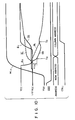
- the potential of the first sense node SN is decreased to be smaller than (V CC /2) - V TN (i.e., the potential difference between the potential of the first sense node SN and the level of the signal ⁇ T is increased to be larger than V TN )
- an impedance of the charge transfer transistor NT1 is gradually decreased in accordance with the potential difference between the two terminals. Therefore, the n-channel sense amplifier NA starts reducing the charge of the first bit line BL, and the potential of the first bit line BL is decreased. As a result, the charge of the first bit line BL starts flowing into the first sense node SN to abruptly reduce a potential decrease speed of the first sense node SN.
- a signal CAS is enabled to decode the column address, and the column selection transistors CT1 and CT2 are turned by a column decode signal CSL i .
- the potentials of the pair of sense nodes SN and SN of the n-channel sense amplifier NA are reamplified by the data buffer DQB via the data lines DQ1 and DQ2 and output from a pair of data buses DL1 and DL2, respectively.
- the signal ⁇ T is returned to the potential V CC to turn on the charge transfer transistors NT1 and NT2.
- the transistor NT1 When the transistor NT1 is turned on, potential redistribution is abruptly performed between the first sense node SN and the first bit line BL, and the potential of the first sense node SN having a smaller capacitance is slightly increased. Since, however, the potentials of the first sense node SN and the first bit line BL are already close to each other, the potential of the first sense node SN is not so abruptly, largely increased.
- bit line precharge dummy cell write signal EQL goes to the potential V CC to precharge the bit lines BL and BL to V BL and dummy cells DC0 and DC1 to a potential V DC .
- the data buffer DQB can correctly perform reamplification.
- the potentials are set to satisfy the relation of V TN ⁇ V M ⁇ V BL + V TN .
- the same effects as those of the above embodiment, however, can be obtained by turning off the charge transfer transistors NT1 and NT2 in an initial stage of the sense operation by the sense amplifier NA and turning on the transistors NT1 and NT2 before the sense amplifier NA completes the sense operation.
- the level of the charge transfer transistor drive signal ⁇ T is increased not to a potential V CC but to a medium potential V M when the charge transfer transistors PT1 and PT2 are to be turned off and is decreased to a potential V SS when the transistors PT1 and PT2 are to be turned on.
- a bit line precharge potential is V BL
- a threshold voltage of the p-channel charge transfer transistors PT1 and PT2 is V TP
- the medium potential VM satisfies a relation of V BL -
- an element having an impedance which changes in accordance with a potential difference between two terminals and being turned off in accordance with a potential difference between a third terminal and one of the two terminals, is connected between a terminal at a bit line side and a terminal at a bit line sense amplifier side, and is temporarily turned off when a small potential difference is produced between the bit lines BL and BL .
- This element is turned off in an initial stage of enabling of the bit line sense amplifier to disconnect the sense nodes SN and SN from the bit lines BL and BL .
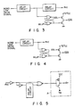
- Figs. 13A and 13B show modifications of the above charge transfer circuit.
- a diode D consisting of a bipolar npn transistor in which a collector and a base are connected is connected between two terminals.
- This diode D is connected in parallel with a switch circuit S, and the switch circuit S is switching-controlled.
- the switch circuit S is turned off in an initial stage of enabling of the bit line sense amplifier, the diode D is turned off.
Landscapes
- Engineering & Computer Science (AREA)
- Microelectronics & Electronic Packaging (AREA)
- Computer Hardware Design (AREA)
- Dram (AREA)
Applications Claiming Priority (2)
| Application Number | Priority Date | Filing Date | Title |
|---|---|---|---|
| JP121204/89 | 1989-05-15 | ||
| JP1121204A JPH0762955B2 (ja) | 1989-05-15 | 1989-05-15 | ダイナミック型ランダムアクセスメモリ |
Publications (3)
| Publication Number | Publication Date |
|---|---|
| EP0398245A2 true EP0398245A2 (de) | 1990-11-22 |
| EP0398245A3 EP0398245A3 (de) | 1992-07-01 |
| EP0398245B1 EP0398245B1 (de) | 1996-07-24 |
Family
ID=14805444
Family Applications (1)
| Application Number | Title | Priority Date | Filing Date |
|---|---|---|---|
| EP90109123A Expired - Lifetime EP0398245B1 (de) | 1989-05-15 | 1990-05-15 | Direktzugriffsspeicher vom dynamischen Typ |
Country Status (5)
| Country | Link |
|---|---|
| US (1) | US5091885A (de) |
| EP (1) | EP0398245B1 (de) |
| JP (1) | JPH0762955B2 (de) |
| KR (1) | KR970001340B1 (de) |
| DE (1) | DE69027886T2 (de) |
Cited By (4)
| Publication number | Priority date | Publication date | Assignee | Title |
|---|---|---|---|---|
| EP0663667A3 (de) * | 1994-01-12 | 1995-10-25 | Siemens Ag | Integrierte Halbleiterspeicherschaltung und Verfahren zu ihrem Betrieb. |
| GB2302973A (en) * | 1995-06-30 | 1997-02-05 | Hyundai Electronics Ind | Data bus drive circuit for a semiconductor memory |
| GB2306027A (en) * | 1995-10-04 | 1997-04-23 | Samsung Electronics Co Ltd | Fast data transmission circuits for semiconductor memory devices |
| CN1038005C (zh) * | 1993-09-10 | 1998-04-08 | 株式会社东芝 | 半导体存储装置 |
Families Citing this family (20)
| Publication number | Priority date | Publication date | Assignee | Title |
|---|---|---|---|---|
| GB9007789D0 (en) | 1990-04-06 | 1990-06-06 | Foss Richard C | Method for dram sensing current control |
| GB9007788D0 (en) * | 1990-04-06 | 1990-06-06 | Foss Richard C | Dynamic memory bitline precharge scheme |
| USRE40552E1 (en) | 1990-04-06 | 2008-10-28 | Mosaid Technologies, Inc. | Dynamic random access memory using imperfect isolating transistors |
| JPH0834257B2 (ja) * | 1990-04-20 | 1996-03-29 | 株式会社東芝 | 半導体メモリセル |
| JPH07122989B2 (ja) * | 1990-06-27 | 1995-12-25 | 株式会社東芝 | 半導体記憶装置 |
| JPH0492287A (ja) * | 1990-08-08 | 1992-03-25 | Internatl Business Mach Corp <Ibm> | ダイナミック・ランダム・アクセス・メモリ |
| JP2564046B2 (ja) * | 1991-02-13 | 1996-12-18 | 株式会社東芝 | 半導体記憶装置 |
| DE69222793T2 (de) * | 1991-03-14 | 1998-03-12 | Toshiba Kawasaki Kk | Halbleiterspeicheranordnung |
| JP3279615B2 (ja) * | 1991-04-15 | 2002-04-30 | 株式会社日立製作所 | 半導体装置 |
| KR950014248B1 (ko) * | 1991-04-19 | 1995-11-23 | 마쯔시다덴기산교 가부시기가이샤 | 다이나믹 ram의 판독/기록회로 |
| JP3181311B2 (ja) * | 1991-05-29 | 2001-07-03 | 株式会社東芝 | 半導体記憶装置 |
| JP2748744B2 (ja) * | 1991-10-01 | 1998-05-13 | 日本電気株式会社 | 半導体記憶装置 |
| JP3464803B2 (ja) * | 1991-11-27 | 2003-11-10 | 株式会社東芝 | 半導体メモリセル |
| KR950009234B1 (ko) * | 1992-02-19 | 1995-08-18 | 삼성전자주식회사 | 반도체 메모리장치의 비트라인 분리클럭 발생장치 |
| DE59407878D1 (de) * | 1994-01-12 | 1999-04-08 | Siemens Ag | Integrierte Halbleiterspeicherschaltung und Verfahren zu ihrem Betrieb |
| KR100264075B1 (ko) | 1997-06-20 | 2000-08-16 | 김영환 | 전하 증폭 비트 라인 센스 앰프 |
| JP2000231791A (ja) * | 1998-12-10 | 2000-08-22 | Fujitsu Ltd | 半導体記憶装置及びデータバスのリセット方法 |
| US6522592B2 (en) * | 2001-04-19 | 2003-02-18 | Micron Technology, Inc. | Sense amplifier for reduction of access device leakage |
| JP2005322380A (ja) * | 2004-04-09 | 2005-11-17 | Toshiba Corp | 半導体記憶装置 |
| KR100765653B1 (ko) | 2006-07-10 | 2007-10-10 | 현대자동차주식회사 | 자동차용 글래스 안테나 잭 |
Family Cites Families (4)
| Publication number | Priority date | Publication date | Assignee | Title |
|---|---|---|---|---|
| US4061999A (en) * | 1975-12-29 | 1977-12-06 | Mostek Corporation | Dynamic random access memory system |
| DE2712735B1 (de) * | 1977-03-23 | 1978-09-14 | Ibm Deutschland | Lese-/Schreibzugriffschaltung zu Speicherzellen eines Speichers und Verfahren zu ihrem Betrieb |
| KR900004635B1 (ko) * | 1987-06-27 | 1990-06-30 | 삼성반도체통신 주식회사 | 반도체 메모리장치의 충전 및 등화회로 |
| JPS6446288A (en) * | 1987-08-13 | 1989-02-20 | Toshiba Corp | Semiconductor memory device |
-
1989
- 1989-05-15 JP JP1121204A patent/JPH0762955B2/ja not_active Expired - Lifetime
-
1990
- 1990-05-14 KR KR1019900006847A patent/KR970001340B1/ko not_active Expired - Fee Related
- 1990-05-15 EP EP90109123A patent/EP0398245B1/de not_active Expired - Lifetime
- 1990-05-15 DE DE69027886T patent/DE69027886T2/de not_active Expired - Fee Related
- 1990-05-15 US US07/523,663 patent/US5091885A/en not_active Expired - Lifetime
Cited By (7)
| Publication number | Priority date | Publication date | Assignee | Title |
|---|---|---|---|---|
| CN1038005C (zh) * | 1993-09-10 | 1998-04-08 | 株式会社东芝 | 半导体存储装置 |
| EP0663667A3 (de) * | 1994-01-12 | 1995-10-25 | Siemens Ag | Integrierte Halbleiterspeicherschaltung und Verfahren zu ihrem Betrieb. |
| US5574694A (en) * | 1994-01-12 | 1996-11-12 | Siemens Aktiengesellschaft | Integrated semiconductor memory circuit and method for its operation |
| GB2302973A (en) * | 1995-06-30 | 1997-02-05 | Hyundai Electronics Ind | Data bus drive circuit for a semiconductor memory |
| GB2302973B (en) * | 1995-06-30 | 2000-03-01 | Hyundai Electronics Ind | Data bus drive circuit for semiconductor memory device |
| GB2306027A (en) * | 1995-10-04 | 1997-04-23 | Samsung Electronics Co Ltd | Fast data transmission circuits for semiconductor memory devices |
| GB2306027B (en) * | 1995-10-04 | 1997-11-26 | Samsung Electronics Co Ltd | Fast data transmission circuits for semiconductor memory devices |
Also Published As
| Publication number | Publication date |
|---|---|
| EP0398245B1 (de) | 1996-07-24 |
| DE69027886D1 (de) | 1996-08-29 |
| JPH02301096A (ja) | 1990-12-13 |
| EP0398245A3 (de) | 1992-07-01 |
| DE69027886T2 (de) | 1997-01-02 |
| US5091885A (en) | 1992-02-25 |
| KR970001340B1 (ko) | 1997-02-05 |
| JPH0762955B2 (ja) | 1995-07-05 |
| KR900019038A (ko) | 1990-12-22 |
Similar Documents
| Publication | Publication Date | Title |
|---|---|---|
| US5091885A (en) | Dynamic type random-access memory having improved timing characteristics | |
| US4943944A (en) | Semiconductor memory using dynamic ram cells | |
| EP0273639B1 (de) | Halbleiterspeicher mit einer Speicherstruktur mit vielfachen Pegeln | |
| JP3241280B2 (ja) | ダイナミック型半導体記憶装置 | |
| US4222112A (en) | Dynamic RAM organization for reducing peak current | |
| EP0449207B1 (de) | Halbleiterspeicheranordnungen von dynamischem Typus | |
| US4397000A (en) | Output circuit | |
| US5640355A (en) | Semiconductor memory device | |
| US6108254A (en) | Dynamic random access memory having continuous data line equalization except at address transition during data reading | |
| US6320806B1 (en) | Input/output line precharge circuit and semiconductor memory device adopting the same | |
| US5323345A (en) | Semiconductor memory device having read/write circuitry | |
| JP2000021180A (ja) | 内蔵ラッチを備えたダイナミック・センス増幅器 | |
| US6049493A (en) | Semiconductor memory device having a precharge device | |
| EP0617428A1 (de) | Halbleiterspeicheranordnung und Speicher-Initialisierungsverfahren | |
| EP0398244A2 (de) | Direktzugriffsspeicher vom dynamischen Typ | |
| JP2795074B2 (ja) | ダイナミックram | |
| EP1143453B1 (de) | Halbleiter Speichereinrichtung | |
| US5777934A (en) | Semiconductor memory device with variable plate voltage generator | |
| US6067264A (en) | High speed semiconductor memory device | |
| US4710901A (en) | Driving circuit for a shared sense amplifier | |
| US20030174533A1 (en) | Dynamic random access memory (DRAM) and method of operating the same | |
| US4768168A (en) | Memory circuit having an improved writing scheme | |
| US5469392A (en) | Semiconductor memory | |
| JP2698232B2 (ja) | 半導体記憶装置 | |
| US4719597A (en) | Driving circuit for a shared sense amplifier with increased speed clock generation circuit for reading addressed memory cells |
Legal Events
| Date | Code | Title | Description |
|---|---|---|---|
| PUAI | Public reference made under article 153(3) epc to a published international application that has entered the european phase |
Free format text: ORIGINAL CODE: 0009012 |
|
| 17P | Request for examination filed |
Effective date: 19900515 |
|
| AK | Designated contracting states |
Kind code of ref document: A2 Designated state(s): DE FR GB |
|
| PUAL | Search report despatched |
Free format text: ORIGINAL CODE: 0009013 |
|
| AK | Designated contracting states |
Kind code of ref document: A3 Designated state(s): DE FR GB |
|
| 17Q | First examination report despatched |
Effective date: 19940405 |
|
| GRAA | (expected) grant |
Free format text: ORIGINAL CODE: 0009210 |
|
| AK | Designated contracting states |
Kind code of ref document: B1 Designated state(s): DE FR GB |
|
| GRAH | Despatch of communication of intention to grant a patent |
Free format text: ORIGINAL CODE: EPIDOS IGRA |
|
| REF | Corresponds to: |
Ref document number: 69027886 Country of ref document: DE Date of ref document: 19960829 |
|
| ET | Fr: translation filed | ||
| PGFP | Annual fee paid to national office [announced via postgrant information from national office to epo] |
Ref country code: GB Payment date: 19970506 Year of fee payment: 8 |
|
| PGFP | Annual fee paid to national office [announced via postgrant information from national office to epo] |
Ref country code: FR Payment date: 19970513 Year of fee payment: 8 |
|
| PLBE | No opposition filed within time limit |
Free format text: ORIGINAL CODE: 0009261 |
|
| STAA | Information on the status of an ep patent application or granted ep patent |
Free format text: STATUS: NO OPPOSITION FILED WITHIN TIME LIMIT |
|
| 26N | No opposition filed | ||
| PG25 | Lapsed in a contracting state [announced via postgrant information from national office to epo] |
Ref country code: GB Free format text: LAPSE BECAUSE OF NON-PAYMENT OF DUE FEES Effective date: 19980515 |
|
| PG25 | Lapsed in a contracting state [announced via postgrant information from national office to epo] |
Ref country code: FR Free format text: LAPSE BECAUSE OF NON-PAYMENT OF DUE FEES Effective date: 19980531 |
|
| GBPC | Gb: european patent ceased through non-payment of renewal fee |
Effective date: 19980515 |
|
| REG | Reference to a national code |
Ref country code: FR Ref legal event code: ST |
|
| PGFP | Annual fee paid to national office [announced via postgrant information from national office to epo] |
Ref country code: DE Payment date: 20070510 Year of fee payment: 18 |
|
| PG25 | Lapsed in a contracting state [announced via postgrant information from national office to epo] |
Ref country code: DE Free format text: LAPSE BECAUSE OF NON-PAYMENT OF DUE FEES Effective date: 20081202 |