EP0398368A2 - Fokussiereinrichtung und digitale Filter dafür - Google Patents
Fokussiereinrichtung und digitale Filter dafür Download PDFInfo
- Publication number
- EP0398368A2 EP0398368A2 EP90109486A EP90109486A EP0398368A2 EP 0398368 A2 EP0398368 A2 EP 0398368A2 EP 90109486 A EP90109486 A EP 90109486A EP 90109486 A EP90109486 A EP 90109486A EP 0398368 A2 EP0398368 A2 EP 0398368A2
- Authority
- EP
- European Patent Office
- Prior art keywords
- signal
- digital
- digital signal
- sample
- output
- Prior art date
- Legal status (The legal status is an assumption and is not a legal conclusion. Google has not performed a legal analysis and makes no representation as to the accuracy of the status listed.)
- Granted
Links
Images






Classifications
-
- H—ELECTRICITY
- H03—ELECTRONIC CIRCUITRY
- H03H—IMPEDANCE NETWORKS, e.g. RESONANT CIRCUITS; RESONATORS
- H03H17/00—Networks using digital techniques
- H03H17/02—Frequency selective networks
- H03H17/0248—Filters characterised by a particular frequency response or filtering method
- H03H17/026—Averaging filters
-
- H—ELECTRICITY
- H04—ELECTRIC COMMUNICATION TECHNIQUE
- H04N—PICTORIAL COMMUNICATION, e.g. TELEVISION
- H04N23/00—Cameras or camera modules comprising electronic image sensors; Control thereof
- H04N23/60—Control of cameras or camera modules
- H04N23/67—Focus control based on electronic image sensor signals
- H04N23/673—Focus control based on electronic image sensor signals based on contrast or high frequency components of image signals, e.g. hill climbing method
Definitions
- the present invention generally relates to lens focusing systems, such as the lens focusing system of a video camera, and novel digital filters particularly adapted for use with such focusing systems.
- a known video camera auto-focusing system operates on the principle that the frequency components (excluding the DC component) of the video signal are at a maximum when the camera is in focus.
- the frequency components of the video signal, with the exception of the DC component, of the video signal are integrated to yield an evaluation signal and the position of the lens is set to the position at which the evaluation signal reaches a maximum value, whereupon the system is in focus.
- the maximum value of the evaluation signal is detected by comparing sequential evaluation signals to determine whether the evaluation signal is changing from an increasing state to a decreasing state.
- Such a control technique is referred to as peak detecting control.
- Fig. 1 illustrates an example of a conventional auto-focusing circuit of a video camera in accordance with such a system.
- a lens 201 is movable by a drive motor 202.
- An image which is transmitted through the lens 201 is converted to an electrical signal by an image pickup device 203, such as a charge coupled device (CCD).
- An output of the image pickup device 203 is supplied to a signal processing circuit 204 which produces a luminance signal Y therefrom and supplies the luminance signal to a detecting circuit 206 through a filter 205 which passes the frequency components of the luminance signal Y with the exception of any DC component therein.
- An output of the detecting circuit 206 is supplied to an A/D converter 207.
- An output of the A/D converter 207 is supplied to an integrating circuit 208 which is operative to integrate those portions thereof which represent a predetermined area of the image in the camera's viewfinder, thereby to provide an evaluation signal which is then supplied to a controller 210.
- the controller 210 controls a drive signal provided to the drive motor 202 by a driver circuit 211 to adjust the position of the lens 201 until the evaluation signal output from the integrating circuit 208 reaches a maximum. To do so, the controller 210 employs a peak detecting control technique, as described hereinbelow.
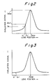
- An exemplary relationship between lens position and the resulting evaluation signal is indicated by the curve provided in Fig. 2.
- the evaluation signal Dn which is obtained at the position l n is compared with an evaluation signal D n+1 which is obtained at the subsequent position l n+1 .
- the lens 201 is moved until the evaluation signal D n which is obtained at a prior lens position l n is larger than the evaluation signal D n+1 which is obtained at a lens position l n+1 which is achieved subsequent to the position l n .
- the evaluation signal increases until the lens has passed a lens position l focus at which the evaluation signal reaches a maximum value D max .
- the evaluation signal begins to decrease.
- the peak detecting control technique determines when the evaluation signals D n and D n+1 at two sequential lens positions l n and l n+1 change from an increasing state to a decreasing state while moving the lens position in a given direction. In such manner, it can be determined that the lens has reached the lens position l focus at which the evaluation signal reaches its maximum value D max , so that an in-focus position is attained.
- a third order analog Chebyshev approximated filter has been used as the filter 205 to eliminate the DC component from the video signal in the conventional signal auto-focusing circuit.
- Fig. 3 illustrates evaluation signal characteristics of the conventional auto-focusing circuit using such an analog filter.
- the inclination of the characteristic curve of the evaluation signal is not constant.
- the inclination of the characteristic curve is nearly eliminated. Accordingly, as shown in Fig. 3, in the case where the initial position of the lens is far from the in-focus position, for example, at the location l p , the difference between the evaluation signal at the lens position l p and the evaluation signal at a lens position l p+1 which is close to the lens position l p is very small, so that it is difficult under these conditions to achieve an in-focus state.
- the overall gain of the circuit may be increased to increase the inclination of the evaluation signal curve when the initial location of the lens is far from the in-focus position.
- a wide dynamic range is then required which is difficult to implement.
- Another object of the invention is to provide an improved focusing apparatus for a lens system utilizing peak detecting control means which need not possess a wide dynamic range.
- a system for providing a focusing signal for use with a lens system having a lens adapted to be positioned for focusing an image transmitted therethrough comprises image pickup means for converting an image from the lens into video signals; and signal filtering means for producing the focusing signal based on the video signal by substantially eliminating from the video signal low frequency components thereof which represent components of the image produced by the lens system when it is out of focus.
- a digital signal filter for filtering a digital input signal comprises means for producing a first digital signal proportional to a difference between the digital input signal and a preceding value of the digital input signal delayed in time by (2m+1) sample periods with respect to the digital input signal, where (m) is an integer; means for integrating the first digital signal to produce a second digital signal; means for producing a third digital signal proportional to a value of the digital input signal delayed in time by (m) sample periods with respect to the digital input signal and multiplied by a coefficient (2m+1); and means for adding the second digital signal and the third digital signal to produce a filtered digital output signal.
- a digital filter for filtering a digital input signal comprises means for producing a first digital signal proportional to a difference between the digital input signal and a preceding value of the digital input signal delayed in time by (2m+1) sample periods with respect to the digital input signal; means for integrating the first digital signal to produce a second digital signal; means for producing a third digital signal proportional to a value of the second digital signal delayed in time by one sample period; means for producing a fourth digital signal proportional to a value of the digital input signal delayed in time by (m+1) sample periods with respect to the digital input signal and multiplied by a coefficient (2m+1); and adding means for adding the third digital signal and the fourth digital signal to produce a filtered digital output signal.
- a digital signal filter for filtering a digital input signal comprises means for producing a first digital signal proportional to a difference between the digital input signal and a preceding value of the digital input signal delayed in time by (2m) sample periods with respect to the digital signal input, where (m) is an integer; means for integrating the first digital signal to produce a second digital signal; means for producing a third digital signal proportional to (m) times a sum of a value of the digital input signal delayed by (m-1) sample periods and a value of the input digital signal delayed by (m) sample periods; and adding means for adding the second digital signal and the third digital signal to produce a filtered digital output signal.
- a digital signal filter for filtering a digital input signal comprises means for producing a first digital signal proportional to a difference between the digital input signal and a preceding value of the digital input signal delayed in time by (2m) sample periods with respect to the digital input signal, where (m) is an integer; means for integrating the first digital signal to produce a second digital signal; means for producing a third digital signal proportional to a value of the second digital signal delayed in time by one sample period; means for producing a fourth digital signal proportional to a sum of a value of the digital input signal delayed by (m+1) sample periods multiplied by a coefficient (m) and a value of the digital input signal delayed by (m) sample periods multiplied by a coefficient (m); and adding means for adding the third digital signal and fourth digital signal to produce a filtered digital output signal.
- a focusing system in accordance with an embodiment of the present invention is there illustrated in which a lens 1 for focusing an image is movable with respect to a CCD image pickup device 3 by means of a drive motor 2.
- An optical image transmitted through the lens 1 is incident on image pickup device 3 which is operative to produce a corresponding electrical signal at an output thereof.
- the output of the CCD image pickup device 3 is supplied to a signal processing circuit 4 which produces a luminance signal Y therefrom.
- the luminance signal Y is supplied to an A/D converter 5 which converts it to a digital signal which is then supplied to a filter circuit 6.
- the filter circuit 6 comprises an out-of-focus approximating low pass filter 7 and a subtracting circuit 8.
- the out-of-focus approximating low pass filter 7 has a transfer characteristic which approximates that of a lens system which is out-of-focus so that an image passing therethrough loses its high frequency components. Accordingly, low pass filter 7 is operative to attenuate the high frequency components of the luminance signal Y to produce a low pass filtered signal representing components of the optical image incident on image pickup device 3 when the lens 1 is positioned such that is is out of focus.
- the output of the low pass filter 7 is subtracted from the luminance signal Y by the subtracting circuit 8, the low frequency components representing the image components present when lens 1 is out of focus are substantially eliminated from the luminance signal Y.
- An output signal from the filter circuit 6 is supplied to a detecting circuit 9 which detects the level of said output signal and provides a corresponding detection output signal to an integrating circuit 10 which is operative to integrate those portions of such detection output signal corresponding to a predetermined area of the optical image incident on the image pickup device 3.
- An output of the integrating circuit 10 is an evaluation signal which is supplied to a controller 11.
- the driver 12 is operative to supply power to the drive motor 2 based on a control signal from the controller 11 determined by the evaluation signal from the integrating circuit 10.
- the controller 11 adjusts the position of the lens 1 to that at which the evaluation signal output from the integrating circuit 10 reaches a maximum.
- the controller 11 utilizes a peak detecting control technique according to which, when the lens 1 is moved in one direction, the evaluation signals at sequential lens positions are compared to thereby detect the lens position at which the evaluation signals change from an increasing state to a decreasing state, thereby indicating that the system is in focus.
- a desired characteristic curve is shown in Fig. 5 wherein the abscissa denotes lens position, the ordinate indicates the corresponding evaluation signal level and l f represents an in-focus position of the lens.
- the out-of-focus approximating low pass filter 7 of the filter circuit 6 advantageously comprises a digital averaging low pass filter, but it will be appreciated that the filter 7 may take other forms as well.
- the characteristic curve of the resulting evaluation signal approaches an ideal curve as shown in Fig. 5, that is the characteristic curve is one in which the inclination is almost constant.
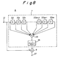
- the out-of-focus approximating low pass filter 7 of the filter circuit 6 is illustrated as an N stage (2m) digital low pass filter.
- a transfer function H(z) of the N stage (2m) digital low pass filter 7 may be expressed as:
- the averaging low pass filter 7 implements the above transfer function of equation (1), while eliminating the group delay correction factor z m .
- one-sample long delay circuits 221 to 22 2m totalling 2m stages are cascade connected, where (m) is an integer.
- An input terminal 21 is provided at one end of the cascade connection.
- Outputs from the delay circuits 221 to 22 2m are supplied as inputs to an adding circuit 23.
- An output signal from the adding circuit 23 is supplied to a multiplying circuit 24 which is operative to multiply the signal by a factor (1/(2m + 1)), and to supply the multiplied signal to an output terminal 25 of the multiplying circuit 24.
- the filter circuit 6 of Fig. 4 includes the digital averaging low pass filter 7 shown in Fig. 6, such filter circuit 6 may be completed simply by subtractively combining the input and output signals of the filter 7. More specifically, in the filter circuit 6 of Fig. 8, a signal from the input terminal 21 of filter 7 is supplied to a noninverting input terminal of the subtracting circuit 8 and to the input of the filter circuit 7 whose output is supplied to an inverting input terminal of the subtracting circuit 8. Accordingly, the subtracting circuit 8 subtracts an output signal of the low pass filter 7 from the signal supplied to input terminal 21, and an output of the subtracting circuit 8 is supplied to an output terminal 27 of the filter circuit 6.
- a relatively less complex high pass filter suitable for use as the filter circuit 6 of Fig. 4 may be obtained by implementing a transfer function derived by subtracting the terms on the right side of equation (1) from 1, as follows
- a high pass filter 30 is illustrated therein which implements the transfer function of equation (3) and in one advantageous embodiment is substituted for the filter circuit 6 of the focusing system illustrated in Fig. 4.
- a digital signal from an input terminal 31 is supplied to an m-sample long delay circuit 32 as well as to a (2m + 1) sample long delay circuit 33 and a noninverting input of a subtracting circuit 34.
- An output of the (2m + 1) sample long delay circuit 33 is supplied to an inverting input of the subtracting circuit 34.
- An output of the subtracting circuit 34 is supplied to a first input of an adding circuit 35.
- An output of the adding circuit 35 is supplied to an inverting input of a subtracting circuit 36 and is also fed back to a second input of the adding circuit 35 through a one-sample long delay circuit 37. Accordingly, adding circuit 35 and delay circuit 37 together serve to integrate the signal supplied to the first input of the adding circuit 35.
- An output of the m-sample long delay circuit 32 is supplied to an input of a (2m + 1) multiplying circuit 38.
- An output of the (2m + 1) multiplying circuit 38 is supplied to a noninverting input of the subtracting circuit 36.
- An output of the subtracting circuit 36 is supplied to an input of a (1/(2m + 1)) multiplying circuit 39 which provides an output signal to an output terminal 40 of the filter 30.
- a solid line indicates amplitude characteristics and a broken line represents phase characteristics.
- a further, simplified embodiment of a high pass filter is illustrated in the form of a filter 50 comprising an m-sample long delay circuit 52 and an (m + 1) sample long delay circuit 53 which are cascade connected.
- An input digital signal from an input terminal 51 of the filter is supplied to the input of delay circuit 52 and to a noninverting input of a subtracting circuit 54.
- the output of delay circuit 53 is supplied to an inverting input of the subtracting circuit 54.
- An output from the m-sample long delay circuit 52 is supplied to a first input of an adding circuit 56 and to the input of a multiplying circuit 55 which is operative to multiply the input signal by a coefficient (2m).
- the 2m-multiplying circuit 55 comprises a bit shift circuit.
- An output of the multiplying circuit 55 is supplied to a second input of the adding circuit 56.
- An output of the adding circuit 56 is supplied to a non-inverting input of a subtracting circuit 58.
- An output of the subtracting circuit 54 is supplied to a first input of an adding circuit 57.
- An output of the adding circuit 57 is supplied to an inverting input of the subtracting circuit 58 and also is fed back to a second input of the adding circuit 57 through a one-sample long delay circuit 59, so that adding circuit 57 and delay circuit 59 together act as an integrator.
- Registers (not shown for purposes of simplicity and clarity) are provided for latching the outputs of subtracting circuit 54 and adding circuits 56 and 57.
- An output of the subtracting circuit 58 is provided to an output terminal 60 of the filter 50.
- the filter 50 of Fig. 11 is relatively less complex than the filter 30 of Fig. 9 and is better adapted for achieving high speed operation.
- the filter 50 of the Fig. 11 embodiment does not require the (1/(2m +1)), multiplier 39, since it merely affects the overall gain factor of the circuit 30.
- the multiplying circuit 38 unlike the multiplying circuit 39, the multiplying circuit 38, however, is positioned in only on branch of the filter 30. Multipliers are relatively complex circuits and tend to have low operating speeds. Nevertheless, the filter 50 of Fig. 11 achieves improved operating speed and reduced circuit complexity by achieving the (2m + 1) multiplying of circuit 38 through the combination of a 2m-bit shifting circuit 55 and an adding circuit 56.
- the (2m + 1) sample long delay circuit 33 of the filter 30 is replaced in the filter 50 by the cascade connection of the m-sample long delay circuit 52 and the (m + 1) sample long delay circuit 53. Accordingly, by supplying an output at the point where the m-sample long delay circuit 52 connects to the (m + 1) sample delay circuit 53, the required input to the (2m + 1) multiplying circuit is provided and the m- sample long delay circuit 32 of the filter 30 is omitted in the filter 50 thereby further simplifying the latter.
- a still further embodiment of a digital high pass filter is illustrated in the form of a filter circuit 75.
- filter circuit 75 an (m + 1) sample long delay circuit 62 and an m-sample long delay circuit 63 are cascade connected.
- An input digital signal from an input terminal 61 is supplied to a noninverting input of a subtracting circuit 64 and is also supplied to an inverting input of the subtracting circuit 64 through the (m + 1) sample long delay circuit 62 and the m-sample long delay circuit 63.
- An output from the (m + 1) sample long delay circuit 62 is supplied to a first input of an adding circuit 66 and to a 2m-multiplying circuit 65 which advantageously comprises a bit shift circuit.
- An output of the multiplying circuit 65 is supplied to a second input of the adding circuit 66.
- An output of the adding circuit 66 is supplied to an input of a one-sample long delay circuit 72 and an output of the one-sample long delay circuit 72 is supplied to a noninverting input terminal of a subtracting circuit 68.
- An output of the subtracting circuit 64 is supplied to an input of a one-sample long delay circuit 71.
- An output of the one-sample long delay circuit 71 is supplied to a first input of an adding circuit 67.
- An output of the adding circuit 67 is supplied to an input of a one-sample long delay circuit 69.
- An output of the one-sample long delay circuit 69 is fed back to a second input of the adding circuit 67 and is also supplied to an inverting input of the subtracting circuit 68 so that adding circuit 67 and delay circuit 69 together act as an integrator.
- An output of the subtracting circuit 68 is provided to an output terminal 70 of the filter circuit 75.
- the filter circuit 75 of Fig. 12 achieves further hardware simplification compared with the filter circuit 50 of Fig. 11.
- registers are employed to latch the outputs of the adding and subtracting circuits.
- the filter circuit 50 there are actually provided, in addition to the components shown on Fig. 11, a one-sample long delay circuit arranged at the output of the subtracting circuit 54, a further one-sample long delay circuit arranged at the output of the adding circuit 56, and a still further one-sample long delay circuit arranged at the output of the adding circuit 57 and which are operative to latch said outputs.
- a further one-sample long delay circuit for delay matching is required at the output of the adding circuit 56.
- the output of the adding circuit 67 is supplied to the one-sample long delay circuit 69 and an output of the one-sample long delay circuit 69 is fed back to the adding circuit 67 and is also supplied to the subtracting circuit 68.
- the operations of delaying and feeding back the output of the adding circuit 57 and latching its output are both provided by a single one-sample long delay circuit 69 and the necessary matching one-sample delay is provided in the (m + 1) sample delay circuit 62.
- the complexity of the Fig. 11 embodiment is further reduced in the embodiment of Fig. 12.
- the filter circuit 75 of the Fig. 12 embodiment is suitable for use in the focusing system of Fig. 4 in place of the filter 6.
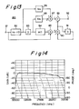
- FIG. 13 yet another embodiment of a high pass filter in accordance with the present invention is illustrated in the form of a filter circuit 80.
- filter circuit 80 an (m - 1) sample long delay circuit 82, a one-sample long delay circuit 83, and an m-sample long delay circuit 84 are cascade connected, in that order.
- An input digital signal applied at an input terminal 81 of the filter circuit 80 is supplied to a noninverting input of a subtracting circuit 85 and, after a (2m) sample long delay, is supplied to an inverting input of the subtracting circuit 85 through the cascade connected (m - 1) sample long delay circuit 82, one-sample long delay circuit 83, and m-sample long delay circuit 84.
- An output from the (m - 1) sample long delay circuit 82 is supplied to a multiplying circuit 86 which is operative to multiply said output by a coefficient (m).
- the multiplying circuit 86 is advantageously comprised of a bit shift circuit.
- An output of the multiplying circuit 86 is supplied to a first input of an adding circuit 87.
- An output from the one-sample delay circuit 83 is supplied to a multiplying circuit 88 which is operative to multiply said output by a coefficient (m).
- the multiplying circuit 88 like the multiplying circuit 86, is advantageously comprised of a bit shift circuit.
- An output of the multiplying circuit 88 is supplied to a second input of the adding circuit 87.
- An output of the adding circuit 87 is supplied to a noninverting input of a subtracting circuit 89.
- An output of the subtracting circuit 85 is supplied to a first input of an adding circuit 90.
- An output of the adding circuit 90 is supplied to an inverting input of the subtracting circuit 89 and is also fed back to a second input of the adding circuit 90 through a one-sample long delay circuit 91, such that adding circuit 90 and delay circuit 91 together act as an integrator.
- Registers (not shown for purposes of simplicity and clarity) are provided for latching the outputs of subtracting circuit 85 and of adding circuits 87 and 90.
- An output of the subtracting circuit 89 is provided to an output terminal 92 of the filter circuit 80.
- a signal multiplied by a factor (2m) and the same signal which has not been multiplied are added by the adding circuits 56 and 66, respectively.
- the circuitry can be further simplified with respect to that of the circuits 50 and 75 of Figs. 11 and 12.
- the high pass filter 80 of Fig. 13 is based on the low pass filter transfer function of H(z) of equation (4), to provide a high pass transfer function by subtracting the right side of equation (4) from 1, as follows:
- the group delay factor z (m-(1/2)) may be ignored since it represents an overall circuit gain.
- This average value represents an estimated signal value occurring at a time intermediate to the two sequential samples used to estimate said average value.
- the embodiment of Fig. 13 implements the approximation of equation (6) by multiplying the outputs of the (m - 1) sample long delay circuit 82 and of the one-sample long delay circuit 83 each by a factor (m) by means of the multiplying circuits 86 and 88, respectively, and then adding the outputs of the multiplying circuits 86 and 88 with the use of the adding circuit 87.
- the word lengths of the outputs from the multiplying circuits 86 and 88 provided as inputs to the adding circuit 87 are nearly equal which simplifies the construction of the adding circuit 87 and it is sufficient to set the word length of the adding circuit 87 to only one bit more than the number of bits in the input data.
- a solid line indicates amplitude characteristics and a broken line represents phase characteristics. It will be seen therein that certain high frequency components are lost.
- the filter circuit 80 may serve in place of the filter circuit 6 in the auto-focusing circuit of Fig. 4.
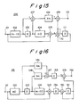
- an (m - 1) sample long delay circuit 102, one sample long delay circuit 103, and an m- sample long delay circuit 104 are cascade connected, in that order.
- An input digital signal from an input terminal 101 of the filter circuit 100 is supplied to a noninverting input of a subtracting circuit 105 and, after a (2m) sample long delay, is also supplied to an inverting input of the subtracting circuit 105 through the (m - 1) sample long delay circuit 102, one-sample long delay circuit 103, and m-sample long delay circuit 104.
- An output of the (m - 1) sample long delay circuit 102 is supplied to one input of an adding circuit 107.
- An output of the one-sample long delay circuit 103 is supplied to a second input of the adding circuit 107.
- An output of the adding circuit 107 is supplied to a multiplying circuit 106 which is operative to multiply said output by a coefficient (m) and is advantageously comprised of a bit shift circuit.
- An output of the multiplying circuit 106 is supplied to the noninverting input of a subtracting circuit 109.
- An output of the subtracting circuit 105 is supplied to a first input of an adding circuit 110.
- An output of the adding circuit 110 is supplied to an inverting input of the subtracting circuit 109 and is also fed back to a second input of the adding circuit 110 through a one sample long delay circuit 111, so that adding circuit 110 and delay circuit 111 together act as an integrator.
- Registers (not shown for purposes of simplicity and clarity) are provided for latching the outputs of subtracting circuit 105 and adding circuit 110.
- An output of the subtracting circuit 109 is provided to an output terminal 112 of the filter circuit 100.
- the operations of the multiplying circuits 86 and 88 of the filter circuit 80 of Fig. 13 are carried out by the multiplying circuit 106, thereby reducing the amount of circuitry required in the circuit 100 over that of circuit 80.
- FIG. 16 yet another embodiment of the present invention is shown in the form of a filter circuit 115.
- filter circuit 115 an m-sample long delay circuit 122, a one-sample long delay circuit 123, and an (m - 1) sample long delay circuit 124 are cascade connected, in that order.
- An input digital signal from an input terminal 121 of the filter circuit 115 is supplied to a noninverting input of a subtracting circuit 125 and, after an m-sample long delay, is also supplied to an inverting input of the subtracting circuit 125 through the m- sample long delay circuit 122, one-sample long delay circuit 123, and (m - 1) sample long delay circuit 124.
- An output of the m-sample long delay circuit 122 is supplied to a multiplying circuit 126 which is operative to multiply said output by a coefficient (m).
- An output of the multiplying circuit 126 is supplied to a first input of an adding circuit 127.
- An output from the one-sample long delay circuit 123 is supplied to a multiplying circuit 128 which is operative to multiply said output by a coefficient (m).
- An output of the multiplying circuit 128 is supplied to a second input of the adding circuit 127.
- An output of the adding circuit 127 is supplied to a one-sample long delay circuit 133 and an output thereof is supplied to a noninverting input of a subtracting circuit 129.
- An output of the subtracting circuit 125 is supplied to a one-sample long delay circuit 134 and an output thereof is supplied to a first input of an adding circuit 130.
- An output of the adding circuit 130 is supplied to an inverting input of the subtracting circuit 129 through a one-sample long delay circuit 131 and is also fed back to a second input of the adding circuit 130, such that adding circuit 130 and delay circuit 131 together act as an integrator.
- An output of the subtracting circuit 129 is provided to an output terminal 132 of the filter circuit 115.
- the filter circuit 115 also may be substituted for the filter circuit 6 of Fig. 4.
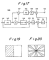
- FIG. 17 yet another embodiment of the present invention is illustrated therein in the form of a filter circuit 140.
- an m-sample long delay circuit 142, a one-sample long delay circuit 143, and an (m - 1) sample long delay circuit 144 are cascade connected, in that order.
- An input digital signal from an input terminal 141 is supplied to a noninverting input of a subtracting circuit 145 and, after a (2m) sample long delay, is also supplied to an inverting input of the subtracting circuit 145 through the m-sample long delay circuit 142, one-sample long delay circuit 143, and (m - 1) sample long delay circuit 144.
- An output of the m-sample long delay circuit 142 is supplied to a first input of an adding circuit 147 and an output of the one-sample long delay circuit 143 is supplied to a second input of the adding circuit 147.
- An output of the adding circuit 147 is supplied to a multiplying circuit 146 which is operative to multiply said output by a coefficient (m).
- An output of the multiplying circuit 146 is supplied to a one-sample long delay circuit 153 and an output thereof is supplied to a noninverting input of a subtracting circuit 149.
- An output of the subtracting circuit 145 is supplied to a one-sample long delay circuit 161 and an output thereof is supplied to a first input of an adding circuit 150.
- An output of the adding circuit 150 is supplied to a one-sample long delay circuit 151.
- An output of the one-sample long delay circuit 151 is supplied to an inverting input of the subtracting circuit 149 and is also fed back to a second input of the adding circuit 150, such that adding circuit 150 and delay circuit 151 together act as an integrator.
- An output of the subtracting circuit 149 is provided to an output terminal 152 of the filter circuit 140.
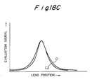
- Figs. 18A to 18C show comparisons of the curves of evaluation signals produced in a conventional auto-focusing circuit in which the evaluation signal is obtained by using an analog high pass filter with curves of evaluation signals obtained in accordance with the present invention.
- Fig. 18A shows evaluation signal characteristics obtained in the case where a doll is used as an object to be imaged.
- A2 identifies a curve of an evaluation signal obtained with the use of a conventional auto-focusing circuit and A1 indicates the curve of an evaluation signal obtained with the use of an auto-focusing circuit in accordance with the present invention.
- Fig. 18B illustrates evaluation signal characteristics obtained in the case where a flat picture whose left side is black and right side is white, as shown in Fig. 19, is used as an object to be imaged.
- B2 denotes a curve of the evaluation signal obtained with the use of a conventional auto-focusing circuit
- B1 indicates a curve of the evaluation signal obtained with the use of an auto-focusing circuit in accordance with the present invention.
- Fig. 18C shows evaluation signal characteristics in the case where a flat picture of radiating pattern, as shown in Fig. 20, is used as an object to be imaged.
- C2 denotes the curve of an evaluation signal obtained with the use of a conventional auto-focusing circuit and C1 indicates the curve of an evaluation signal obtained with the use of an auto-focusing circuit in accordance with the present invention.
- Figs. 18A to 18C the characteristic curves of evaluation signals indicated at A1, B1 and C1 were produced with the use of a filter circuit comprising an out-of-focus function approximating low pass filter and a subtracting circuit in accordance with the present invention. It will be seen that, through the use of the present invention, the inclination of the characteristic curve of the evaluation signal more nearly approaches a constant value and, accordingly, approximates an ideal characteristic curve for implementing an autofocus system of a video camera.
- a filter circuit for extracting predetermined frequency components of a video signal comprising an out-of-focus function approximating low pass filter and a subtracting circuit.
Landscapes
- Engineering & Computer Science (AREA)
- Multimedia (AREA)
- Signal Processing (AREA)
- Physics & Mathematics (AREA)
- Computer Hardware Design (AREA)
- Mathematical Physics (AREA)
- Automatic Focus Adjustment (AREA)
Applications Claiming Priority (4)
| Application Number | Priority Date | Filing Date | Title |
|---|---|---|---|
| JP127560/89 | 1989-05-19 | ||
| JP1127560A JP3041858B2 (ja) | 1989-05-19 | 1989-05-19 | ディジタルハイパスフィルタ |
| JP1135351A JP2946531B2 (ja) | 1989-05-29 | 1989-05-29 | オートフォーカス回路 |
| JP135351/89 | 1989-05-29 |
Publications (3)
| Publication Number | Publication Date |
|---|---|
| EP0398368A2 true EP0398368A2 (de) | 1990-11-22 |
| EP0398368A3 EP0398368A3 (de) | 1991-09-25 |
| EP0398368B1 EP0398368B1 (de) | 1996-07-10 |
Family
ID=26463493
Family Applications (1)
| Application Number | Title | Priority Date | Filing Date |
|---|---|---|---|
| EP90109486A Expired - Lifetime EP0398368B1 (de) | 1989-05-19 | 1990-05-18 | Fokussiereinrichtung und digitale Filter dafür |
Country Status (3)
| Country | Link |
|---|---|
| US (1) | US5070408A (de) |
| EP (1) | EP0398368B1 (de) |
| DE (1) | DE69027711T2 (de) |
Cited By (4)
| Publication number | Priority date | Publication date | Assignee | Title |
|---|---|---|---|---|
| EP0572163A3 (de) * | 1992-05-29 | 1994-01-05 | Sony Corporation | Autofokus-Vorrichtung |
| EP0586047A3 (de) * | 1992-08-27 | 1994-11-17 | Sony Electronics Inc | Automatische Fokussierung für Kameras. |
| WO2005098555A1 (de) * | 2004-04-05 | 2005-10-20 | Siemens Aktiengesellschaft | Motorregelungsvorrichtung und entsprechendes regelungsverfahren |
| DE4143061B4 (de) * | 1990-12-27 | 2010-12-30 | Sony Corp. | Videokamera |
Families Citing this family (4)
| Publication number | Priority date | Publication date | Assignee | Title |
|---|---|---|---|---|
| EP0679021B1 (de) * | 1994-04-19 | 2010-12-15 | Eastman Kodak Company | Kamera mit automatischer Belichtungssteuerung unter Verwendung von CCD-Sensor mit verstellbarem Belichtungsindex |
| JP3298357B2 (ja) | 1995-04-10 | 2002-07-02 | ミノルタ株式会社 | フィルム画像再生装置 |
| JP5900273B2 (ja) * | 2012-10-03 | 2016-04-06 | 株式会社ソシオネクスト | 合焦評価値生成装置、合焦評価値生成方法、及び、合焦評価値生成プログラム |
| CN112312018B (zh) * | 2016-04-15 | 2022-05-17 | 深圳市大疆创新科技有限公司 | 使用自适应步长的对比度检测自动聚焦 |
Family Cites Families (11)
| Publication number | Priority date | Publication date | Assignee | Title |
|---|---|---|---|---|
| DE3121310A1 (de) * | 1981-05-29 | 1982-12-16 | Robert Bosch Gmbh, 7000 Stuttgart | Digitales filter |
| JPS5834615A (ja) * | 1981-08-24 | 1983-03-01 | Victor Co Of Japan Ltd | Iirデイジタルフイルタ |
| US4544953A (en) * | 1983-03-28 | 1985-10-01 | Designs For Vision, Inc. | Automatic facusing using slope and peak detection |
| JPS60182289A (ja) * | 1984-02-29 | 1985-09-17 | Toshiba Corp | デジタルテレビジヨン信号処理回路 |
| JPH0771209B2 (ja) * | 1986-06-13 | 1995-07-31 | 三洋電機株式会社 | オ−トフォ−カス回路 |
| DE3783435T2 (de) * | 1986-10-02 | 1993-07-29 | Victor Company Of Japan | Automatisches fokussierungsverfahren. |
| JP2535845B2 (ja) * | 1986-10-08 | 1996-09-18 | キヤノン株式会社 | 自動合焦装置 |
| US4841370A (en) * | 1986-11-17 | 1989-06-20 | Sanyo Electric Co., Ltd. | Automatic focusing circuit for automatically matching focus in response to video signal |
| US4833541A (en) * | 1987-09-07 | 1989-05-23 | Sanyo Electric Co., Ltd. | Image sensing apparatus having function of automatically matching focus and exposure in response to video signal |
| US4975726A (en) * | 1987-11-25 | 1990-12-04 | Matsushita Electric Industrial Co., Ltd. | Automatic focusing apparatus |
| KR970010204B1 (en) * | 1988-05-11 | 1997-06-23 | Sanyo Electric Co | Image sensing apparatus having automatic focusing function of automatically matching focus in response to video signal |
-
1990
- 1990-05-15 US US07/523,568 patent/US5070408A/en not_active Expired - Lifetime
- 1990-05-18 EP EP90109486A patent/EP0398368B1/de not_active Expired - Lifetime
- 1990-05-18 DE DE69027711T patent/DE69027711T2/de not_active Expired - Fee Related
Cited By (7)
| Publication number | Priority date | Publication date | Assignee | Title |
|---|---|---|---|---|
| DE4143061B4 (de) * | 1990-12-27 | 2010-12-30 | Sony Corp. | Videokamera |
| EP0572163A3 (de) * | 1992-05-29 | 1994-01-05 | Sony Corporation | Autofokus-Vorrichtung |
| US5982430A (en) * | 1992-05-29 | 1999-11-09 | Sony Corporation | Auto focus apparatus |
| EP0586047A3 (de) * | 1992-08-27 | 1994-11-17 | Sony Electronics Inc | Automatische Fokussierung für Kameras. |
| US5539462A (en) * | 1992-08-27 | 1996-07-23 | Sony Corporation | Camera auto focus system with detector circuits for generating evaluation functions |
| WO2005098555A1 (de) * | 2004-04-05 | 2005-10-20 | Siemens Aktiengesellschaft | Motorregelungsvorrichtung und entsprechendes regelungsverfahren |
| US7692397B2 (en) | 2004-04-05 | 2010-04-06 | Siemens Aktiengesellschaft | Motor control device and corresponding control method |
Also Published As
| Publication number | Publication date |
|---|---|
| DE69027711D1 (de) | 1996-08-14 |
| EP0398368B1 (de) | 1996-07-10 |
| US5070408A (en) | 1991-12-03 |
| DE69027711T2 (de) | 1996-12-05 |
| EP0398368A3 (de) | 1991-09-25 |
Similar Documents
| Publication | Publication Date | Title |
|---|---|---|
| US5070353A (en) | Automatic focusing apparatus | |
| US5434615A (en) | Signal processing circuit adaptable to electronic endoscopes having different lengths | |
| EP0169740B1 (de) | Ausgangssignalprozessorschaltung einer Ladungsgekoppelten Anordnung | |
| US4975726A (en) | Automatic focusing apparatus | |
| US5070408A (en) | Focusing apparatus and digital filters for use therewith | |
| EP0860725A3 (de) | Autofokuskamera | |
| KR0184887B1 (ko) | 샘플링 주파수 승환 필터 회로 | |
| US5077613A (en) | Video camera with automatic focusing function | |
| KR950011820B1 (ko) | 디지탈 비데오 신호의 주파수 스펙트럼의 고주파수 부분을 피킹하는 장치 | |
| US5185707A (en) | Focusing apparatus and digital filters for use therewith | |
| US5475427A (en) | Video signal noise suppression circuit | |
| KR100213418B1 (ko) | 비디오 카메라용 포커싱 제어 장치 | |
| US5982430A (en) | Auto focus apparatus | |
| US5003378A (en) | Automatic white balance circuit | |
| US5739858A (en) | Automatic focusing device using a plurality of different frequency components extracted at the same point | |
| US4864407A (en) | Pick up device having pick up elements arranged in a predetermined pattern and smear component reduction varying independence upon the position of a pick up element in the pattern | |
| US4677306A (en) | Drive apparatus for solid-state image pickup device | |
| US4587416A (en) | Focus detecting apparatus for microscope or camera | |
| JP3041858B2 (ja) | ディジタルハイパスフィルタ | |
| KR970004196B1 (ko) | 티브이의 노이즈 제거장치 | |
| JP3279583B2 (ja) | ビデオカメラ | |
| JPS62146081A (ja) | 自動焦点整合装置 | |
| JPH07177415A (ja) | 自動合焦装置 | |
| JP2000028912A (ja) | 自動焦点調節装置 | |
| JP2821231B2 (ja) | 自動合焦装置 |
Legal Events
| Date | Code | Title | Description |
|---|---|---|---|
| PUAI | Public reference made under article 153(3) epc to a published international application that has entered the european phase |
Free format text: ORIGINAL CODE: 0009012 |
|
| AK | Designated contracting states |
Kind code of ref document: A2 Designated state(s): DE FR GB |
|
| PUAL | Search report despatched |
Free format text: ORIGINAL CODE: 0009013 |
|
| AK | Designated contracting states |
Kind code of ref document: A3 Designated state(s): DE FR GB |
|
| 17P | Request for examination filed |
Effective date: 19911204 |
|
| 17Q | First examination report despatched |
Effective date: 19931005 |
|
| GRAH | Despatch of communication of intention to grant a patent |
Free format text: ORIGINAL CODE: EPIDOS IGRA |
|
| GRAH | Despatch of communication of intention to grant a patent |
Free format text: ORIGINAL CODE: EPIDOS IGRA |
|
| GRAA | (expected) grant |
Free format text: ORIGINAL CODE: 0009210 |
|
| AK | Designated contracting states |
Kind code of ref document: B1 Designated state(s): DE FR GB |
|
| REF | Corresponds to: |
Ref document number: 69027711 Country of ref document: DE Date of ref document: 19960814 |
|
| ET | Fr: translation filed | ||
| PLBE | No opposition filed within time limit |
Free format text: ORIGINAL CODE: 0009261 |
|
| STAA | Information on the status of an ep patent application or granted ep patent |
Free format text: STATUS: NO OPPOSITION FILED WITHIN TIME LIMIT |
|
| 26N | No opposition filed | ||
| REG | Reference to a national code |
Ref country code: GB Ref legal event code: IF02 |
|
| PGFP | Annual fee paid to national office [announced via postgrant information from national office to epo] |
Ref country code: DE Payment date: 20080522 Year of fee payment: 19 |
|
| PGFP | Annual fee paid to national office [announced via postgrant information from national office to epo] |
Ref country code: GB Payment date: 20080521 Year of fee payment: 19 |
|
| GBPC | Gb: european patent ceased through non-payment of renewal fee |
Effective date: 20090518 |
|
| REG | Reference to a national code |
Ref country code: FR Ref legal event code: ST Effective date: 20100129 |
|
| PG25 | Lapsed in a contracting state [announced via postgrant information from national office to epo] |
Ref country code: FR Free format text: LAPSE BECAUSE OF NON-PAYMENT OF DUE FEES Effective date: 20090602 |
|
| PGFP | Annual fee paid to national office [announced via postgrant information from national office to epo] |
Ref country code: FR Payment date: 20080514 Year of fee payment: 19 |
|
| PG25 | Lapsed in a contracting state [announced via postgrant information from national office to epo] |
Ref country code: GB Free format text: LAPSE BECAUSE OF NON-PAYMENT OF DUE FEES Effective date: 20090518 |
|
| PG25 | Lapsed in a contracting state [announced via postgrant information from national office to epo] |
Ref country code: DE Free format text: LAPSE BECAUSE OF NON-PAYMENT OF DUE FEES Effective date: 20091201 |