EP0398396A2 - Spannungssensor - Google Patents
Spannungssensor Download PDFInfo
- Publication number
- EP0398396A2 EP0398396A2 EP90113317A EP90113317A EP0398396A2 EP 0398396 A2 EP0398396 A2 EP 0398396A2 EP 90113317 A EP90113317 A EP 90113317A EP 90113317 A EP90113317 A EP 90113317A EP 0398396 A2 EP0398396 A2 EP 0398396A2
- Authority
- EP
- European Patent Office
- Prior art keywords
- voltage
- circuit
- signal
- phase
- distribution line
- Prior art date
- Legal status (The legal status is an assumption and is not a legal conclusion. Google has not performed a legal analysis and makes no representation as to the accuracy of the status listed.)
- Withdrawn
Links
Images

Classifications
-
- G—PHYSICS
- G01—MEASURING; TESTING
- G01R—MEASURING ELECTRIC VARIABLES; MEASURING MAGNETIC VARIABLES
- G01R19/00—Arrangements for measuring currents or voltages or for indicating presence or sign thereof
- G01R19/145—Indicating the presence of current or voltage
- G01R19/155—Indicating the presence of voltage
Definitions
- This invention relates to a voltage sensing apparatus used for sensing a zero-phase-sequence voltage on an electrically charged object such as a electric distribution line.
- PTs potential transformers
- PDs capacitance potensial devices
- OPTs optical potential transformers
- OPTs disposed in non-contact relationship to the distribution lines they are good in terms of isolation. They, however, need a laser oscillator, etc., in order to obtain a linear polarization and thus the entire arrangement becomes expensive.
- a plurality of voltage sensors each disposed with an insulation space to a corresponding distribution line for sensing a voltage on the distribution line, said sensor including an amplifier circuit for outputting a signal having a wave form similar to that of a displacement current from said distribution line, and a filter circuit for extracting a signal having predetermined frequencies from said amplifier circuit and outputting a signal having an alternating current wave form similar to the potential of the distribution line; and a zero-phase sensing unit including an adder circuit for synthesizing the output signals from the respective voltage sensors and producing a zero-phase-sequence voltage signal.
- a plurality of voltage sensors Su, Sv and Sw having the same structure are disposed at approximately equal distances of insulation space from the corresponding phase distribution lines Lu, Lv and Lw.
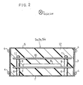
- a case 1 forming part of a housing of each of the sensors Su, Sv and Sw is channel-like.
- An inverted channel-like cover 3 is secured fixedly to the case 1 by screws 4 inserted through both end walls of the cover and the corresponding mounting margins 2 of the case so as to cover both open ends and an upper opening of the case 1.
- a window 5 through which a displacement current flows into the housing (hereinafter referred to as the "displacement current inflow section") is provided in the top of the cover 3.
- the housing including case 1 and cover 3 is made of an electrically conductive material such as aluminum and functions as a shield electrode for a detection electrode 10 to be described in more detail later.
- a base plate 7 fixed to the bottom of the case 1 through supports 6 is a base plate 7 on which is provided a signal processing circuit 8 to be described in more detail later.
- the plate-like collection electrode, into which a displacement current flows, or detection electrode 10 is secured fixedly by means of screws 11 to upper ends of spacers 9 upstanding from the base plate 7.
- the detection electrode 10 is disposed parallel to the upper surface of cover 3 and covered with and isolated from the case 1 and cover 3 except for that portion of electrode 10 opposite to the window 5.
- the detection electrode 10 is made of an electrically conductive material of metal, conductive resin, conductive rubber or the like. In this embodiment, aluminum easy to work is used. After the base plate 7 and detection electrode 10 are assembled, the case 1 is filled up with a filler 12 of high permittivity.
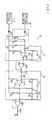
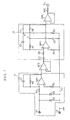
- the signal processing circuit 8 will be described with respect to Figs. 4 and 5. It consists mainly of an amplifier circuit A and a band-pass filter circuit B.
- the amplifier circuit A When the amplifier circuit A receives a displacement current from the detection electrode 10, it amplifies the displacement current and outputs a signal having a wave form similar to that of the displacement current.
- the specific structure of the amplifier circuit is as follows.
- An input terminal P1 of the signal processing circuit 8 is connected via a variable resistor R1 to a grounding conductor E1.
- the case 1 and cover 3 constituting the shield electrode is connected via a terminal P2 to the grounding conductor E1.
- a parallel circuit including a pair of oppositely directed diodes D1 and D2 is connected between both ends of the variable resistor R1 and functions as a protective circuit to shut out an excessive input from the detection electrode 10.
- the resister R1 is connected to an inverting input terminal of an operational amplifier OP1 while an noninverting input terminal of the amplifier is connected via a resistor R3 to the grounding conductor E1.
- a parallel circuit including a capacitor C1 and a resistor R4 is connected between the inverting input terminal and output terminal of the amplifier OP1.
- the resistors R1-R4, diodes D1, D2, capacitor C1 and operational amplifier OP1 constitute the amplifier circuit A, the output terminal of which is connected via a voltage follower including an operational amplifier OP2 to a band-pass filter B of the next stage.
- the follower serves to perform impedance conversion by providing a high input impedance and a low output impedance.
- the band-pass filter B When the band-pass filter B receives a signal having a waveform similar to that of a displacement current from the operational amplifier OP2 constituting the voltage follower, it is arranged to selectively amplify and extract, on the basis of the input signal, a signal having an alternating current waveform, the center frequency of which is 60 Hz.
- the specific circuit of the filter B is as follows. A series circuit including a capacitor 2 and a resistor 5 is connected between the output terminal of the amplifier OP2 and an inverting input terminal of an operational amplifier OP3 which has a noninverting input terminal connected via a resistor R6 to the grounding conductor E1.
- a parallel circuit including a series circuit of capacitors C3, C4 and a series circuit of resistors R7, R8 is connected between the noninverting input terminal and output terminal of operational amplifier OP3.
- a resistor R9 is connected between the grounding conductor E1 and the junction point a of capacitors C3 and C4.
- a capacitor C5 is connected between the grounding conductor E1 and the junction point b of resistors R7 and R8.
- the resistors R5 - R9, capacitors C2 -C5 and amplifier OP3 constitute the band-pass filter B, the output terminal of which is connected via a voltage follower including an operational amplifier OP4 to an output terminal Pu.
- the voltage follower performs impedance conversion by providing a high input impedance and a low output impedance.
- the output terminals of other voltage sensors Sv, Sw are shown by Pv, Pw, respectively, in Fig. 4.
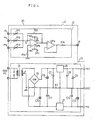
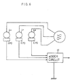
- the voltage sensors Su, Sv and Sw disposed at the corresponding phase distribution lines Lu, Lv and Lw are connected to a zero-phase-sequence sensing unit 20 which includes a sensing circuit 21 which in turn includes an adder circuit 22 and a power supply circuit 23 for the adder circuit and the voltage Sensors.
- the adder circuit 22 synthesizes signals output from the respective voltage sensors Su, Sv and Sw and selected so as to have predetermined frequencies and outputs a zero-phase-sequence voltage signal V0 to its output terminal P.
- the specific structure of adder circuit 22 is as follows.
- the output terminals Pu, Pv, and Pw of the voltage sensors Su, Sv and Sw are connected via the corresponding variable input resistors R11, R12 and R13 to an inverting input terminal G of an operational amplifier OP5 which has a noninvearting input terminal grounded via a resistor 14, and an output terminal connected via a resistor R15 to the point G.
- the output terminal of the amplifier OP5 is connected via a voltage follower including an operational amplifier OP6 and a resistor R16 to the output terminal P.
- the voltage follower OP6 serves to perform impedance conversion by providing a high input impedance and a low output impedance.
- the resistors R11 - R16 and amplifiers OP5 and OP6 constitute the adder circuit 22.
- the power supply circuit 23 Connected to an alternating -current power source 100 V is the primary winding of a current transformer 24 which has the secondary winding connected to a full-wave rectifier 25. A point d of the transformer secondary winding is connected to a grounding line E2. Smoothing capacitor C6 and capacitor C7 are connected between the plus terminal of the rectifier 25 and grounding conductor E2. A 3-terminal regulator 26 is connected between the plus terminal of the rectifier 25 and the grounding conductor E2 and has its output terminal connected to a + Vcc terminal. Capacitors C8 and C9 are connected between the output terminal of the regulator 26 and the grounding conductor E2.
- Smoothing capacitor C10 and capacitor C11 are connected between the minus terminal of the full-wave rectifier 25 and the ground conductor E2.
- a 3-terminal regulator 27 is connected between the minus terminal of full-wave rectifier 25 and the grounding conductor E2 with the output terminal of the regulator 27 being connected to a -Vcc terminal.
- Capacitors 12 and 13 are connected between the output terminal of the regulator 27 and the grounding conductor E2.
- the voltage sensors Su, Sv and Sw are disposed at approximately equal distances l from the corresponding phase distribution lines Lu, Lv and Lw.
- the steady-state load currents on the basis of normal three-phase-sequence voltage flow through the distribution lines, displacement currents flowing through electrostatic capacities Cu, Cv and Cw formed between the respective distribution lines Lu, Lv and Lw and ground as a reference potential collect on the corresponding detection electrodes 10 through the corresponding window 5 in the voltage sensors as the displacement current inflow section (Fig. 2).
- the amplifier circuits A integrate and amplify the corresponding displacement currents and output signals having wave forms similar to those of the displacement currents to the corresponding operational amplifiers OP2.
- the band-pass filters B selectively amplify and extract signals each having an alternating current waveform, the center frequency of which is 60 Hz, on the basis of the corresponding input signals.
- the adder circuit 22 of the zero-phase-sequence sensing unit 20 synthesizes the signals output by the respective voltage sensors Su, Sv and Sw and selected so as to have predetermined frequencies and outputs a zero-phase-sequence voltage signal V0, as shown in Fig. 7, to the output terminal P.
- ⁇ , ⁇ , ⁇ denote the wave forms of voltage applied to the distribution lines Lu, Lv and Lw, respectively.
- the value of the zero-phase-sequence voltage V0 obtained by synthesis at the adder circuit 22 is zero.
- the housing, including case 1 and cover 3, of each of the voltage sensors Su, Sv and Sw functions as a shield electrode which efficiently prevents the inflow of displacement currents from objects other than the distribution line, the voltage on which is to be measured, so that the measurement is hardly influenced adversely by other distribution lines.
- the following measurement was performed in order to compare the output characteristics of the voltage sensors in the zero-phase-sequence voltage sensing apparatus according to this invention with the output characteristics of PDs and voltage sensors X each utilizing a Pockels effect element having a conventional structure.
- the voltage sensors X were directly connected to the corresponding distribution lines Lu, Lv and Lw and the PDs were assembled on the corresponding outer insulation jackets of the lines.
- the voltage sensors according to this invention were each disposed at a distance l of 100 mm under the corresponding distribution line, as in Fig. 1.
- One of the distribution lines was put under a condition similar to grounding.
- the signals output from the voltage sensors X and PDs disposed for the corresponding distribution lines were synthesized by the adder circuit 22 and measured.
- the residual voltage was 65 mV in the use of the conventional voltage sensors X and 4.38 mV in the use of the PDs while the residual voltage was 13.5 mV in the use of the voltage sensors according to the present invention.
- Fig. 7 shows a modification of the signal processing circuit 8, shown in Fig. 3, according to this invention.
- the amplifier circuit A includes no resistor such as the variable resistor R1 shown in Fig. 3 while the output terminal P1 of the detection electrode 10 is connected via a resistor R2 to an inverting input terminal of the operational amplifier OP1.
- This circuit arrangement also operates in a ways similar to that of the above embodiment.
Landscapes
- Physics & Mathematics (AREA)
- General Physics & Mathematics (AREA)
- Measuring Instrument Details And Bridges, And Automatic Balancing Devices (AREA)
- Investigating Or Analyzing Materials By The Use Of Electric Means (AREA)
- Measurement Of Current Or Voltage (AREA)
Applications Claiming Priority (6)
| Application Number | Priority Date | Filing Date | Title |
|---|---|---|---|
| JP246763/85 | 1985-11-01 | ||
| JP24676385 | 1985-11-01 | ||
| JP251496/85 | 1985-11-09 | ||
| JP60251496A JPS62112072A (ja) | 1985-11-09 | 1985-11-09 | 電圧センサ及び同センサを用いた零相電圧検出装置 |
| JP60251495A JPH0668510B2 (ja) | 1985-11-01 | 1985-11-09 | 電圧センサ |
| JP251495/85 | 1985-11-09 |
Related Parent Applications (2)
| Application Number | Title | Priority Date | Filing Date |
|---|---|---|---|
| EP19860115140 Division EP0222278B1 (de) | 1985-11-01 | 1986-10-31 | Spannungsfühler |
| EP86115140.5 Division | 1986-10-31 |
Publications (2)
| Publication Number | Publication Date |
|---|---|
| EP0398396A2 true EP0398396A2 (de) | 1990-11-22 |
| EP0398396A3 EP0398396A3 (de) | 1991-03-20 |
Family
ID=27333517
Family Applications (2)
| Application Number | Title | Priority Date | Filing Date |
|---|---|---|---|
| EP19860115140 Expired - Lifetime EP0222278B1 (de) | 1985-11-01 | 1986-10-31 | Spannungsfühler |
| EP19900113317 Withdrawn EP0398396A3 (de) | 1985-11-01 | 1986-10-31 | Spannungssensor |
Family Applications Before (1)
| Application Number | Title | Priority Date | Filing Date |
|---|---|---|---|
| EP19860115140 Expired - Lifetime EP0222278B1 (de) | 1985-11-01 | 1986-10-31 | Spannungsfühler |
Country Status (3)
| Country | Link |
|---|---|
| US (2) | US4804922A (de) |
| EP (2) | EP0222278B1 (de) |
| DE (1) | DE3678387D1 (de) |
Cited By (2)
| Publication number | Priority date | Publication date | Assignee | Title |
|---|---|---|---|---|
| FR2694408A1 (fr) * | 1992-07-31 | 1994-02-04 | Electricite De France | Dispositif détecteur de défauts sur un réseau de distribution d'énergie électrique aérien. |
| WO2012139650A1 (de) * | 2011-04-14 | 2012-10-18 | Siemens Aktiengesellschaft | Vorrichtung zur berührungslosen bestimmung eines elektrischen potentials eines objekts, stromzange sowie verfahren |
Families Citing this family (30)
| Publication number | Priority date | Publication date | Assignee | Title |
|---|---|---|---|---|
| US5059896A (en) * | 1989-09-25 | 1991-10-22 | General Electric Company | Electronic watthour meter |
| US5296844A (en) * | 1992-01-27 | 1994-03-22 | Ontario Hydro | Electrical contact avoidance device |
| US5350999A (en) * | 1992-03-27 | 1994-09-27 | Brunda Daniel D | Measurement system and method for determining the amount of electromagnetic radiation energy being absorbed by living beings |
| US5270660A (en) * | 1992-05-05 | 1993-12-14 | Xerox Corporation | Electrostatic voltmeter employing high voltage integrated circuit devices |
| US5357393A (en) * | 1992-05-05 | 1994-10-18 | Xerox Corporation | Integrated ultra low leakage high voltage protection circuit |
| US5323115A (en) * | 1992-05-05 | 1994-06-21 | Xerox Corporation | Electrostatic voltmeter producing a low voltage output |
| FI93998C (fi) * | 1992-06-22 | 1995-06-26 | Sekko Ab Oy | Menetelmä ja laite kiertosuunnan mittaamiseen |
| US5315255A (en) * | 1992-07-16 | 1994-05-24 | Micron Technology, Inc. | Non-contact, electrostatic, discharge detector |
| US5406437A (en) * | 1994-04-14 | 1995-04-11 | Levin; Michael I. | Zero phase sequence current filter with adjustable impedance |
| US5633700A (en) * | 1994-10-31 | 1997-05-27 | Xerox Corporation | Actuator for actuating a surface contacting probe of a contacting electrostatic voltmeter |
| US5488301A (en) * | 1994-12-19 | 1996-01-30 | Xerox Corporation | Electrostatic voltmeter employing a differential cascode |
| US5952820A (en) * | 1996-02-16 | 1999-09-14 | Thrasher; M. D. | Foreign voltage detector |
| US5910775A (en) * | 1996-08-29 | 1999-06-08 | S&C Electric Company | Phasing and indicator arrangements for switchgear or the like |
| US6411108B1 (en) | 1999-11-05 | 2002-06-25 | Sensor Technologies, Inc. | Noncontact signal analyzer |
| SE519259C2 (sv) * | 2000-02-25 | 2003-02-04 | Vattenfall Ab | Sätt och system för övervakning av en elfördelningscentral,samt användning av systemet |
| US6426630B1 (en) * | 2000-11-29 | 2002-07-30 | Xerox Corporation | Electrostatic voltmeter with current source load |
| US6545483B1 (en) | 2001-08-29 | 2003-04-08 | Sensor Technologies, Inc. | Analyzer sensor |
| US6828767B2 (en) | 2002-03-20 | 2004-12-07 | Santronics, Inc. | Hand-held voltage detection probe |
| JP4511136B2 (ja) | 2003-07-25 | 2010-07-28 | 日本高圧電気株式会社 | 非接触式センサ |
| EP1761789A1 (de) * | 2004-07-01 | 2007-03-14 | Quantum Applied Science and Research, Inc. | Sensorsystem zur messung elektrischer potenzialsignale von objekten |
| US7511909B2 (en) * | 2004-09-20 | 2009-03-31 | Agency For Science, Technology And Research | Sector based timing recovery for a readback signal |
| US20060192545A1 (en) * | 2005-02-28 | 2006-08-31 | Static Control Components, Inc. | Voltage detection pole |
| US8193802B2 (en) * | 2008-04-09 | 2012-06-05 | Milwaukee Electric Tool Corporation | Slidably attachable non-contact voltage detector |
| TWI439700B (zh) | 2012-01-19 | 2014-06-01 | 財團法人工業技術研究院 | 用於具有雙導線之電力電纜線的電力感測裝置 |
| ES2667483T3 (es) * | 2014-11-04 | 2018-05-11 | Abb Schweiz Ag | Una unidad de fuente de alimentación para un dispositivo electrónico inteligente auto-alimentado |
| US10132842B2 (en) * | 2015-04-01 | 2018-11-20 | Eaton Intelligent Power Limited | Virtual ground sensing circuit for high impedance voltage sensors |
| USD769139S1 (en) | 2015-12-10 | 2016-10-18 | Power Solutions, Inc. | Probe |
| DE102015121876A1 (de) | 2015-12-15 | 2017-06-22 | Bombardier Transportation Gmbh | Vorrichtung zum Erkennen eines Spannungssystems |
| DE102015121879A1 (de) * | 2015-12-15 | 2017-06-22 | Bombardier Transportation Gmbh | Verfahren zum Steuern einer Kontaktkraft zwischen einem Fahrdraht und mindestens einem Stromabnehmer eines Schienenfahrzeugs |
| US10466280B1 (en) | 2018-04-13 | 2019-11-05 | Power Solutions, Inc. | Enhanced circuit and method for detecting hazardous foreign voltages on conductors |
Family Cites Families (26)
| Publication number | Priority date | Publication date | Assignee | Title |
|---|---|---|---|---|
| US1504614A (en) * | 1921-09-01 | 1924-08-12 | Westinghouse Electric & Mfg Co | Electric measuring instrument |
| USRE21151E (en) * | 1931-09-08 | 1939-07-18 | Radio receiving system | |
| US2137579A (en) * | 1935-04-01 | 1938-11-22 | Ericsson Telefon Ab L M | Alternating current power circuit |
| US2468125A (en) * | 1943-07-14 | 1949-04-26 | Walter T Silver | Standing wave indicator |
| US2756414A (en) * | 1952-03-01 | 1956-07-24 | Motorola Inc | Coupling unit |
| DE1132653B (de) * | 1959-12-18 | 1962-07-05 | Peter Sidney Vick | Elektrodensystem zum beruehrungslosen, kapazitiven Pruefen elektrischer, stromfuehrender Leiter |
| DE1134157B (de) * | 1959-12-22 | 1962-08-02 | John Lunn Douglas | Vorrichtung zum Feststellen des Spannungsfuehrens von unter Wechselspannung setzbaren elektrischen Leitern |
| CH436475A (de) * | 1964-09-30 | 1967-05-31 | Promotechnic Ag | Vorrichtung zum Nachweis von elektrischen Spannungen |
| US3383565A (en) * | 1966-05-13 | 1968-05-14 | Gen Electric | Packaging of electrical components |
| US3524133A (en) * | 1966-09-09 | 1970-08-11 | Gen Electric | Static state voltage and current monitoring device for electric power cable terminations |
| US3774108A (en) * | 1971-12-13 | 1973-11-20 | Frl Inc | Electrostatic potential detector |
| FR2206507B1 (de) * | 1972-11-10 | 1976-04-23 | Electricite De France | |
| US3825768A (en) * | 1973-02-15 | 1974-07-23 | Eaton Corp | Phase sequence and power loss detector |
| US4121154A (en) * | 1975-10-14 | 1978-10-17 | The United States Of America As Represented By The Secretary Of The Interior | Alternating current potential measuring device |
| US4146913A (en) * | 1977-12-30 | 1979-03-27 | Westinghouse Electric Corp. | Symmetrical component sequence filter |
| US4197493A (en) * | 1978-05-11 | 1980-04-08 | Hewlett-Packard Company | Electrostatic voltmeter |
| GB2035728B (en) * | 1978-11-30 | 1982-10-13 | Plessey Co Ltd | Openphase detector |
| JPS55114962A (en) * | 1979-02-28 | 1980-09-04 | Ricoh Co Ltd | Surface potentiometer |
| DE3119925C2 (de) * | 1981-07-10 | 1983-07-21 | András Dipl.-Ing. 1116 Budapest Bely | Verfahren und Gerät zur Erdschlußortung an Starkstrom-Freileitungsnetzen |
| US4504781A (en) * | 1982-09-30 | 1985-03-12 | Hargrove Douglas L | Voltage wand |
| US4427945A (en) * | 1982-10-28 | 1984-01-24 | Beckman Instruments, Inc. | Molded conductivity cell body |
| US4520318A (en) * | 1983-02-17 | 1985-05-28 | Marcel Hascal | Electric field strength indicator |
| US4479160A (en) * | 1983-05-02 | 1984-10-23 | Westinghouse Electric Corp. | Band-pass sequence filters for symmetrical components of multiphase AC power systems |
| JPS6122463A (ja) * | 1984-07-09 | 1986-01-31 | Matsushita Electric Ind Co Ltd | 磁気記録再生装置 |
| JPS6122465A (ja) * | 1984-07-10 | 1986-01-31 | Matsushita Electric Ind Co Ltd | カセツト移送装置 |
| JPS6122466A (ja) * | 1984-07-10 | 1986-01-31 | Matsushita Electric Ind Co Ltd | カセツト移送装置 |
-
1986
- 1986-10-27 US US06/923,560 patent/US4804922A/en not_active Expired - Fee Related
- 1986-10-31 DE DE8686115140T patent/DE3678387D1/de not_active Expired - Fee Related
- 1986-10-31 EP EP19860115140 patent/EP0222278B1/de not_active Expired - Lifetime
- 1986-10-31 EP EP19900113317 patent/EP0398396A3/de not_active Withdrawn
-
1988
- 1988-10-24 US US07/261,441 patent/US4879509A/en not_active Expired - Fee Related
Cited By (7)
| Publication number | Priority date | Publication date | Assignee | Title |
|---|---|---|---|---|
| FR2694408A1 (fr) * | 1992-07-31 | 1994-02-04 | Electricite De France | Dispositif détecteur de défauts sur un réseau de distribution d'énergie électrique aérien. |
| WO1994003953A1 (fr) * | 1992-07-31 | 1994-02-17 | Electricite De France - Service National | Dispositif detecteur de defauts sur un reseau de distribution d'energie electrique aerien |
| EP0586273A1 (de) * | 1992-07-31 | 1994-03-09 | Electricite De France | Detektionsvorrichtung für Fehler auf einem Freileitungsnetz für elektrische Energieverteilung |
| WO2012139650A1 (de) * | 2011-04-14 | 2012-10-18 | Siemens Aktiengesellschaft | Vorrichtung zur berührungslosen bestimmung eines elektrischen potentials eines objekts, stromzange sowie verfahren |
| CN103582821A (zh) * | 2011-04-14 | 2014-02-12 | 西门子公司 | 用于无接触确定对象的电位的装置、测电钳以及方法 |
| CN103582821B (zh) * | 2011-04-14 | 2015-11-25 | 西门子公司 | 用于无接触确定对象的电位的装置、测电钳以及方法 |
| US9664720B2 (en) | 2011-04-14 | 2017-05-30 | Siemens Aktiengesellschaft | Device for the contactless determination of an electrical potential of an object, current probe, and method |
Also Published As
| Publication number | Publication date |
|---|---|
| DE3678387D1 (de) | 1991-05-02 |
| EP0398396A3 (de) | 1991-03-20 |
| US4879509A (en) | 1989-11-07 |
| EP0222278A1 (de) | 1987-05-20 |
| EP0222278B1 (de) | 1991-03-27 |
| US4804922A (en) | 1989-02-14 |
Similar Documents
| Publication | Publication Date | Title |
|---|---|---|
| EP0398396A2 (de) | Spannungssensor | |
| US4240059A (en) | Current divider for a current sensing transducer | |
| AU701621B2 (en) | A device for sensing of electric discharges in a test object | |
| US4616176A (en) | Dynamic current transducer | |
| US5386193A (en) | Partial discharge detecting device for resin-molded transformer | |
| RU2115131C1 (ru) | Устройство для определения тангенса угла диэлектрических потерь | |
| JPH0668510B2 (ja) | 電圧センサ | |
| JPH0579147B2 (de) | ||
| JPS62112072A (ja) | 電圧センサ及び同センサを用いた零相電圧検出装置 | |
| SU1480008A1 (ru) | Устройство дл измерени емкости сети под рабочим напр жением | |
| JPH0792481B2 (ja) | ガス絶縁密閉電器の電圧および部分放電検出装置 | |
| SU1138762A1 (ru) | Устройство дл измерени электрической проводимости | |
| JPH0862264A (ja) | 電力ケーブルの絶縁抵抗測定装置 | |
| JPH0668507B2 (ja) | 電圧センサ付き開閉器 | |
| SU1725134A1 (ru) | Устройство дл измерени электрической энергии | |
| RU2099725C1 (ru) | Способ измерения тангенса угла потерь высоковольтного оборудования и устройство для его осуществления | |
| SU1591131A2 (ru) | Устройство для защиты от внутренних повреждений шунтовой конденсаторной батареи, собранной в треугольник | |
| SU1095099A1 (ru) | Устройство дл измерени электрической проводимости | |
| SU430337A1 (ru) | Установка для испытаний мощных высоковольтных шунтирующих реакторов | |
| SU1751700A1 (ru) | Устройство дл определени рассто ни до места повреждени изол ции жил кабел | |
| SU1215032A1 (ru) | Устройство дл измерени электрической проводимости жидкости | |
| SU1432422A1 (ru) | Устройство дл измерени активного сопротивлени изол ции в сет х с заземленной нейтралью | |
| SU612332A1 (ru) | Устройство дл защиты отзамыкани на корпус электроустановки в сети переменного тока | |
| SU962820A1 (ru) | Устройство дл измерени емкости в заводских высоковольтных распределительных сет х под рабочим напр жением | |
| SU1746331A1 (ru) | Способ контрол сопротивлени междуфазной изол ции обмоток трехфазной электрической машины и устройство дл его осуществлени |
Legal Events
| Date | Code | Title | Description |
|---|---|---|---|
| PUAI | Public reference made under article 153(3) epc to a published international application that has entered the european phase |
Free format text: ORIGINAL CODE: 0009012 |
|
| AC | Divisional application: reference to earlier application |
Ref document number: 222278 Country of ref document: EP |
|
| AK | Designated contracting states |
Kind code of ref document: A2 Designated state(s): DE FR GB |
|
| PUAL | Search report despatched |
Free format text: ORIGINAL CODE: 0009013 |
|
| AK | Designated contracting states |
Kind code of ref document: A3 Designated state(s): DE FR GB |
|
| RHK1 | Main classification (correction) |
Ipc: G01R 29/16 |
|
| 17P | Request for examination filed |
Effective date: 19910826 |
|
| 17Q | First examination report despatched |
Effective date: 19930126 |
|
| STAA | Information on the status of an ep patent application or granted ep patent |
Free format text: STATUS: THE APPLICATION IS DEEMED TO BE WITHDRAWN |
|
| 18D | Application deemed to be withdrawn |
Effective date: 19930608 |