EP0398801A1 - Detektoreinheit für Infrarotüberwachungssystem - Google Patents
Detektoreinheit für Infrarotüberwachungssystem Download PDFInfo
- Publication number
- EP0398801A1 EP0398801A1 EP90401299A EP90401299A EP0398801A1 EP 0398801 A1 EP0398801 A1 EP 0398801A1 EP 90401299 A EP90401299 A EP 90401299A EP 90401299 A EP90401299 A EP 90401299A EP 0398801 A1 EP0398801 A1 EP 0398801A1
- Authority
- EP
- European Patent Office
- Prior art keywords
- detectors
- standby
- imaging
- samples
- grouping
- Prior art date
- Legal status (The legal status is an assumption and is not a legal conclusion. Google has not performed a legal analysis and makes no representation as to the accuracy of the status listed.)
- Granted
Links
Images

Classifications
-
- H—ELECTRICITY
- H04—ELECTRIC COMMUNICATION TECHNIQUE
- H04N—PICTORIAL COMMUNICATION, e.g. TELEVISION
- H04N25/00—Circuitry of solid-state image sensors [SSIS]; Control thereof
- H04N25/70—SSIS architectures; Circuits associated therewith
- H04N25/71—Charge-coupled device [CCD] sensors; Charge-transfer registers specially adapted for CCD sensors
- H04N25/711—Time delay and integration [TDI] registers; TDI shift registers
-
- H—ELECTRICITY
- H04—ELECTRIC COMMUNICATION TECHNIQUE
- H04N—PICTORIAL COMMUNICATION, e.g. TELEVISION
- H04N23/00—Cameras or camera modules comprising electronic image sensors; Control thereof
- H04N23/20—Cameras or camera modules comprising electronic image sensors; Control thereof for generating image signals from infrared radiation only
Definitions
- the present invention relates to a detection assembly for infrared, panoramic or sectoral standby system.
- Such a detection assembly may include an optical device, in the focal plane thereof, a strip of detectors - infrared photodiodes - for analyzing landscapes, or backdrops, hybridized to a pretreatment plate containing circuits charge transfer, namely, and essentially, input circuits associated with photodiodes, to integrate their output currents, preamplification, filtering and multiplexing circuits and an output circuit forming an interface between the preprocessing board and a separate subsequent treatment strip.
- a pretreatment plate containing circuits charge transfer, namely, and essentially, input circuits associated with photodiodes, to integrate their output currents, preamplification, filtering and multiplexing circuits and an output circuit forming an interface between the preprocessing board and a separate subsequent treatment strip.
- the output current of each photodiode can therefore be processed in an integration circuit delivering a charge signal to a delay line in which it undergoes a determined phase shift, the charge signals delivered by all the delay lines associated with the photodiodes of the same line being added in an adder.
- the circuit in question is a delay-summation circuit called TDI (time delay integration).
- the pre-treatment plate can also include trimming, evacuation and anti-glare circuits, this latter function aiming to divert all the diode current when it is too high and to prevent a saturated current from damaging the operation of the circuits of the treatment board.
- infrared detection systems are used either in standby systems, in imaging systems, or in combined systems.
- the elementary detectors of the analysis strip must be as small as possible to obtain the best possible angular resolution and thus optimize the performance of recognition range and 'identification.
- the elementary detectors of the bars used until now were on the contrary large enough to adapt to the optical spots produced by the hot spots of the objects (planes and other targets) to be detected and whose temperature is much higher to that of the background.
- the present invention therefore aims to overcome these drawbacks.
- the present invention relates to a detection assembly for an infrared standby system intended for the detection of hot objects on a backdrop, comprising a strip of elementary infrared detectors for analyzing the backdrop, detection assembly characterized by the fact that the elementary detectors are imaging detectors of sensitive surfaces smaller than the optical spots produced by hot objects to be detected and it includes means arranged to virtually group the imaging detectors into virtual detectors for monitoring sensitive surfaces adapted to said optical spots.
- geometry correction means are provided for, before grouping them into virtual standby detectors, grouping the elementary imaging detectors into m intermediate virtual detectors contiguous and aligned in a column, with the same sensitive surface as the imaging detectors.
- the grouping means can be bidirectional grouping, in deposit and in site.
- These grouping means may include means for summing, in the direction of the sites, p intermediate detectors contiguous to the step of q, less than p, detectors, with, therefore, an overlap of (pq) intermediate detectors from one standby detector to the next.
- the means for grouping the assembly of the invention can advantageously include means for summing in deposit similar to the means for summing in site, with an overlap of (rs) intermediate samples of a detector, or pixel, of standby next.
- the ratio between the number of standby pixels and the number of imaging pixels is 1 qs .
- This bidirectional summation provides a significant gain: - the signal attenuations of the point targets located at the spatial limit between two lines scanned by two contiguous detectors in the direction perpendicular to that of the scan; the probability of detection is therefore increased; - we improve the report by adapting the geometry to the dimensions of the optical spots; - the signal processing rate is reduced, in the case mentioned by qs, and it is thus possible, taking into account the technologies available, to implement efficient target extraction algorithms.
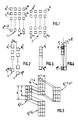
- Mosaic 1 thus comprises a first line of four detectors d i 11 ... d i 14, a second line of detectors d i 31 ... d i 34 ... and a last row of detectors d i m-1, 1 ... d i m-1,4 and mosaic 2, a first line of detectors d i 21 ... d i 24 ... and a last line of detectors d i m1 ... d i m4 , the lines of the two mosaics being alternated and without overlap.
- a first grouping is carried out by TDI summation to group the four imaging detectors of each line of each mosaic and obtain two columns 3, 4 of intermediate virtual detectors d l 1 ... d l m-1 and d l 2 ... d l m , respectively alternated from one column to the other and without overlap, the two columns being offset in time by deposit of k samples e in the sense always described from the preamble ( Figure 2).
- a second geometry correction is carried out to group the detectors of the two columns 3, 4 into a single column 5 of m detectors d l 1 ... d l m aligned in elevation , contiguous and of sensitive surface substantially equal to that of the detectors d imagery of i (figure 3).
- a sample e l has the same dimension in site as an intermediate detector d l and a useful dimension in smaller field due to an overlap due to the sliding in field of the bar 5 during its reading in site.
- the detectors d v are constituted by summation in site of p samples e l at the step of q and by summation at the site of r samples e l at the step of s.
- the virtual bar 5, extending in the direction of the sites, is displaced - it is naturally a relative displacement - perpendicular to itself in the direction of the deposits.
- standby detectors we are actually referring to; in the direction of the deposits, to image elements or pixels.
- the values of the parameters p, q, r, s and k are programmable and the detectors or standby pixels are obtained using a calculation automaton produced here by a specific ASIC circuit integrated on a standard card.
- the standby cells d v ij thus obtained are adapted in bearing to the optical spot and they are elongated in elevation, the overlapping of the contiguous cells having to allow not to lose in detection level if an optical spot covers two cells.
- each watch cell d v ij can also cover the two cells d v il, j and d v i + l, j to which it is contiguous.
- FIG. 6 shows a portion 1 of the specific integrated circuit for generating standby cells or pixels from imaging pixels, which includes a block 2 of even cells and a block 3 of all cells.
- the imaging pixels d i of even ranks, those on the right in FIG. 1, which enter at 4 in block 2, are grouped therein by a multiplexer 5 followed by an adder 6, the output of which is connected to one of the inputs of the multiplexer 5 by a buffer memory 7.
- the pixels exiting from block 2 at 8, those on the right in FIG. 2, enter a time-catching memory 9 the output of which is connected to the input of the block 3 and, more precisely at an input of a multiplexer 10 of which another input receives the imaging pixels d i of odd rows, those on the left in FIG. 1.
- the output of the multiplexer 10 of block 3 is connected to the input of an adder 11, the output of which is connected to a third input of the multiplexer 10 by a training RAM 12 of watch cells.
- Blocks 2 and 3 are connected to a sequencer 13 controlled by a ROM memory 14 containing the parameters p, q, r, s, k.
- the imaging pixels of even ranks are shifted into a deposit of k samples, after temporal catching up of the fourth imaging pixels of odd ranks: this is the second geometry correction mentioned above in reference to figure 3.
- All the imaging samples are added up on site and in deposit in block 3, the sum of the samples passing through a dividing block 15, comprising in this case a PROM memory, connected to the output of block 3 and controlled by the sequencer. 13, to be divided, in site and in deposit, and to provide the standby cells of FIG. 5.
- a dividing block 15 comprising in this case a PROM memory, connected to the output of block 3 and controlled by the sequencer. 13, to be divided, in site and in deposit, and to provide the standby cells of FIG. 5.
- the specific integrated circuit here comprises three other portions identical to the portion 1 described above, connected in parallel to the divider 15.
Landscapes
- Engineering & Computer Science (AREA)
- Multimedia (AREA)
- Signal Processing (AREA)
- Photometry And Measurement Of Optical Pulse Characteristics (AREA)
- Transforming Light Signals Into Electric Signals (AREA)
- Radiation Pyrometers (AREA)
Applications Claiming Priority (2)
| Application Number | Priority Date | Filing Date | Title |
|---|---|---|---|
| FR8906482 | 1989-05-18 | ||
| FR8906482A FR2647203B1 (fr) | 1989-05-18 | 1989-05-18 | Ensemble de detection pour systeme de veille infrarouge |
Publications (2)
| Publication Number | Publication Date |
|---|---|
| EP0398801A1 true EP0398801A1 (de) | 1990-11-22 |
| EP0398801B1 EP0398801B1 (de) | 1994-09-21 |
Family
ID=9381753
Family Applications (1)
| Application Number | Title | Priority Date | Filing Date |
|---|---|---|---|
| EP90401299A Expired - Lifetime EP0398801B1 (de) | 1989-05-18 | 1990-05-16 | Detektoreinheit für Infrarotüberwachungssystem |
Country Status (4)
| Country | Link |
|---|---|
| EP (1) | EP0398801B1 (de) |
| CA (1) | CA2017042C (de) |
| DE (1) | DE69012649T2 (de) |
| FR (1) | FR2647203B1 (de) |
Cited By (1)
| Publication number | Priority date | Publication date | Assignee | Title |
|---|---|---|---|---|
| EP0895411A3 (de) * | 1997-08-02 | 1999-02-17 | Gec-Marconi Limited | Abbildungssystem |
Citations (4)
| Publication number | Priority date | Publication date | Assignee | Title |
|---|---|---|---|---|
| EP0023131A1 (de) * | 1979-07-20 | 1981-01-28 | The Rank Organisation Limited | Optische Abtastvorrichtungen |
| EP0224228A2 (de) * | 1985-11-26 | 1987-06-03 | Honeywell Inc. | Verfahren und Einrichtung zur Verarbeitung von rasterabgetasteten Bildsignalen |
| EP0230809A1 (de) * | 1985-12-10 | 1987-08-05 | SAT Société Anonyme de Télécommunications | Wärmebildkamera mit Parallelabtastung |
| GB2191059A (en) * | 1985-08-02 | 1987-12-02 | Trt Telecom Radio Electr | Electronic interlaced scanning, for a thermal camera |
-
1989
- 1989-05-18 FR FR8906482A patent/FR2647203B1/fr not_active Expired - Fee Related
-
1990
- 1990-05-16 EP EP90401299A patent/EP0398801B1/de not_active Expired - Lifetime
- 1990-05-16 DE DE69012649T patent/DE69012649T2/de not_active Expired - Fee Related
- 1990-05-17 CA CA002017042A patent/CA2017042C/fr not_active Expired - Fee Related
Patent Citations (4)
| Publication number | Priority date | Publication date | Assignee | Title |
|---|---|---|---|---|
| EP0023131A1 (de) * | 1979-07-20 | 1981-01-28 | The Rank Organisation Limited | Optische Abtastvorrichtungen |
| GB2191059A (en) * | 1985-08-02 | 1987-12-02 | Trt Telecom Radio Electr | Electronic interlaced scanning, for a thermal camera |
| EP0224228A2 (de) * | 1985-11-26 | 1987-06-03 | Honeywell Inc. | Verfahren und Einrichtung zur Verarbeitung von rasterabgetasteten Bildsignalen |
| EP0230809A1 (de) * | 1985-12-10 | 1987-08-05 | SAT Société Anonyme de Télécommunications | Wärmebildkamera mit Parallelabtastung |
Cited By (2)
| Publication number | Priority date | Publication date | Assignee | Title |
|---|---|---|---|---|
| EP0895411A3 (de) * | 1997-08-02 | 1999-02-17 | Gec-Marconi Limited | Abbildungssystem |
| US5986810A (en) * | 1997-08-02 | 1999-11-16 | Gec-Marconi Limited | Imaging system |
Also Published As
| Publication number | Publication date |
|---|---|
| FR2647203B1 (fr) | 1995-09-08 |
| CA2017042A1 (fr) | 1990-11-18 |
| FR2647203A1 (fr) | 1990-11-23 |
| DE69012649D1 (de) | 1994-10-27 |
| DE69012649T2 (de) | 1995-04-13 |
| EP0398801B1 (de) | 1994-09-21 |
| CA2017042C (fr) | 2000-09-19 |
Similar Documents
| Publication | Publication Date | Title |
|---|---|---|
| FR2736492A1 (fr) | Procede et systeme pour compenser le deplacement pendant la formation d'image | |
| EP0920677B1 (de) | Verfahren und vorrichtung zur lufterde erkennung für eine elektronische anlage | |
| FR2503391A1 (fr) | Systeme de balayage optique | |
| EP0254634A1 (de) | Verfahren und Vorrichtung zum optischen Abstandsmessen | |
| EP0435768B1 (de) | Verfahren und Anordnung zur Lagebestimmung eines bewegten Körpers durch Verfolgen einer auf dem Körper angeordneten Markierung | |
| EP3423860B1 (de) | Vorrichtung zur erkennung eines laserflecks | |
| FR2672989A1 (fr) | Dispositif de determination de la direction d'une source emissive de faible luminosite et son application a la visee stellaire. | |
| FR2682186A1 (fr) | Detecteur infrarouge a haute sensibilite et camera infrarouge utilisant un tel detecteur. | |
| EP3777129B1 (de) | Luftbildsensor zur aufnahme von matrixbildern durch zeitliche verschiebung und multispektrale summation | |
| EP0398801B1 (de) | Detektoreinheit für Infrarotüberwachungssystem | |
| EP0425348B1 (de) | Programmierbare Integrationszeit für Photosensor | |
| EP0604302B1 (de) | Verfahren und Vorrichtung zur Analyse von sich bewegenden Objekten mittels Radiographie | |
| FR2944363A1 (fr) | Procede et systeme d'imagerie active a champ large | |
| CA1266523A (fr) | Senseur opto-electronique multichamp a transfert de charges | |
| EP1535463B1 (de) | Verfahren und sensor zur bestimmung des lokalen kontrastes einer beobachteten szene durch detektion der von dieser szene abgestrahlten luminanz | |
| EP0352309A1 (de) | Anordnung und vorrichtung zur erzeugung und verarbeitung von abgetasteten netzmustern. | |
| CA1263170A (fr) | Senseur opto-electronique a transfert de charges | |
| WO2011138542A1 (fr) | Procede d'imagerie | |
| US5229609A (en) | Detection assembly for an infrared monitoring system | |
| EP3839814B1 (de) | Bordseitiges optisches beobachtungsinstrument mit variabler räumlicher und spektraler auflösung | |
| FR2677207A1 (fr) | Dispositif de prise de vues opto-electronique a defilement. | |
| FR2551201A1 (fr) | Dispositif pour determiner les variations d'orientation d'un engin spatial | |
| EP3797510B1 (de) | Panoramabeobachtungssystem für plattform | |
| EP1329846A1 (de) | Anordnung zur Detektion punktförmiger Ziele durch räumliche und zeitliche Bildverarbeitung | |
| CA3231635A1 (fr) | Procede pour l'acquisition d'images multispectrales et d'imagettes panchromatiques |
Legal Events
| Date | Code | Title | Description |
|---|---|---|---|
| PUAI | Public reference made under article 153(3) epc to a published international application that has entered the european phase |
Free format text: ORIGINAL CODE: 0009012 |
|
| AK | Designated contracting states |
Kind code of ref document: A1 Designated state(s): DE GB IT |
|
| 17P | Request for examination filed |
Effective date: 19901224 |
|
| 17Q | First examination report despatched |
Effective date: 19930414 |
|
| GRAA | (expected) grant |
Free format text: ORIGINAL CODE: 0009210 |
|
| AK | Designated contracting states |
Kind code of ref document: B1 Designated state(s): DE GB IT |
|
| REF | Corresponds to: |
Ref document number: 69012649 Country of ref document: DE Date of ref document: 19941027 |
|
| GBT | Gb: translation of ep patent filed (gb section 77(6)(a)/1977) |
Effective date: 19941020 |
|
| ITF | It: translation for a ep patent filed | ||
| PLBE | No opposition filed within time limit |
Free format text: ORIGINAL CODE: 0009261 |
|
| STAA | Information on the status of an ep patent application or granted ep patent |
Free format text: STATUS: NO OPPOSITION FILED WITHIN TIME LIMIT |
|
| 26N | No opposition filed | ||
| REG | Reference to a national code |
Ref country code: GB Ref legal event code: IF02 |
|
| PGFP | Annual fee paid to national office [announced via postgrant information from national office to epo] |
Ref country code: GB Payment date: 20060502 Year of fee payment: 17 |
|
| PGFP | Annual fee paid to national office [announced via postgrant information from national office to epo] |
Ref country code: DE Payment date: 20060510 Year of fee payment: 17 |
|
| PGFP | Annual fee paid to national office [announced via postgrant information from national office to epo] |
Ref country code: IT Payment date: 20060531 Year of fee payment: 17 |
|
| GBPC | Gb: european patent ceased through non-payment of renewal fee |
Effective date: 20070516 |
|
| PG25 | Lapsed in a contracting state [announced via postgrant information from national office to epo] |
Ref country code: DE Free format text: LAPSE BECAUSE OF NON-PAYMENT OF DUE FEES Effective date: 20071201 |
|
| PG25 | Lapsed in a contracting state [announced via postgrant information from national office to epo] |
Ref country code: GB Free format text: LAPSE BECAUSE OF NON-PAYMENT OF DUE FEES Effective date: 20070516 |
|
| PG25 | Lapsed in a contracting state [announced via postgrant information from national office to epo] |
Ref country code: IT Free format text: LAPSE BECAUSE OF NON-PAYMENT OF DUE FEES Effective date: 20070516 |