EP0399265A2 - Substrat, verwendbar bei der Herstellung einer Dickschichtschaltung - Google Patents
Substrat, verwendbar bei der Herstellung einer Dickschichtschaltung Download PDFInfo
- Publication number
- EP0399265A2 EP0399265A2 EP90108447A EP90108447A EP0399265A2 EP 0399265 A2 EP0399265 A2 EP 0399265A2 EP 90108447 A EP90108447 A EP 90108447A EP 90108447 A EP90108447 A EP 90108447A EP 0399265 A2 EP0399265 A2 EP 0399265A2
- Authority
- EP
- European Patent Office
- Prior art keywords
- surface film
- oxide
- residual
- film
- foundation
- Prior art date
- Legal status (The legal status is an assumption and is not a legal conclusion. Google has not performed a legal analysis and makes no representation as to the accuracy of the status listed.)
- Granted
Links
Images

Classifications
-
- H—ELECTRICITY
- H10—SEMICONDUCTOR DEVICES; ELECTRIC SOLID-STATE DEVICES NOT OTHERWISE PROVIDED FOR
- H10W—GENERIC PACKAGES, INTERCONNECTIONS, CONNECTORS OR OTHER CONSTRUCTIONAL DETAILS OF DEVICES COVERED BY CLASS H10
- H10W70/00—Package substrates; Interposers; Redistribution layers [RDL]
- H10W70/60—Insulating or insulated package substrates; Interposers; Redistribution layers
- H10W70/67—Insulating or insulated package substrates; Interposers; Redistribution layers characterised by their insulating layers or insulating parts
- H10W70/69—Insulating materials thereof
- H10W70/692—Ceramics or glasses
-
- H—ELECTRICITY
- H05—ELECTRIC TECHNIQUES NOT OTHERWISE PROVIDED FOR
- H05K—PRINTED CIRCUITS; CASINGS OR CONSTRUCTIONAL DETAILS OF ELECTRIC APPARATUS; MANUFACTURE OF ASSEMBLAGES OF ELECTRICAL COMPONENTS
- H05K3/00—Apparatus or processes for manufacturing printed circuits
- H05K3/38—Improvement of the adhesion between the insulating substrate and the metal
-
- H—ELECTRICITY
- H10—SEMICONDUCTOR DEVICES; ELECTRIC SOLID-STATE DEVICES NOT OTHERWISE PROVIDED FOR
- H10W—GENERIC PACKAGES, INTERCONNECTIONS, CONNECTORS OR OTHER CONSTRUCTIONAL DETAILS OF DEVICES COVERED BY CLASS H10
- H10W90/00—Package configurations
-
- H—ELECTRICITY
- H10—SEMICONDUCTOR DEVICES; ELECTRIC SOLID-STATE DEVICES NOT OTHERWISE PROVIDED FOR
- H10W—GENERIC PACKAGES, INTERCONNECTIONS, CONNECTORS OR OTHER CONSTRUCTIONAL DETAILS OF DEVICES COVERED BY CLASS H10
- H10W74/00—Encapsulations, e.g. protective coatings
-
- Y—GENERAL TAGGING OF NEW TECHNOLOGICAL DEVELOPMENTS; GENERAL TAGGING OF CROSS-SECTIONAL TECHNOLOGIES SPANNING OVER SEVERAL SECTIONS OF THE IPC; TECHNICAL SUBJECTS COVERED BY FORMER USPC CROSS-REFERENCE ART COLLECTIONS [XRACs] AND DIGESTS
- Y10—TECHNICAL SUBJECTS COVERED BY FORMER USPC
- Y10S—TECHNICAL SUBJECTS COVERED BY FORMER USPC CROSS-REFERENCE ART COLLECTIONS [XRACs] AND DIGESTS
- Y10S428/00—Stock material or miscellaneous articles
- Y10S428/901—Printed circuit
-
- Y—GENERAL TAGGING OF NEW TECHNOLOGICAL DEVELOPMENTS; GENERAL TAGGING OF CROSS-SECTIONAL TECHNOLOGIES SPANNING OVER SEVERAL SECTIONS OF THE IPC; TECHNICAL SUBJECTS COVERED BY FORMER USPC CROSS-REFERENCE ART COLLECTIONS [XRACs] AND DIGESTS
- Y10—TECHNICAL SUBJECTS COVERED BY FORMER USPC
- Y10T—TECHNICAL SUBJECTS COVERED BY FORMER US CLASSIFICATION
- Y10T428/00—Stock material or miscellaneous articles
- Y10T428/24—Structurally defined web or sheet [e.g., overall dimension, etc.]
- Y10T428/24802—Discontinuous or differential coating, impregnation or bond [e.g., artwork, printing, retouched photograph, etc.]
- Y10T428/24917—Discontinuous or differential coating, impregnation or bond [e.g., artwork, printing, retouched photograph, etc.] including metal layer
-
- Y—GENERAL TAGGING OF NEW TECHNOLOGICAL DEVELOPMENTS; GENERAL TAGGING OF CROSS-SECTIONAL TECHNOLOGIES SPANNING OVER SEVERAL SECTIONS OF THE IPC; TECHNICAL SUBJECTS COVERED BY FORMER USPC CROSS-REFERENCE ART COLLECTIONS [XRACs] AND DIGESTS
- Y10—TECHNICAL SUBJECTS COVERED BY FORMER USPC
- Y10T—TECHNICAL SUBJECTS COVERED BY FORMER US CLASSIFICATION
- Y10T428/00—Stock material or miscellaneous articles
- Y10T428/24—Structurally defined web or sheet [e.g., overall dimension, etc.]
- Y10T428/24802—Discontinuous or differential coating, impregnation or bond [e.g., artwork, printing, retouched photograph, etc.]
- Y10T428/24926—Discontinuous or differential coating, impregnation or bond [e.g., artwork, printing, retouched photograph, etc.] including ceramic, glass, porcelain or quartz layer
Definitions
- This invention relates to a substrate and, more particularly, to a substrate suitable for fabrication of a thick film circuit in a high integration density.
- Various insulating substrates are used for fabrication of thick film circuits such as, for example, a hybrid integrated circuits, and are required to be large in heat radiation capability so as to cope with increasing components per a single substrate.
- An aluminum nitride substrate was proposed as an essential part of the insulating substrate because the aluminum nitride is larger in thermal conductivity than an aluminum oxide widely used, however, various drawbacks have been encountered in the insulating substrate of aluminum nitride.
- Japanese Patent Application laid-open (Kokai) No. 62-28847 discloses the structure of an insulating substrate which has a surface film of silicon dioxide.
- the insulating substrate consists of a foundation of aluminum nitride produced through a sintering process and the surface film of silicon dioxide provided on the major surface of the foundation.
- the surface film is formed by using a sputtering technique, a sol-gel technique or a photo-assisted chemical vapor deposition technique.
- the insulating substrate thus fabricated are printed conductive paste and resistive paste which are fired to form conductive and resistive films, the printing stage and the firing stage are repeated to form conductive and resistive strips which form in combination a circuit pattern.
- Semiconductor chips and discrete component elements are arranged on the circuit pattern, and a thick film circuit is completed and installed in an electronic system. However, the surface film of silicon dioxide thus provided on the aluminum nitride foundation is less effective for preventing the circuit pattern from peeling off.
- U.S. Patent No. 4,659,611 Another surface film is disclosed in U.S. Patent No. 4,659,611.
- the surface film disclosed in the U.S. Patent is formed of aluminum oxide (Al2O3) and covers an aluminum nitride foundation.
- the surface film is formed through, for example, an oxidation stage of the foundation. However, the aluminum oxide surface film hardly provides any drastic solution of the drawback, and the circuit pattern tends to peel from the insulating substrate.
- the aluminum oxide was so porous that the melted frits easily penetrated through the porous aluminum oxide.
- the porocity is as large as 0.5 % to 15 %.
- the frits thus contacted with the aluminum nitride reacted therewith, and, accordingly, produced the foamable gases. This resulted in reduction of the adhesion between the surface film and the circuit pattern.
- U.S. Patent Application previously filed proposes a multilevel surface film structure which aims at improvement in the adhesion with respect to the circuit pattern.
- Applicant further proposes in Japanese Patent Application No. 1-25336 filed on February 3, 1989 an insulating substrate comprising an insulating foundation of aluminum nitride containing yttrium oxides and/or calcium oxides, an aluminum oxide film and a silicon oxide film, and the insulating substrate is improved in mechanical strength as well as in resistance to peeling force.
- the Japanese Patent Application provides a part of the basis of U. S. Patent Application in the name of KUROMITSU et al filed on February 5, 1990 (Official Filing Receipt of which has not been received yet).
- the present invention proposes to form a film of a substance with a small reactivity with respect to glass frits contained in a conductive paste underneath an upper surface film of a substance with a large reactivity with respect to the glass frits.
- the glass frits are large in basicity, and, therefore, a substance with a large acidity is much reactive with the glass frits, but a substance with a small acidity is less reactive. If a film of a substance with a small acidity is overlain by another film of a substance with a large acidi ty, melted glass frits rapidly reacts with the substance with the large acidity in, for example, a firing stage, and, therefore, the reactant enhances the viscosity of the melted glass frits and, accordingly, adhesion thereof. However, this results in rapid consumption of the substance with the large acidity, but the substance with the small acidity is less consumable.
- the substance with the small acidity is much liable to be left on the aluminum nitride foundation, and the glass frits are hardly brought into contact with the aluminum nitride. This results in that any undesirable bubble takes place between a foundation of aluminum nitride and a circuit pattern made from the conductive paste.
- the total thickness of the two films are smaller than the thickness of a single film of the substance with the large acidity, and, therefore, the multi-level film structure is less causative of deterioration in the heat radiation capability of an insulating substrate rather than the single film of the substance with the large acidity without any sacrifice of the resistance against peeling force.
- an insulating substrate for a conductive pattern made from a paste containing at least one glass frit having at least one basic component, com prising: a) a foundation containing an aluminum nitride and incidental impurities; and b) a multi-level surface film structure provided between the foundation and the conductive pattern, in which the multi-level surface structure comprises a lower surface film provided on a surface of the foundation and containing an aluminum oxide and incidental impurities, an intermediate surface film provided on the lower surface film and containing a substance having a relatively small acidity and incidental impurities, and an upper surface film provided on the intermediate surface film and containing a substance having a relatively large acidity and incidental impurities.
- Silicon dioxide, boron oxide, phosphorus oxide, geromanium oxide, arsenic oxide, selenium oxide, tin oxide, tellurium oxidesulfer oxide and antimony oxide may be the substances with large reactivity with respect to the glass frits
- zirconium dioxide, titanium oxide, aluminum oxide and magnesium oxide, calcium oxide, strontium oxide yttrium oxide barium oxide may be the substances with small reactivity with respect to the glass frits.
- Various glass frits are well known in the person skilled in the art, and a large number of the glass frits have respective basic components. For this reason, no further description is made on the glass frits for the sake of simplicity.
- a multi-level surface film structure forming a part of an insulating substrate and provided on a surface of a foundation, comprising: a) a lower surface film provided on a surface of the foundation and containing an aluminum oxide and incidental impurities; b) an intermediate surface film provided on the lower surface film and containing a substance having a relatively small acidity and incidental impurities; and c) an upper surface film provided on the intermediate surface film and containing a substance having a relatively large acidity and incidental impurities.
- a thick film circuit comprising: a) an insulating substrate having a-1) a foundation containing an aluminum nitride and incidental impurities, a-2) a lower surface film provided on a surface of the foundation and containing an aluminum oxide and incidental impurities, a-3) an intermediate surface film provided on the lower surface film and containing a substance having a relatively small acidity and incidental impurities, and a-4) an upper surface film provided on the intermediate surface film and containing a substance having a relatively large acidity and incidental impurities; and b) a conduc tive circuit pattern provided on the upper surface film and made from a paste containing a glass frit having at least one basic component and c) a plurality of circuit components.
- an insulating substrate embodying the present invention comprises a foundation 1 and a multi-level surface film structure 2, and the multi-level surface film structure 2 has a lower surface film 3 covering the foundation 1, an intermediate surface film 4 formed on the lower surface film 3 and an upper surface film 5 provided on the intermediate surface film 4.
- a conductive circuit pattern 100 is formed on the upper surface film, and the conductive circuit pattern 100 is completed through repetition of a printing stage of a conductive paste and a firing stage.
- the conductive paste by way of example, contains a lead oxide and/or a bismuth oxide, and these oxides are known as glass frits with large basicity.
- the foundation 1 is made of an aluminum nitride (AlN) containing an yttrium oxide (Y2O3) and/or a calcium oxide (CaO), and the yttrium oxide and/or the calcium oxide serves as oxidizing agent.
- the oxidizing agent ranges from about 0.1 % to about 10 % by weight. However, the foundation 1 may not contain any oxidizing agent.
- the lower surface film 3 is formed of an aluminum oxide (Al2O3) and ranges from about 0.2 microns to about 15 microns.
- the intermediate level surface film 4 is formed of a zirconia (ZrO2) and has a thickness of about 0.05 micron to about 1 micron.
- the upper surface film 5 is made of silicon dioxide (SiO2) and fallen within a range from about 0.05 micron to about 1 micron.
- Each of the films 1, 3, 4 and 5 may contain some incidental impurities.
- the foundation 1 is produced through a sintering process, and is partially oxidized so that the lower surface film 3 is formed on the foundation 1.
- the aluminum oxide is thermally grown in an oxidizing ambient where oxygen partial pressure ranges from 10 ⁇ 2 atmosphere to about 1 atmosphere, the partial pressure of water vapor is equal to or less than about 10 ⁇ 3 atmosphere and the temperature is fallen within a range between about 1100 degrees and about 1500 degrees in centigrade.
- the intermediate surface film 4 and the upper surface film 5 are deposited by using either sol-gel technique or sputtering technique.
- the oxidizing agent accelerates the formation of the lower surface film 3 of the aluminum oxide, and the rapid formation of the lower surface film 3 improves the throughput of an oxidizer.
- the foundation 1 per se is increased in mechanical strength because the oxidizing agent promotes the sintering.
- the content of the oxidizing agent is less than 0.1 % by weight, any acceleration and promotion hardly take place.
- the content of the oxidizing agent exceeds 10 % by weight, such a large amount of the oxidizing agent deteriorates the heat conductivity of the foundation 1.
- the lower surface film 3 ranges from about 0.2 micron to about 15 microns are that an aluminum oxide film less than 0.2 micron merely produces poor adhesion due to penetration of the glass frits and that an aluminum oxide film greater than 15 microns is too thick to effectively propagate heat toward the foundation 1.
- the total thickness of the intermediate and upper surface films 4 and 5 depends on the number of the firing stages carried out in the formation process of the conductive pattern 100.
- the upper surface film 5 is firstly consumed in the early firing stages, and the intermediate surface film 4 is, then, consumed by the melted glass frits. If the integration density of circuit components is increased, the insulating substrate tends to be repeatedly subjected to the firing stage for formation of a complicate circuit pattern, and, for this reason, the total thickness of the intermediate and upper surface films 4 and 5 should be increased so as to prevent the foundation 1 from the melted glass frits.
- integration density means the number of circuit components per a unit area of an insulating substrate.
- the intermediate surface film 4 ranges between about 0.05 micron and about 1 micron on the assumption that the upper surface film 5 also ranges between about 0.05 micron and about 1 micron.
- the assumption is reasonable because a silicon dioxide film less than about 0.05 micron is easily consumed in an early stage of the formation process for a conductive circuit pattern with an ordinary integration density but a silicon dioxide film greater than 1 micron deteriorates the heat radiation capability of the insulating substrate 1.
- the range of the intermediate surface film 4 is also reasonable in view of consumption in the ordinary process as well as of propagation of heat.
- a zirconia film less than about 0.05 micron is overlain by the upper surface 5 in the above described range, the glass frits easily consume the zirconia film and tend to be brought into contact with the foundation 1, thereby forming bubbles due to nitrogen gas or a nitrogen oxide gas.
- a zirconia film greater than about 1 micron is hardly consumed by the glass frits during the formation process, and, accordingly, is left on the foundation 1.
- the zirconia is small in heat conductivity, the zirconia film thus left on the foundation deteriorates the heat radiation capability of the insulating substrate.
- the zirconia is small in acidity than silicon dioxide, and the glass frits are large in basicity.
- the silicon dioxide is much reactive with the glass frits than the zirconia, and, for this reason, the total thickness of the intermediate and upper surface films 4 and 5 is smaller than that of a silicon dioxide film which may be provided between the foundation 1 and the conductive circuit pattern 100.
- the ingredient powders are regulated and mixed by using a wet ball-mil for about seventy two hours so as to obtain various mixtures different in proportion from one another.
- the mixtures are dried, and an organic binder is added to the mixtures so that pastes are produced in various proportions.
- the mixture with the oxidizing agent or agents are shaped into green sheets by using a doctor-blade technique, and the green sheets are placed in a nitrogen ambient with an atmospheric pressure at about 1800 degrees in centigrade for about 2 hours.
- the green sheets thus sintered are produced into insulating foundations with compositions indicated in Table 1.
- the insulating foundations have respective top surfaces each measuring 25.4 millimeter by 25.4 millimeter and are about 0.625 millimeter in thickness.
- the insulating foundations thus produced are labeled with reference marks P1 to P6 and C1 to C4.
- the insulating foundations labeled with reference marks P1 to P6 are used for fabrication of insulating substrates according to the present invention, but insulating substrates out of the scope of the present invention are fabricated on the foundations labeled with reference marks C1 to C3 for comparison.
- An insulating substrate fabricated on the foundation C4 is less effective against heat as will be described hereinafter.
- the foundations P1 to P6 and C1 to C4 After the formation of the foundations P1 to P6 and C1 to C4, the foundations are placed in respective oxidizing ambiences, and the aluminum nitride is promptly oxidized in the presence of the oxidizing agent.
- the aluminum oxide (Al2O3) is grown on the surfaces of the foundations P1 to P6 and C1 to C4, and respectively provides the lower surface films thereon.
- the oxidations are followed by formation of the intermediate surface film on the respective lower surface films.
- Various techniques are available for formation of the upper surface films, however, a sputtering technique or a sol-gel technique are applied to those specimens P1 to P6 and C4.
- the comparative foundations C1 to C3 are directly covered with silicon oxide films through either technique, and no intermediate surface film is inserted between the lower surface films and the upper surface films.
- a sintered zirconia target with purity of about 99 % is prepared for the sputtering, and the sintered zirconia target is about 3 millimeters in diameter and about 10 millimeters in height.
- the target is installed in an RF sputtering system, and the foundations P2, P4, P6 and C4 covered with the lower surface films are confronted with the sintered zirconia target.
- the foundations P2, P4, P6 and C4 are rotated at about 10 rpm, and the sputtering is carried out at about 70 watts for respective time period depending upon the thickness of the intermediate surface film.
- the sol-gel coating In the sol-gel coating, dipping into a colloidal solution and a drying stage are repeated a predetermined times, and the predetermined times depend upon the thickness of each intermediate surface film.
- the colloidal solution is prepared by mixing the 1500 grams of isopropyl alcohol and 600 grams of zirconium tetrabutoxyd.
- the foundations P1, P3 and P5 thus formed with laminated films are placed in a high temperature atmospheric ambient at about 1000 degrees in centigrade for about 1 hour, then the laminated films are fired so that the intermediate surface films are produced on the respective lower surface films. In this instance, the dipping is used, but a spray coating may be available.
- Table 3 The formation of the intermediate films are summarized in Table 3.
- the upper surface films are, then, formed on the respective intermediate surface films or directly on the respective lower surface films, and a sputtering technique or a sol-gel technique is used for formation of the upper surface films again.
- a quartz target with purity of about 99.9 % is pre pared for the sputtering, and the quartz target is about 3 millimeters in diameter and about 10 millimeters in height.
- the target is installed in an RF sputtering system, and the foundations with the lower and intermediate surface films are confronted with the quartz target.
- the foundations are rotated at about 10 rpm, and the sputtering is carried out at about 100 watts for respective time period depending upon the thickness of the intermediate surface film.
- the foundations are dipped into a colloidal solution and, then, dried.
- the dipping stage and the drying stage are repeated a predetermined times, and the predetermined times depend upon the thickness of each intermediate surface film.
- the colloidal solution is prepared by mixing the 500 grams of ethyl alcohol and 250 grams of ethyl silicate.
- the foundations thus formed with laminated films are placed in a high temperature atmospheric ambient at about 1000 degrees in centigrade for about 1 hour, then the laminated films are fired so that the upper surface films are produced on the respective intermediate surface films. In this instance, the dipping is used, but a spray coating may be available.
- Table 4 The formation of the upper films are summarized in Table 4.
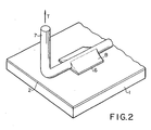
- the heat conductivities of the insulating substrates are measured by using a laser flashing technique, and peeling resistances or peeling strengths are further measured for evaluation of bonding forces between the multi-level surface film structures 2 and the circuit patterns, respectively, by using the fol lowing arrangement.
- a conductive paste formed from a palladium alloy powder containing 20 % silver by weight is screen printed on the insulating substrates P1 to P6 and C1 to C4, and each paste thus printed occupies an area of about 2 millimeters by about 2 millimeters.
- the square shaped paste films are dried at 125 degrees in centigrade for about 10 minutes, and are, then, fired at about 850 degrees in centigrade for about 10 minutes. The firing is repeated nine times so that paste films 6 are produced on the upper surface films 5, respectively. Then, the paste films 6 are subjected to the heat application ten times.
- a generally L-shaped oxygen free copper wire 7 which is soldered to the paste film 6 at about 215 degrees in centigrade.
- the oxygen free copper wire 7 is about 0.9 millimeter in diameter, and a tin-lead eutectic crystal solder 8 is used for bonding.
- the oxygen free copper wire 7 is pulled in a direction indicated by arrow T, and the force is gradually increased until the paste film 6 peels from the insulating substrate.
- the maximum force is divided by the occupying area of the paste film 5, and the force per unit area is defined as "peeling strength".
- the specimens in Tables 1 to 5 have the respective intermediate surface films 4 of the zirconia, however, some substances with small acidities are available, and a titanium oxide, an aluminum oxide, a magnesium oxide, a calcium oxide, a strontium oxide, an yttrium oxide and a barium oxide are the substances with small acidities by way of example.
- a boron oxide, a phosphorus oxide, a germanium oxide, an arsenic oxide, a selenium oxide, a tin oxide, an antimony oxide, a tellurium oxide and a sulfur oxide are of the substance with a large acidity. Any combination between the substance with a small acidity and the substance with a large acidity is advantageous in retarding the consumption of the surface film structure and, accordingly, in the heat conductivity due to reduction in the thickness.
- the insulating substrate according to the present invention is suitable for a hybrid integrated circuit by way of example.
- Fig. 3 shows the structure of a hybrid integrated circuit which is fabricated on an insulating substrate 10 according to the present invention.
- a conductive pattern 11 which provides interconnections between a single chip integrated circuit 12, a resistive pattern 13 and another chip element 14.
- the component elements 12 to 14 thus mounted on the insulating substrate 10 are sealed in a synthetic resin 15, and outer leads are projected from the synthetic resin 13 for communication with an external system (not shown).
- One of the outer leads is shown and designated by reference numeral 16.
- the insulating substrate according to the present invention per se provides a rigid circuit substrate of an electric or electronic circuit, however, a multi-level circuit substrate may be fabricated by using a plurality of insulating substrates according to the present invention. Namely, a circuit pattern is formed on each of the insulating substrates, and a adhesive paste is prepared by mixing a glass powder such as, for example, boron-silicate glass and an organic binder. The adhesive paste is printed on the insulating substrates, and the insulating substrates thus printed with the adhesive paste are laminated to form a multi-level structure. The multi-level structure is heated to a certain temperature over the softening point of the glass powder so that a multi-level circuit substrate is completed.
- a glass powder such as, for example, boron-silicate glass and an organic binder
- a paste is printed on the insulating substrate and, then, fired.
- the paste contains glass frits, and some of the frits have respective basic components, respectively, however, the frits are well known in the person skilled in the art, and, therefore, no further description is incorporated for the sake of simplicity.
- a second embodiment of the present invention is similar in structure to the first embodiment shown in Fig. 1, and, for this reason, the component films and foundation are designated by the same reference numerals in the following description without any detailed description for the sake of simplicity.
- the foundation 1, the lower surface film 3 and the upper surface film 5 are similar in material and thickness to those of the first embodiment, but the intermediate surface film 4 contains not only the zirconia (ZrO2) but also an aluminum oxide (Al2O3).
- the content of the aluminum oxide is larger than about 0.5 % by weight. This is because of the fact that an intermediate surface film with an alumina content less than 0.5 % hardly enhances the adhesion with respect to the lower surface film 3.
- the lower films 3 are produced in a similar manner to those of the first embodiment, and the oxidizing ambiences are described in Table 7.
- Table 7 Reference mark The lower surface film of Al2O3 Oxidation Thickness O2 Press. Vapor Press. Temp. (atm.) (atm.) (deg.) (micron) P11 1.0 1 x 10 ⁇ 5 1350 1.5 P12 ditto ditto ditto 15.0 P13 0.5 1 x 10 ⁇ 4 1400 5.6 P14 ditto ditto ditto 14.0 P15 0.1 1 x 10 ⁇ 3 1450 1.6 P16 ditto ditto ditto 13.2 C11 0.5 1 x 10 ⁇ 4 1400 7.8 C12 0.1 1 x 10 ⁇ 3 1450 6.4
- the intermediate surface films 4 are produced on the respective lower surface films 3 through a sputtering process or a sol-gel process.
- a sputtering process two targets are respectively formed of a sintered zirconia with purity of 99 %, i.e. a sintered complex oxide of alumina and zirconia with zirconia content of about 1 % by weight, and the sintered complex oxide is of a solid solution.
- Each of the targets is about 100 millimeters in diameter and about 10 millimeters in height.
- the targets are selectively installed in an RF sputtering system, and the foundations P11, P13, P15 and C12 covered with the respective lower surface films are confronted with the targets.
- the foundations P11, P13, P15 and C12 are rotated at about 10 rpm, and each sputtering is carried out at about 70 watts for a time period depending upon the thickness of the intermediate surface film 4.
- colloidal solutions are prepared by mixing 500 grams of ethyl alcohol and 250 grams of ethyl silicate and by mixing 1500 grams of isopropyl alcohol, 350 grams of zirconium tetrabutoxyd and 150 grams of aluminium-diisopropyleto-monobutyleto.
- the foundations P12, P14, P16 and C11 thus formed with laminated films are placed in a high temperature atmospheric ambient at about 1000 degrees in centigrade for about 1 hour, then the laminated films are fired so that the intermediate surface films 4 are produced on the respective lower surface films.
- the upper surface films 5 are produced on the respective intermediate surface films 4 in a similar manner to those of the first embodiment, so that the formation process and the thickness of each upper surface film 5 is reported in Table 9.
- the thermal conductivities of the insulating substrates (which are also labeled with the reference marks P11 to P16 and C11 to C12, respectively) are measured by using the laser flashing technique, and peeling resistances or peeling strengths are further measured for evaluation of bonding forces between the multi-level surface film structures 2 and the circuit patterns, respectively, by using the arrangement shown in Fig. 2 under the conditions described in conjunction with the first embodiment.
- Table 10 Reference mark Heat Conductivity Peeling strength (cal/sec. cm. deg) (kg/4 mm2) P11 0.506 4.1 P12 0.515 4.6 P13 0.512 4.7 P14 0.511 4.9 P15 0.506 4.6 P16 0.500 5.1 C11 0.374 4.0 C12 0.354 3.9
- the specimens in Tables 6 to 10 have the respective intermediate surface films 4 each containing the zirconia and the aluminum oxide, however, some substances with small acidities are available, and a titanium oxide, an aluminum oxide, a magnesium oxide, a calcium oxide, a strontium oxide, an yttrium oxide and a barium oxide are the substances with small acidities by way of example.
- a boron oxide, a phosphorus oxide, a germanium oxide, an arsenic oxide, a selenium oxide, a tin oxide, an antimony oxide, a tellurium oxide and a sulfur oxide are of the substance with a large acidity..
- the insulating substrates P11 to P16 according to the present invention are larger in peeling strength than the prior art examples C1 to C3 of Table 5, and each heat conductivity is slightly lowered with respect to those of the prior art examples C1 to C3.
- the present invention is advantageous over the prior art in the peeling strength without any substantial deterioration in heat conductivity.
- the insulating substrates C11 and C12 are not so large in heat conductivity because the intermediate surface films 4 exceeds the recommendable range, i.e. from 0.05 micron to 1 micron in thickness.
- the insulating substrate thus featured by the intermediate surface film 4 of the complex oxide of the zirconia and the alumina is also used for a multi-level insulating substrate as similar to the first embodiment.
- a third embodiment of the present invention is also similar in structure to the first embodiment shown in Fig. 1, and, for this reason, detailed description is omitted for the sake of simplicity, but the components are accompanied with the same reference numerals, respectively.
- the foundation 1 and the lower surface film 3 are similar in the material and in the thickness to those of the first embodiment, and the intermediate surface film 4 is formed of a complex oxide of a zirconia (ZrO2) and an alumina (Al2O3).
- the thickness of the intermediate surface film 4 of the third embodiment is fallen within a range between about 0.05 micron and about 1 micron, and the alumina content is larger than about 0.5 % by weight.
- the reasons for the recommendable thickness and the alumina content are similar to those described in connection with the intermediate surface film of the second embodiment.
- the third embodiment is characterized by the upper surface film 5 which contains a silicon oxide (SiO2) and a boron oxide (B2O3).
- the content of the boron oxide ranges from about 5 % to about 50 % by weight, and the thickness of the upper surface film 5 ranges from about 0.01 micron to about 1 micron.
- the boron oxide is large in acidity and, accordingly, in reactivity with respect to the glass frits, and, therefore, enhances the adhesion of the conductive paste. However, if the content is less than about 5 % by weight, the boron oxide is less effective in view of the enhancement of the adhesion.
- the boron oxide greater than 50 % is unstable in the atmospheric ambient because of vapor contained in the air.
- An upper surface film less than 0.01 micron hardly enhances the adhesion of the circuit pattern 100. If the upper surface film 5 exceeds 1 micron, the insulating substrate hardly propagates heat produced by circuit components, and, therefore, the circuit pattern 100 and the circuits components tend to increase in temperature.
- the lower films 3 are produced in a similar manner to those of the first embodiment, and the oxidizing ambiences are described in Tables 12A and 12B.
- Table 12A Reference mark The lower surface film of Al2O3 Oxidation Thickness O2 Press. Vapor Press. Temp.
- the intermediate surface films 4 are produced on the respective lower surface films 3 through a sputtering process or a sol-gel process.
- a target of a sintered zirconia (ZrO2) with a purity of 99 % i.e. a target of a sintered zirconia (ZrO2) with a purity of 99 %, a target of a sintered oxide of alumina and zirconia with alumina content about 1 % by weight, a target of a sintered oxide of alumina and zirconia with alumina content of about 20 % by weight, and a sintered oxide of alumina and zirconia with alumina content of about 38 % by weight.
- the sintered oxides are of a solid solution.
- Each of the targets is about 100 millimeters in diameter and about 10 millimeters in height.
- the targets are selectively installed in an RF sputtering system, and the foundations P24, P26, P28, P32, P33, C23, C26 and C30 covered with the respective lower surface films are confronted with the targets.
- the foundations P24, P26, P28, P32, P33, C23, C26 and C30 are rotated at about 10 rpm, and each sputtering is carried out at about 70 watts for a time period depending upon the thickness of the intermediate surface film 4.
- colloidal solutions are prepared by mixing a first solution of 1500 grams of isopropyl alcohol and 600 grams of zirconium tetrabutoxyd and a second solution of 1500 grams of isopropyl alcohol and 150 grams of aluminium-diisopropyletomonobutyleto.
- the upper surface films 5 are produced on the respective intermediate surface films 4 by using either sputtering or sol-gel technique.
- three targets are prepared, i.e. a target of a sintered silicon dioxide with a purity of 99.9 %, a target of a sintered product of silica (SiO2) and a boron oxide (B2O3) with silica content of about 10 % by weight, and a target of a sintered product of the silica and the boron oxide with silica content of about 30 % by weight.
- the sintered products are of a solid solution.
- Each of the targets is about 100 millimeters in diameter and about 10 millimeters in height.
- the targets are selectively installed in an RF sputtering system, and the foundations P21, P25, P27, P28, P33, C24 to C26 and C33 covered with the respective intermediate surface films are confronted with the targets.
- the foundations P21, P25, P27, P28, P33, C24 to C26 and C31 are rotated at about 10 rpm, and each sputtering is carried out at about 100 watts for a certain time period depending upon the thickness of the upper surface film 5.
- colloidal solutions are prepared by mixing a first solution of 500 grams of ethyl alcohol and 250 grams of ethyl silicate and a second solution of 500 grams of ethyl alcohol and 100 grams of triethoxyborane.
- the foundations P22 to P24, P26, P29 to P32, C22, C23 and C27 to C32 thus formed with laminated films are placed in a high temperature atmospheric ambient at about 1000 degrees in centigrade for about 1 hour, then the laminated films are fired so that the upper surface films 5 are produced on the respective intermediate surface films 4 or directly on the foundations 1.
- the formation of the upper films 5 are summarized in Tables 9A and 9B.
- Table 14A Reference mark The upper surface film Process Compositon (WT%) Thickness B2O3 SiO2 (micron) P21 Sputtering 10.2 Residual 0.01 P22 Sol-gel 5.1 Residual 0.24 P23 Sol-gel 25.1 Residual 0.68 P24 Sol-gel 49.2 Residual 0.92 P25 Sputtering 30.1 Residual 1.00 P26 Sol-gel 5.5 Residual 0.02 P27 Sputtering 29.0 Residual 0.09 P28 Sputtering 10.3 Residual 0.13 P29 Sol-gel 24.6 Residual 0.70 P30 Sol-gel 32.4 Residual 0.62 P31 Sol-gel 42.4 Residual 0.45 P32 Sol-gel 49.6 Residual 0.31 P33 Sputtering 30.3 Residual 0.20 Table 14B Reference mark The upper surface film Process Compositon (WT%) Thickness B2O3 SiO2 (
- the thermal conductivities of the insulating substrates are measured by using the laser flashing technique, and peeling resistances or peeling strengths are further measured for evaluation of bonding forces between the multi-level surface film structures 2 and the circuit patterns, respectively, by using the arrangement shown in Fig. 2.
- the thermal conductivities and the peeling resistances are measured immediately after the formation of the first conductive films and after the completion of the conductive patterns, respectively.
- Table 15A (1st film) Reference mark Heat Conductivity Peeling strength (cal/sec. cm. deg) (kg/4 mm2) P21 0.621 4.0 P22 0.601 4.3 P23 0.587 4.5 P24 0.512 4.9 P25 0.410 5.1 P26 0.611 5.0 P27 0.602 4.7 P28 0.596 4.2 P29 0.588 4.3 P30 0.444 4.2 P31 0.561 4.5 P32 0.531 4.4 P33 0.431 4.3
- Table 15B (pattern) Reference mark Heat Conductivity Peeling strength (cal/sec. cm.
- the specimens in Tables 11A to 15D have the respective intermediate surface films 4 containing the zirconia and the alumina, however, some substances with small acidities are available, and a titanium oxide, an aluminum oxide, a magnesium oxide, a calcium oxide, a strontium oxide, an yttrium oxide and a barium oxide are the substances with small acidities by way of example.
- the upper surface film 5 is formed of a substance with a larger acidity than the substance used for formation of the intermediate surface film 4, and a boron oxide, a phosphorus oxide, a germanium oxide, an arsenic oxide, a selenium oxide, a tin oxide, an antimony oxide, a tellurium oxide and a sulfur oxide are available.
- the insulating substrate of the third embodiment is also used for fabrication of a multi-level insulating substrate as similar to the first embodiment.
- the intermediate surface film 4 is effective against the penetration of the melted frits without increasing the total thickness of the intermediate and upper surface films.
- the insulating substrates according to the present invention are as large in heat conductivity as those without any lower and intermediate surface films, and are improved in the peeling strength.
- the insulating substrate according to the present invention is a little bit expensive rather than those disclosed in the U.S. Patent Application filed on February 5, 1990, the insulating substrate of the present invention is much advantageous in hte peeling strength under repetition of firing stage without sacrifice of the heat conductivity.
Landscapes
- Engineering & Computer Science (AREA)
- Manufacturing & Machinery (AREA)
- Microelectronics & Electronic Packaging (AREA)
- Parts Printed On Printed Circuit Boards (AREA)
- Inorganic Insulating Materials (AREA)
- Non-Metallic Protective Coatings For Printed Circuits (AREA)
Applications Claiming Priority (4)
| Application Number | Priority Date | Filing Date | Title |
|---|---|---|---|
| JP128285/89 | 1989-05-22 | ||
| JP12828589A JP2591158B2 (ja) | 1989-05-22 | 1989-05-22 | 放熱性のすぐれた半導体装置用基板 |
| JP28924389A JP2623868B2 (ja) | 1989-11-07 | 1989-11-07 | 放熱性のすぐれた半導体装置用基板素材 |
| JP289243/89 | 1989-11-07 |
Publications (3)
| Publication Number | Publication Date |
|---|---|
| EP0399265A2 true EP0399265A2 (de) | 1990-11-28 |
| EP0399265A3 EP0399265A3 (de) | 1992-03-25 |
| EP0399265B1 EP0399265B1 (de) | 1995-01-18 |
Family
ID=26464004
Family Applications (1)
| Application Number | Title | Priority Date | Filing Date |
|---|---|---|---|
| EP90108447A Expired - Lifetime EP0399265B1 (de) | 1989-05-22 | 1990-05-04 | Substrat, verwendbar bei der Herstellung einer Dickschichtschaltung |
Country Status (4)
| Country | Link |
|---|---|
| US (1) | US5087509A (de) |
| EP (1) | EP0399265B1 (de) |
| KR (1) | KR900019179A (de) |
| DE (1) | DE69016096T2 (de) |
Families Citing this family (10)
| Publication number | Priority date | Publication date | Assignee | Title |
|---|---|---|---|---|
| DE4030055A1 (de) * | 1990-09-22 | 1992-03-26 | Bosch Gmbh Robert | Verfahren zum herstellen einer schaltung |
| US6207288B1 (en) | 1991-02-05 | 2001-03-27 | Cts Corporation | Copper ink for aluminum nitride |
| US5399239A (en) * | 1992-12-18 | 1995-03-21 | Ceridian Corporation | Method of fabricating conductive structures on substrates |
| US5466488A (en) * | 1993-02-08 | 1995-11-14 | Mitsubishi Materials Corporation | Method of making glazed AlN substrate with an Al2 O3 -SiO2 interfacial layer |
| US7875871B2 (en) | 2006-03-31 | 2011-01-25 | Sandisk 3D Llc | Heterojunction device comprising a semiconductor and a resistivity-switching oxide or nitride |
| US8233308B2 (en) | 2007-06-29 | 2012-07-31 | Sandisk 3D Llc | Memory cell that employs a selectively deposited reversible resistance-switching element and methods of forming the same |
| US20090104756A1 (en) * | 2007-06-29 | 2009-04-23 | Tanmay Kumar | Method to form a rewriteable memory cell comprising a diode and a resistivity-switching grown oxide |
| US7824956B2 (en) | 2007-06-29 | 2010-11-02 | Sandisk 3D Llc | Memory cell that employs a selectively grown reversible resistance-switching element and methods of forming the same |
| US9703335B2 (en) * | 2013-01-14 | 2017-07-11 | Dell Products L.P. | Information handling system chassis with anisotropic conductance |
| CN104185365B (zh) * | 2013-05-23 | 2018-06-26 | 比亚迪股份有限公司 | 一种线路板及其制备方法 |
Family Cites Families (14)
| Publication number | Priority date | Publication date | Assignee | Title |
|---|---|---|---|---|
| JPS5439579A (en) * | 1977-09-02 | 1979-03-27 | Fujitsu Ltd | Semiconductor device of field effect type |
| US4153518A (en) * | 1977-11-18 | 1979-05-08 | Tektronix, Inc. | Method of making a metalized substrate having a thin film barrier layer |
| JPS5922399B2 (ja) * | 1981-10-14 | 1984-05-26 | 日本電気株式会社 | 多層セラミツク基板 |
| JPS58101442A (ja) * | 1981-12-11 | 1983-06-16 | Hitachi Ltd | 電気的装置用基板 |
| JPS58202408A (ja) * | 1982-05-20 | 1983-11-25 | Nippon Soken Inc | 熱線反射膜 |
| DE3247985C2 (de) * | 1982-12-24 | 1992-04-16 | W.C. Heraeus Gmbh, 6450 Hanau | Keramischer Träger |
| US4582745A (en) * | 1984-01-17 | 1986-04-15 | Rca Corporation | Dielectric layers in multilayer refractory metallization structure |
| EP0153737B1 (de) * | 1984-02-27 | 1993-07-28 | Kabushiki Kaisha Toshiba | Schaltungssubstrat mit hoher Wärmeleitfähigkeit |
| US4695517A (en) * | 1985-05-31 | 1987-09-22 | Ngk Spark Plug Co., Ltd. | Composite layer aluminum nitride base sintered body |
| US4950588A (en) * | 1985-07-10 | 1990-08-21 | Molecular Diagnostics, Inc. | Prolonged enhanced chemiluminescence |
| US4810563A (en) * | 1986-03-14 | 1989-03-07 | The Bergquist Company | Thermally conductive, electrically insulative laminate |
| EP0327068B1 (de) * | 1988-02-01 | 1995-08-30 | Mitsubishi Materials Corporation | Substrat zum Herstellen einer Dickschichtschaltung |
| US4908348A (en) * | 1988-02-08 | 1990-03-13 | Eastman Kodak Company | Barrier layer arrangement for conductive layers on silicon substrates |
| DE69000112D1 (de) * | 1989-02-03 | 1992-07-02 | Mitsubishi Materials Corp | Substrat zur herstellung eines dickschichtschaltkreises. |
-
1990
- 1990-05-04 DE DE69016096T patent/DE69016096T2/de not_active Expired - Fee Related
- 1990-05-04 EP EP90108447A patent/EP0399265B1/de not_active Expired - Lifetime
- 1990-05-18 US US07/524,936 patent/US5087509A/en not_active Expired - Fee Related
- 1990-05-22 KR KR1019900007378A patent/KR900019179A/ko not_active Abandoned
Also Published As
| Publication number | Publication date |
|---|---|
| KR900019179A (ko) | 1990-12-24 |
| DE69016096T2 (de) | 1995-06-14 |
| EP0399265B1 (de) | 1995-01-18 |
| EP0399265A3 (de) | 1992-03-25 |
| DE69016096D1 (de) | 1995-03-02 |
| US5087509A (en) | 1992-02-11 |
Similar Documents
| Publication | Publication Date | Title |
|---|---|---|
| EP0153737B1 (de) | Schaltungssubstrat mit hoher Wärmeleitfähigkeit | |
| US4861646A (en) | Co-fired metal-ceramic package | |
| JP2765885B2 (ja) | 窒化アルミニウム回路基板及びその製造方法 | |
| US4940849A (en) | Metallizing paste | |
| US4835039A (en) | Tungsten paste for co-sintering with pure alumina and method for producing same | |
| KR900005842B1 (ko) | 질화 알루미늄 기판 | |
| US5306679A (en) | Heat conductive colored aluminum nitride sintered body | |
| EP0399265A2 (de) | Substrat, verwendbar bei der Herstellung einer Dickschichtschaltung | |
| EP0202858B1 (de) | Keramische Platte für Mehrschichtschaltungsverbindungen und Verfahren zum Herstellen derselben | |
| EP0196670B1 (de) | Keramisches Substrat für mikroelektronische Schaltungen und Verfahren zu deren Herstellung | |
| EP0230675B1 (de) | Keramiksubstrat für Zuleitungen und Verfahren zu seiner Herstellung | |
| US5096768A (en) | Substrate used for fabrication of thick film circuit | |
| KR930005894B1 (ko) | 금속화층이 형성된 질화알루미늄 소결체 및 이의 제조방법 | |
| JP2598872B2 (ja) | ガラスセラミックス多層基板 | |
| Horiuchi et al. | New mullite ceramic packages and substrates | |
| EP0327068B1 (de) | Substrat zum Herstellen einer Dickschichtschaltung | |
| JPH01317183A (ja) | 低熱膨張基板用メタライズ組成物 | |
| JPH0725617B2 (ja) | 窒化アルミニウム基板およびその製造方法 | |
| US5292552A (en) | Method for forming metallized layer on an aluminum nitride sintered body | |
| JP3450998B2 (ja) | 配線基板およびその実装構造 | |
| US5830570A (en) | Aluminum nitride substrate and process for preparation thereof | |
| JP3450167B2 (ja) | 半導体素子収納用パッケージ | |
| JPH11343178A (ja) | 銅板と非酸化物セラミックスとの接合方法 | |
| JPH0633206B2 (ja) | メタライズ組成物 | |
| JPS62186407A (ja) | 導電性組成物 |
Legal Events
| Date | Code | Title | Description |
|---|---|---|---|
| PUAI | Public reference made under article 153(3) epc to a published international application that has entered the european phase |
Free format text: ORIGINAL CODE: 0009012 |
|
| AK | Designated contracting states |
Kind code of ref document: A2 Designated state(s): BE DE FR GB NL |
|
| 17P | Request for examination filed |
Effective date: 19901228 |
|
| RAP1 | Party data changed (applicant data changed or rights of an application transferred) |
Owner name: MITSUBISHI MATERIALS CORPORATION |
|
| PUAL | Search report despatched |
Free format text: ORIGINAL CODE: 0009013 |
|
| AK | Designated contracting states |
Kind code of ref document: A3 Designated state(s): BE DE FR GB NL |
|
| 17Q | First examination report despatched |
Effective date: 19930820 |
|
| GRAA | (expected) grant |
Free format text: ORIGINAL CODE: 0009210 |
|
| AK | Designated contracting states |
Kind code of ref document: B1 Designated state(s): BE DE FR GB NL |
|
| PG25 | Lapsed in a contracting state [announced via postgrant information from national office to epo] |
Ref country code: NL Effective date: 19950118 Ref country code: BE Effective date: 19950118 |
|
| REF | Corresponds to: |
Ref document number: 69016096 Country of ref document: DE Date of ref document: 19950302 |
|
| ET | Fr: translation filed | ||
| NLV1 | Nl: lapsed or annulled due to failure to fulfill the requirements of art. 29p and 29m of the patents act | ||
| PLBE | No opposition filed within time limit |
Free format text: ORIGINAL CODE: 0009261 |
|
| STAA | Information on the status of an ep patent application or granted ep patent |
Free format text: STATUS: NO OPPOSITION FILED WITHIN TIME LIMIT |
|
| 26N | No opposition filed | ||
| PGFP | Annual fee paid to national office [announced via postgrant information from national office to epo] |
Ref country code: FR Payment date: 19960430 Year of fee payment: 7 |
|
| PGFP | Annual fee paid to national office [announced via postgrant information from national office to epo] |
Ref country code: GB Payment date: 19960501 Year of fee payment: 7 |
|
| PGFP | Annual fee paid to national office [announced via postgrant information from national office to epo] |
Ref country code: DE Payment date: 19960731 Year of fee payment: 7 |
|
| PG25 | Lapsed in a contracting state [announced via postgrant information from national office to epo] |
Ref country code: GB Effective date: 19970504 |
|
| GBPC | Gb: european patent ceased through non-payment of renewal fee |
Effective date: 19970504 |
|
| PG25 | Lapsed in a contracting state [announced via postgrant information from national office to epo] |
Ref country code: FR Free format text: LAPSE BECAUSE OF NON-PAYMENT OF DUE FEES Effective date: 19980130 |
|
| PG25 | Lapsed in a contracting state [announced via postgrant information from national office to epo] |
Ref country code: DE Free format text: LAPSE BECAUSE OF NON-PAYMENT OF DUE FEES Effective date: 19980203 |
|
| REG | Reference to a national code |
Ref country code: FR Ref legal event code: ST |