EP0399738A2 - Convertisseur analogique-numérique - Google Patents
Convertisseur analogique-numérique Download PDFInfo
- Publication number
- EP0399738A2 EP0399738A2 EP90305436A EP90305436A EP0399738A2 EP 0399738 A2 EP0399738 A2 EP 0399738A2 EP 90305436 A EP90305436 A EP 90305436A EP 90305436 A EP90305436 A EP 90305436A EP 0399738 A2 EP0399738 A2 EP 0399738A2
- Authority
- EP
- European Patent Office
- Prior art keywords
- analogue
- bandpass filter
- digital converter
- output
- filter means
- Prior art date
- Legal status (The legal status is an assumption and is not a legal conclusion. Google has not performed a legal analysis and makes no representation as to the accuracy of the status listed.)
- Withdrawn
Links
- 238000012937 correction Methods 0.000 claims abstract description 17
- 239000003990 capacitor Substances 0.000 claims abstract description 9
- 238000005070 sampling Methods 0.000 claims description 64
- 230000003111 delayed effect Effects 0.000 claims description 10
- 238000001914 filtration Methods 0.000 claims description 4
- 238000010586 diagram Methods 0.000 description 8
- 238000007493 shaping process Methods 0.000 description 5
- 230000008901 benefit Effects 0.000 description 3
- 230000000630 rising effect Effects 0.000 description 3
- 238000001228 spectrum Methods 0.000 description 3
- 238000012545 processing Methods 0.000 description 2
- 239000013078 crystal Substances 0.000 description 1
- 238000013461 design Methods 0.000 description 1
- 230000000694 effects Effects 0.000 description 1
- 238000012986 modification Methods 0.000 description 1
- 230000004048 modification Effects 0.000 description 1
- 238000010079 rubber tapping Methods 0.000 description 1
- 238000012546 transfer Methods 0.000 description 1
Images


Classifications
-
- H—ELECTRICITY
- H03—ELECTRONIC CIRCUITRY
- H03M—CODING; DECODING; CODE CONVERSION IN GENERAL
- H03M3/00—Conversion of analogue values to or from differential modulation
- H03M3/30—Delta-sigma modulation
- H03M3/322—Continuously compensating for, or preventing, undesired influence of physical parameters
- H03M3/324—Continuously compensating for, or preventing, undesired influence of physical parameters characterised by means or methods for compensating or preventing more than one type of error at a time, e.g. by synchronisation or using a ratiometric arrangement
- H03M3/326—Continuously compensating for, or preventing, undesired influence of physical parameters characterised by means or methods for compensating or preventing more than one type of error at a time, e.g. by synchronisation or using a ratiometric arrangement by averaging out the errors
- H03M3/328—Continuously compensating for, or preventing, undesired influence of physical parameters characterised by means or methods for compensating or preventing more than one type of error at a time, e.g. by synchronisation or using a ratiometric arrangement by averaging out the errors using dither
- H03M3/3283—Continuously compensating for, or preventing, undesired influence of physical parameters characterised by means or methods for compensating or preventing more than one type of error at a time, e.g. by synchronisation or using a ratiometric arrangement by averaging out the errors using dither the dither being in the time domain
-
- H—ELECTRICITY
- H03—ELECTRONIC CIRCUITRY
- H03M—CODING; DECODING; CODE CONVERSION IN GENERAL
- H03M3/00—Conversion of analogue values to or from differential modulation
- H03M3/30—Delta-sigma modulation
- H03M3/39—Structural details of delta-sigma modulators, e.g. incremental delta-sigma modulators
- H03M3/402—Arrangements specific to bandpass modulators
- H03M3/404—Arrangements specific to bandpass modulators characterised by the type of bandpass filters used
- H03M3/408—Arrangements specific to bandpass modulators characterised by the type of bandpass filters used by the use of an LC circuit
-
- H—ELECTRICITY
- H03—ELECTRONIC CIRCUITRY
- H03M—CODING; DECODING; CODE CONVERSION IN GENERAL
- H03M3/00—Conversion of analogue values to or from differential modulation
- H03M3/30—Delta-sigma modulation
- H03M3/39—Structural details of delta-sigma modulators, e.g. incremental delta-sigma modulators
- H03M3/412—Structural details of delta-sigma modulators, e.g. incremental delta-sigma modulators characterised by the number of quantisers and their type and resolution
- H03M3/422—Structural details of delta-sigma modulators, e.g. incremental delta-sigma modulators characterised by the number of quantisers and their type and resolution having one quantiser only
- H03M3/43—Structural details of delta-sigma modulators, e.g. incremental delta-sigma modulators characterised by the number of quantisers and their type and resolution having one quantiser only the quantiser being a single bit one
-
- H—ELECTRICITY
- H03—ELECTRONIC CIRCUITRY
- H03M—CODING; DECODING; CODE CONVERSION IN GENERAL
- H03M3/00—Conversion of analogue values to or from differential modulation
- H03M3/30—Delta-sigma modulation
- H03M3/39—Structural details of delta-sigma modulators, e.g. incremental delta-sigma modulators
- H03M3/436—Structural details of delta-sigma modulators, e.g. incremental delta-sigma modulators characterised by the order of the loop filter, e.g. error feedback type
- H03M3/438—Structural details of delta-sigma modulators, e.g. incremental delta-sigma modulators characterised by the order of the loop filter, e.g. error feedback type the modulator having a higher order loop filter in the feedforward path
- H03M3/454—Structural details of delta-sigma modulators, e.g. incremental delta-sigma modulators characterised by the order of the loop filter, e.g. error feedback type the modulator having a higher order loop filter in the feedforward path with distributed feedback, i.e. with feedback paths from the quantiser output to more than one filter stage
Definitions
- This invention relates to analogue-to-digital converters.
- the invention is particularly but not exclusively concerned with digital implementation of some of the stages of a radio receiver, and an aim is to achieve a highly linear, high resolution output.
- analogue-to-digital converter it is desirable to have the analogue-to-digital converter as near the front end of the receiver as possible to obtain the benefits of subsequent digital processing but as a practical matter often the earliest this can be done is at a suitable intermediate frequency (i.f.) stage.
- a suitable intermediate frequency (i.f.) stage For example, this could be a frequency of 2.5MHz with a bandwidth of 100kHz.
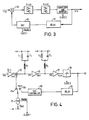
- the applicants have proposed to use a Sigma-Delta noise shaping analogue-to-digital converter (Figure 1) for this purpose.
- the converter includes a bandpass analogue filter H(s) which feeds a quantiser Q for converting the analogue signal X (s) to one of a discrete number of levels which are sampled by a sampler.
- a digital-to-analogue converter is included in a feedback loop to an adder in which the analogue output strives to follow the input signal to the coder within the passband of the filter.
- Y(z) is the digital output.
- a digital noise shaping circuit was considered i.e. digital filter, quantiser and adder, and omitting the digital-to-analogue converter from the feedback path.
- the i.f. signal must be sampled and digitised to be fed to the noise shaping coder, and the necessary analogue-to-digital converter would be multi-bit and therefore potentially non-linear.
- an analogue sampled data circuit was considered utilising a sampled data analogue filter, quantiser, digital-to-analogue converter and analogue adder. While this reduced the size and power consumption of the converter and avoided the need for a multi-bit A-D converter, as in the digital implementation, distortions could still arise from the jitter on the input sample and hold circuit and distortions in the sampled data filter.
- the impulse response would be finite at odd sampling instants T, 3T, 5T etc, and would be alternatively positive and negative. If even sampling instants corresponded to an I component and odd sampling instants corresponded to a Q component, the fedback pulse corresponding to an I data output pulse, would superimpose an alternating signal on Q data output pulses. The tendency to have a natural resonant frequency could thus result in instability.
- the invention provides an analogue-to-digital converter comprising bandpass filter means for filtering a signal derived from an analogue input signal, digitising means for producing samples at one of a discrete number of values corresponding to a signal derived from the output of the bandpass filter means, a feedback loop for feeding a signal derived from the output of the digitising means to the bandpass filter means, the circuit being arranged to produce in operation a minimum in the quantisation noise in the passband of the filter means, and in which at least some of the zero crossings of the response of the band pass filter means to a single fedback pulse are made to coincide with the sampling instants.
- means may be provided to produce a phase offset between the feedback pulses and the sampling instants of the digitising means.
- the zero crossings could be made to coincide by displacing the response curve relative to the grid of sampling instants, or vice versa.
- the desired samples between the zero crossing samples would not lie exactly at the respective peaks of the impulse response.
- a small error here in a sampling instant would make only a very small error in the error amplitude since the peaks have only a small slope at these regions.
- a corrective feedback loop may be provided for feeding correction pulses derived from the output of the digitising means to the bandpass filter means.
- the zero crossings are made to coincide with the sampling instants by cancellation of the non-zero component at the sampling instants by the correction pulses.
- the bandpass filter means may be in two stages, each stage of which may comprise an inductor, capacitor, and resistor which may be fed with current and produce an output voltage signal.
- the digitising means may produce samples at one of two values, and could include a comparator arranged to produce a positive or negative voltage output.
- the first analogue-to-digital converter has an input i/p for analogue signals such as the i.f. of a radio receiver and the output o/p producing data in digitised form.
- the converter has analogue bandpass filter means in two stages H1(s) and H2(s). These are followed by a quantiser which converts the analogue signal into one of a number of discrete levels, the output of the quantiser being sampled at a sampling frequency of 10MHz provided by clock 3, i.e. a sampling period of 100ns.
- the digitised data pulses are fed back to the input of the bandpass filter means by a main feedback loop, by a delay 1, a digital-to-analogue converter 2 and an adder 3.
- the i.f. signal consists of an I(in phase) and Q(quadrature) component. It was found that the digital output corresponding to the Q component was influenced by variations in the I component (and vice versa). Naturally, the coder should modulate the I and Q components in the analogue signal entirely independently.
- the open loop impulse response of the bandpass filter means of Figure 3 is of the general form shown in the Figure.
- T is the sampling period
- This could be looked at in another way by appreciating that the original impulse centred on t 0 contains only cosine components, and that the response of the filter must therefore contain only cosine terms and no sine terms.
- a suitable digital response for a digital filer would be 2, 0, -3, 0, 4, 0, -5, 0 and so on.
- the instability referred to arises because the response of the bandpass filter means does not exactly pass through 0 at times t T, 3T, 5T. This is not because of limitations inherent in the components.
- means for varying the phase between clocks 1 and 3.
- the analogue input to the bandpass filters H1(s) and H2(s) is sampled by the quantiser producing a digital data output.
- This string of pulses is delayed by one and a half periods by the delay 21, clocked by a clock running in synchronism with clock 2.
- the data is fed to digital-to-analogue converter 22 which is enabled by clock 1, and produces feedback pulses.
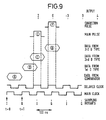
- Adjustments are made to the relative phases of clocks 1 and 2 so that the feedback pulses (controlled by clock 1) are advanced or retarded relative to the data pulses and hence relative to the sampling instants (controlled by clock 2) until the zero crossings of the open loop impulse response shown in Figure 2 coincide with the sampling instants. While the coincidence of the crossings cannot be measured or calculated directly, the need for any phase variation is indicated by examination of the spectra of the converter in the sense that non-coincidence of the zero crossings with the sampling instance will be manifested as unwanted peaks P in the spectra e.g. as shown in Figure 5a. The phase relationship of the two clocks can then be varied to eliminate the unwanted peak. A full 360° of variation of phase relationship between clocks 1 and 2 is built into the system in order to cope with any possible phase adjustment necessary.
- the effect of adjusting the phase relationship of the two clocks is to move the impulse response curve (by adjusting clock 1) or the grid of sampling instants (by adjusting clock 2). It follows that the peaks of the impulse response will not coincide with the sampling instants. However, because the gradient of the impulse response is much larger at the zero crossings than at the peaks, it is possible, by altering the relative phases of the impulse response and the sampling instants, to eliminate a large error at the zero crossings whilst introducing only a small error at the peaks.
- the quantiser may be a multi-bit quantiser e.g. two bits i.e. two positive and two negative values.
- a one bit quantiser is used i.e. a positive or a negative value.
- the use of a one bit quantiser has the advantage that the quantisation will then be linear, and the digital-to-analogue converter then simply produces a pair of output levels of very consistent value in response to a digital input comprising two ranges of levels, one range designated as digital 0 and one range designated as digital 1.
- the bandpass filter means may be an inductor and a capacitor in parallel, together with a series resistive element.
- the analogue input voltage is fed to an input buffer 24 having a high output impedance, the output signal being a current to allow the addition at summing node current adder 25.
- the loop filters H1(s), H2(s) are implemented by inductors and capacitors, which may be similar elements such as crystal resonators, together with resistors, as shown.
- Buffer amplifier 26 converts the output voltage of the first filter to a current drive of the second filter.
- Buffer 27 provides a voltage input to a comparator which has a positive and a negative output level depending on whether the input voltage is positive or negative at the sampling instants defined by the clock 2.
- Delay 29, clocked by clock 2 provides a one and a half period delay.
- Digital-to-analogue converter controller 30 connects the output of current generator 31 to contact 31a when data pulses are positive (see Figure 5) so that feedback pulses are enabled by clock 1, and to contact 31b connected to earth when data pulses are a negative level.
- the phase relationship of clocks 1 and 2 is adjusted as described. Of course, once the adjustment has been made and suitable component values selected, subsequent converters can be made without the phase relationship being variable but simply at the particular phase relationship found to give best results reducing instability.
- Suitable values of components must be chosen to give an open loop response such that at the even sampling instants, 0, 2T, 4T etc, the response coincides with those of a digitally implemented filter i.e. 2, -3, 4, -5 etc.
- phase relationship of clocks 1 and 2 there may be a fixed relationship between the phases of the clocks 1 and 2, and the zero crossings may be brought into synchronism with the sampling instants by cancellation of any non-zero component by correction pulses.
- a correction feedback loop contains a delay 4 and digital-to-analogue converters 5 to 7 feeding adders 8 to 10.
- the main feedback data pulses travelling via the delay 1 are delayed one and a half periods in a fixed phase relationship relative to the data pulses at the output, and the correction data pulses are delayed by a further sample period.
- the level of the correction pulses are varied so that any non-zero component of the impulse response at the sampling instants is cancelled by an equal and opposite component.
- the bandpass filter may be realised by an inductor and capacitor in parallel, together with series resistors, the quantiser may be a multi-bit but preferably a single bit quantiser, and the null in quantisation noise may be at one quarter of the sampling frequency of 10 MHz.
- the input of the loop filters is a current signal and the output is a voltage signal.
- the main feedback pulse and the correction pulses are provided by current generators controlled by the data output of the converter. Consequently, current adders may be employed. Because balanced inputs are employed, the same current source is used for positive and negative main and correction pulses. Unbalanced filters could be used if desired by either pulsing the correction DAC (I1 or I2) or not.
- the pulse level of I1 or I2 will need to be scaled to the appropriate output bit level.
- the converter achieves high resolution within the passband of the loop filters by the use of over-sampling (of the sampling frequency relative to the bandwidth) and feedback.
- the sampling rate is four times the centre frequency of the passband.
- the loop filters are tuned at or close to the centre frequency.
- the input signal is fed to an input buffer 11 having a non-inverting output and an inverting output.
- the output impedance is very high, and the output signals are current rather than voltage signals to allow addition in the current adders 3a, 3b.
- the loop filters H1(s) and H2(s) each have an inductor (L) in parallel with a capacitor (C), the inductors being tapped and fed with current via pairs of resistors r1, r2, respectively, the values being chosen so that, with the correction pulses, the open loop response of the bandpass filter means coincides with that of an ideal digital filter e.g. 2, -3, 4, -5 ... at the even sampling instants.
- the output of the first stage is a voltage fed to a mid-stage buffer amplifier 12 with a high input and output impedance which serves to isolate the two loop filters from each other.
- the output of the buffer amplifier forms a current drive to adders 9a, 9b at the input of the second loop filter.
- the output of the second loop filter is connected to a sampled quantiser formed by a comparator with a low delay and low hysteresis, which acts as a one-bit analogue-to-digital converter, i.e. two voltage levels.
- the comparator output changes to the appropriate positive or negative voltage every rising clock pulse edge.
- the flip-flops 13, 15 transfer the input voltage from the D to the Q terminal on each rising clock edge, providing a one pulse period delay or, in the case of flip-flop 14, a half period delay because the falling edge has been inverted to become a rising edge.
- the main feedback pulses could be delayed by another even number of periods instead of 2, e.g. 4, 6 and the correction pulses (in Figures 6 and 7) could be delayed by another odd number of periods instead of 3.
- the filters could employ series inductance and capacitance instead of parallel inductance and capacitance, and in this case resistors in parallel with the inductor and capacitor in series may be used. Equally, other high-Q filters could be used in all embodiments.
Landscapes
- Engineering & Computer Science (AREA)
- Theoretical Computer Science (AREA)
- Compression, Expansion, Code Conversion, And Decoders (AREA)
- Analogue/Digital Conversion (AREA)
Applications Claiming Priority (4)
| Application Number | Priority Date | Filing Date | Title |
|---|---|---|---|
| GB8912137 | 1989-05-26 | ||
| GB8912137A GB2232022A (en) | 1989-05-26 | 1989-05-26 | Analogue-to-digital converter |
| GB9009197 | 1990-04-24 | ||
| GB9009197A GB2232023B (en) | 1989-05-26 | 1990-04-24 | Analogue to digital converter |
Publications (2)
| Publication Number | Publication Date |
|---|---|
| EP0399738A2 true EP0399738A2 (fr) | 1990-11-28 |
| EP0399738A3 EP0399738A3 (fr) | 1991-05-08 |
Family
ID=26295404
Family Applications (1)
| Application Number | Title | Priority Date | Filing Date |
|---|---|---|---|
| EP19900305436 Withdrawn EP0399738A3 (fr) | 1989-05-26 | 1990-05-18 | Convertisseur analogique-numérique |
Country Status (4)
| Country | Link |
|---|---|
| US (1) | US5027120A (fr) |
| EP (1) | EP0399738A3 (fr) |
| JP (1) | JPH0396019A (fr) |
| AU (1) | AU624298B2 (fr) |
Cited By (11)
| Publication number | Priority date | Publication date | Assignee | Title |
|---|---|---|---|---|
| EP0495328A1 (fr) * | 1991-01-15 | 1992-07-22 | International Business Machines Corporation | Convertisseur sigma delta |
| EP0520617A3 (en) * | 1991-06-01 | 1993-08-18 | Gec-Marconi Limited | Analogue-to-digital converters |
| WO1993021691A1 (fr) * | 1992-04-08 | 1993-10-28 | Gec-Marconi Limited | Convertisseur analogique-numerique |
| FR2707815A1 (fr) * | 1993-07-13 | 1995-01-20 | Alcatel Mobile Comm France | Convertisseur analogique numérique à boucle de contre-réaction modulée. |
| EP0543618A3 (fr) * | 1991-11-20 | 1995-05-31 | Marconi Gec Ltd | |
| EP1166437A4 (fr) * | 1999-03-09 | 2002-08-14 | Tripath Technology Inc | Etage d'attaque de ligne a haut rendement |
| WO2003052939A3 (fr) * | 2001-12-18 | 2004-01-22 | Koninkl Philips Electronics Nv | Numériseur sigma delta à convertisseur firdac |
| WO2010018533A3 (fr) * | 2008-08-13 | 2010-04-08 | Koninklijke Philips Electronics N.V. | Circuit de conversion analogique/numérique avec détermination automatique du point de polarisation et systèmes à gradient rm utilisant celui-ci |
| WO2010049504A1 (fr) * | 2008-10-31 | 2010-05-06 | Thales | Procede de controle du retard de boucle dans un modulateur sigma-delta et modulateur mettant en œuvre le procede |
| US20230308111A1 (en) * | 2022-03-23 | 2023-09-28 | Silicon Laboratories Inc. | Analog-to-Digital Converter Having Punctured Quantizer |
| US12512852B2 (en) | 2023-08-23 | 2025-12-30 | Silicon Laboratories Inc. | Noise-shaping converter with digital modulator |
Families Citing this family (33)
| Publication number | Priority date | Publication date | Assignee | Title |
|---|---|---|---|---|
| JP3048452B2 (ja) * | 1990-11-30 | 2000-06-05 | 株式会社東芝 | Ad変換器 |
| GB9109637D0 (en) * | 1991-05-03 | 1991-06-26 | Marconi Gec Ltd | Analogue-to-digital and digital-to-analogue converters |
| US5179380A (en) * | 1992-02-07 | 1993-01-12 | Rockwell International Corporation | One-bit sigma-delta modulator with improved signal stability |
| US5369403A (en) * | 1992-09-01 | 1994-11-29 | The State Of Oregon Acting By And Through The State Board Of Higher Education On Behalf Of Oregon State University | Dual quantization oversampling digital-to-analog converter |
| US5585716A (en) * | 1993-01-20 | 1996-12-17 | Schlumberger Industries, S.A. | Multiple stage frequency modulated circuit |
| US5442353A (en) * | 1993-10-25 | 1995-08-15 | Motorola, Inc. | Bandpass sigma-delta analog-to-digital converter (ADC), method therefor, and receiver using same |
| US5574452A (en) * | 1994-02-15 | 1996-11-12 | Rockwell International Corporation | Single bit bandpass analog-to-digital converter |
| US5471209A (en) * | 1994-03-03 | 1995-11-28 | Echelon Corporation | Sigma-delta converter having a digital logic gate core |
| DE4409708A1 (de) * | 1994-03-22 | 1995-09-28 | Teves Gmbh Alfred | Schaltungsanordnung zur Aufbereitung und A/D-Wandlung eines analogen Signals |
| EP0715761B1 (fr) * | 1994-07-04 | 2001-09-26 | Koninklijke Philips Electronics N.V. | Circuit d'echantillonnage |
| US5801652A (en) * | 1994-07-08 | 1998-09-01 | Cirrus Logic, Inc. | Pattern dependent noise reduction in a digital processing circuit utilizing image circuitry |
| US5719572A (en) * | 1994-07-08 | 1998-02-17 | Cirrus Logic, Inc. | Digital signal processor with reduced pattern dependent noise |
| EP0702465A1 (fr) * | 1994-09-13 | 1996-03-20 | T.R.T. Telecommunications Radioelectriques Et Telephoniques | Système de transmission et équipement de multiplexage-démultiplexage impliquant un flux d'éléments binaires pouvant être justifié |
| US5760722A (en) * | 1995-01-31 | 1998-06-02 | The United States Of America As Represented By The Secretary Of The Navy | Distributed quantization noise transmission zeros in cascaded sigma-delta modulators |
| US5736950A (en) * | 1995-01-31 | 1998-04-07 | The United States Of America As Represented By The Secretary Of The Navy | Sigma-delta modulator with tunable signal passband |
| US5736895A (en) * | 1996-01-16 | 1998-04-07 | Industrial Technology Research Institute | Biquadratic switched-capacitor filter using single operational amplifier |
| US5942999A (en) * | 1997-08-08 | 1999-08-24 | International Business Machines Corporation | Controllable integrated linear attenuator for a D/A converter |
| JP4233761B2 (ja) * | 1998-06-30 | 2009-03-04 | エヌエックスピー ビー ヴィ | 統合された混合器及びシグマデルタa/d変換器を備える受信機 |
| US6304608B1 (en) * | 1998-11-04 | 2001-10-16 | Tai-Haur Kuo | Multibit sigma-delta converters employing dynamic element matching with reduced baseband tones |
| US6147634A (en) * | 1998-12-15 | 2000-11-14 | Sigmatel, Inc. | Method and apparatus for digital to analog conversion with reduced noise |
| WO2000065723A1 (fr) * | 1999-04-21 | 2000-11-02 | Koninklijke Philips Electronics N.V. | Convertisseur analogique-numerique sigma-delta |
| AUPQ122699A0 (en) * | 1999-06-25 | 1999-07-22 | Lake Dsp Pty Limited | Sigma delta modulator with buried data |
| US7016421B2 (en) * | 2001-11-15 | 2006-03-21 | Hrl Laboratories, Llc | Time-interleaved delta sigma analog to digital modulator |
| FR2837035B1 (fr) * | 2002-03-08 | 2005-04-08 | Thales Sa | Filtre integrateur a temps continu et a variation de phase minimale, modulateur sigma-delta passe bande utilisant un tel filtre |
| US6683551B1 (en) * | 2002-08-15 | 2004-01-27 | Lsi Logic Corporation | Digital-to-analog converter and method of operation |
| US6707409B1 (en) | 2002-09-11 | 2004-03-16 | University Of Rochester | Sigma-delta analog to digital converter architecture based upon modulator design employing mirrored integrator |
| US6864818B1 (en) * | 2003-12-09 | 2005-03-08 | Texas Instruments Incorporated | Programmable bandpass analog to digital converter based on error feedback architecture |
| US8159380B2 (en) * | 2004-11-16 | 2012-04-17 | St-Ericsson Sa | Continuous-time sigma-delta analog-to-digital converter with non-invasive filter(s) for immunity preservation against interferers |
| US7057541B1 (en) * | 2004-11-29 | 2006-06-06 | Hrl Laboratories, Llc | Delta-sigma modulator using LC resonators |
| CN101213752B (zh) * | 2005-07-04 | 2011-03-30 | 松下电器产业株式会社 | 半导体器件及使用该半导体器件的无线电路装置 |
| US7965157B2 (en) * | 2005-07-20 | 2011-06-21 | National University Of Singapore | Cancellation of anti-resonance in resonators |
| FR3030941B1 (fr) * | 2014-12-22 | 2018-10-05 | Thales | Boucle d'asservissement et modulateur sigma-delta comprenant une telle boucle d'asservissement. |
| WO2025040572A1 (fr) * | 2023-08-21 | 2025-02-27 | Widex A/S | Procédé pour le fonctionnement d'une prothèse auditive et prothèse auditive |
Family Cites Families (9)
| Publication number | Priority date | Publication date | Assignee | Title |
|---|---|---|---|---|
| US3723909A (en) * | 1971-06-21 | 1973-03-27 | J Condon | Differential pulse code modulation system employing periodic modulator step modification |
| US4528551A (en) * | 1979-11-28 | 1985-07-09 | International Telephone And Telegraph Corporation | Digital to analog converter employing sigma-delta modulation for use in telephone systems |
| US4467291A (en) * | 1981-11-23 | 1984-08-21 | U.S. Philips Corporation | Delta modulator having optimized loop filter |
| FR2526247B1 (fr) * | 1982-04-28 | 1987-07-31 | Trt Telecom Radio Electr | Dispositif de synchronisation bit pour modulateur-demodulateur ou recepteur de transmission de donnees |
| GB2188517B (en) * | 1986-03-27 | 1989-11-22 | Multitone Electronics Plc | Spread-spectrum receivers |
| JPH0797749B2 (ja) * | 1986-05-16 | 1995-10-18 | 沖電気工業株式会社 | アナログ・デイジタル変換器のデルタ・シグマ変調回路 |
| JPH07112156B2 (ja) * | 1987-04-22 | 1995-11-29 | 日本テキサス・インスツルメンツ株式会社 | デルタ変調デコーダ |
| AU608950B2 (en) * | 1988-01-28 | 1991-04-18 | Motorola, Inc. | Method and arrangement for a sigma delta converter for bandpass signals |
| US4857928A (en) * | 1988-01-28 | 1989-08-15 | Motorola, Inc. | Method and arrangement for a sigma delta converter for bandpass signals |
-
1990
- 1990-05-18 EP EP19900305436 patent/EP0399738A3/fr not_active Withdrawn
- 1990-05-24 AU AU55896/90A patent/AU624298B2/en not_active Ceased
- 1990-05-25 US US07/528,977 patent/US5027120A/en not_active Expired - Lifetime
- 1990-05-25 JP JP2136906A patent/JPH0396019A/ja active Pending
Cited By (18)
| Publication number | Priority date | Publication date | Assignee | Title |
|---|---|---|---|---|
| US5196853A (en) * | 1991-01-15 | 1993-03-23 | International Business Machines Corp. | Sigma delta converter insensitive to asymmetrical switching times |
| EP0495328A1 (fr) * | 1991-01-15 | 1992-07-22 | International Business Machines Corporation | Convertisseur sigma delta |
| EP0520617A3 (en) * | 1991-06-01 | 1993-08-18 | Gec-Marconi Limited | Analogue-to-digital converters |
| AU658883B2 (en) * | 1991-06-01 | 1995-05-04 | Marconi Mobile Limited | Analogue-to-digital converters |
| EP0543618A3 (fr) * | 1991-11-20 | 1995-05-31 | Marconi Gec Ltd | |
| WO1993021691A1 (fr) * | 1992-04-08 | 1993-10-28 | Gec-Marconi Limited | Convertisseur analogique-numerique |
| US5668552A (en) * | 1992-04-08 | 1997-09-16 | Gec-Marconi Limited | Analogue-to-digital converters |
| US5565868A (en) * | 1993-07-13 | 1996-10-15 | Alcatel Mobile Communication France | Modulated feedback loop analog-to-digital converter |
| EP0635946A1 (fr) * | 1993-07-13 | 1995-01-25 | Alcatel Mobile Communication France | Convertisseur analogique numérique à boucle de contre réaction modulée |
| FR2707815A1 (fr) * | 1993-07-13 | 1995-01-20 | Alcatel Mobile Comm France | Convertisseur analogique numérique à boucle de contre-réaction modulée. |
| EP1166437A4 (fr) * | 1999-03-09 | 2002-08-14 | Tripath Technology Inc | Etage d'attaque de ligne a haut rendement |
| WO2003052939A3 (fr) * | 2001-12-18 | 2004-01-22 | Koninkl Philips Electronics Nv | Numériseur sigma delta à convertisseur firdac |
| WO2010018533A3 (fr) * | 2008-08-13 | 2010-04-08 | Koninklijke Philips Electronics N.V. | Circuit de conversion analogique/numérique avec détermination automatique du point de polarisation et systèmes à gradient rm utilisant celui-ci |
| WO2010049504A1 (fr) * | 2008-10-31 | 2010-05-06 | Thales | Procede de controle du retard de boucle dans un modulateur sigma-delta et modulateur mettant en œuvre le procede |
| FR2938082A1 (fr) * | 2008-10-31 | 2010-05-07 | Thales Sa | Procede de controle du retard de boucle dans un modulateur sigma-delta et modulateur mettant en oeuvre le procede |
| US20230308111A1 (en) * | 2022-03-23 | 2023-09-28 | Silicon Laboratories Inc. | Analog-to-Digital Converter Having Punctured Quantizer |
| US11894864B2 (en) * | 2022-03-23 | 2024-02-06 | Silicon Laboratories Inc. | Analog-to-digital converter having punctured quantizer |
| US12512852B2 (en) | 2023-08-23 | 2025-12-30 | Silicon Laboratories Inc. | Noise-shaping converter with digital modulator |
Also Published As
| Publication number | Publication date |
|---|---|
| US5027120A (en) | 1991-06-25 |
| AU624298B2 (en) | 1992-06-04 |
| EP0399738A3 (fr) | 1991-05-08 |
| JPH0396019A (ja) | 1991-04-22 |
| AU5589690A (en) | 1990-11-29 |
Similar Documents
| Publication | Publication Date | Title |
|---|---|---|
| US5027120A (en) | Delta-sigma converter with bandpass filter for noise reduction in receivers | |
| EP0512723B1 (fr) | Convertisseurs analogiques-numériques, convertisseurs numériques-analogiques et modulateurs numériques | |
| US5038117A (en) | Multiple-modulator fractional-N divider | |
| EP2520024B1 (fr) | Convertisseur suréchantillonné continu dans le temps ayant une immunité au bruit améliorée | |
| US5736950A (en) | Sigma-delta modulator with tunable signal passband | |
| EP0429217B1 (fr) | Synthétiseur de fréquence | |
| US5585801A (en) | Analogue-to-digital converters and digital modulators | |
| US6008703A (en) | Digital compensation for wideband modulation of a phase locked loop frequency synthesizer | |
| CN1799237B (zh) | 极化调制器中的数字时间校准 | |
| US5392042A (en) | Sigma-delta analog-to-digital converter with filtration having controlled pole-zero locations, and apparatus therefor | |
| US6414615B1 (en) | Excess delay compensation in a delta sigma modulator analog-to-digital converter | |
| EP2860874B1 (fr) | Appareils et procédés de conversion de quantification linéaire à discrète avec réduction des erreurs de variation d'échantillonnage | |
| US20140043177A1 (en) | Apparatuses and Methods for Linear to Discrete Quantization Conversion with Reduced Sampling Variation Errors | |
| EP2406884B1 (fr) | Architecture de boucle à verrouillage de phase numérique | |
| JPH0793581B2 (ja) | シグマデルタアナログ/デジタル変換器 | |
| US4843390A (en) | Oversampled A/D converter having digital error correction | |
| CN109995360B (zh) | 抑制扰动的锁相环 | |
| US6236345B1 (en) | Video rate D/A converter with sigma-delta modulator | |
| KR20190043527A (ko) | 시그마-델타 변조기 | |
| GB2232023A (en) | Analogue-to-digital converter | |
| EP4329201A1 (fr) | Système et procédé de réduction d'erreur de modulateur delta-sigma à l'aide de la force et de la correction | |
| US5565868A (en) | Modulated feedback loop analog-to-digital converter | |
| US9813077B2 (en) | Asynchronous electrical circuitry techniques for producing stationary carrier signal to encode input signal amplitude into output signal time-sequence information | |
| EP4109762A1 (fr) | Système et procédé d'étalonnage d'un convertisseur sigma-delta à l'aide d'une corrélation des signaux injectés | |
| WO2002043247A1 (fr) | Procede et systeme de reglage de l'horloge a pas d'un transformateur delta-sigma et/ou un filtre a capacites commutees |
Legal Events
| Date | Code | Title | Description |
|---|---|---|---|
| PUAI | Public reference made under article 153(3) epc to a published international application that has entered the european phase |
Free format text: ORIGINAL CODE: 0009012 |
|
| AK | Designated contracting states |
Kind code of ref document: A2 Designated state(s): AT BE CH DE DK ES FR GR IT LI LU NL SE |
|
| PUAL | Search report despatched |
Free format text: ORIGINAL CODE: 0009013 |
|
| AK | Designated contracting states |
Kind code of ref document: A3 Designated state(s): AT BE CH DE DK ES FR GR IT LI LU NL SE |
|
| 17P | Request for examination filed |
Effective date: 19910525 |
|
| STAA | Information on the status of an ep patent application or granted ep patent |
Free format text: STATUS: THE APPLICATION IS DEEMED TO BE WITHDRAWN |
|
| 18D | Application deemed to be withdrawn |
Effective date: 19921201 |