EP0400651A2 - Procédé de modification sur la surface d'un corps solide - Google Patents
Procédé de modification sur la surface d'un corps solide Download PDFInfo
- Publication number
- EP0400651A2 EP0400651A2 EP90110374A EP90110374A EP0400651A2 EP 0400651 A2 EP0400651 A2 EP 0400651A2 EP 90110374 A EP90110374 A EP 90110374A EP 90110374 A EP90110374 A EP 90110374A EP 0400651 A2 EP0400651 A2 EP 0400651A2
- Authority
- EP
- European Patent Office
- Prior art keywords
- solid sample
- ray
- irradiation
- wafer
- electron beam
- Prior art date
- Legal status (The legal status is an assumption and is not a legal conclusion. Google has not performed a legal analysis and makes no representation as to the accuracy of the status listed.)
- Withdrawn
Links
Images

Classifications
-
- H—ELECTRICITY
- H10—SEMICONDUCTOR DEVICES; ELECTRIC SOLID-STATE DEVICES NOT OTHERWISE PROVIDED FOR
- H10P—GENERIC PROCESSES OR APPARATUS FOR THE MANUFACTURE OR TREATMENT OF DEVICES COVERED BY CLASS H10
- H10P70/00—Cleaning of wafers, substrates or parts of devices
- H10P70/10—Cleaning before device manufacture, i.e. Begin-Of-Line process
- H10P70/12—Cleaning before device manufacture, i.e. Begin-Of-Line process by dry cleaning only
-
- H—ELECTRICITY
- H10—SEMICONDUCTOR DEVICES; ELECTRIC SOLID-STATE DEVICES NOT OTHERWISE PROVIDED FOR
- H10P—GENERIC PROCESSES OR APPARATUS FOR THE MANUFACTURE OR TREATMENT OF DEVICES COVERED BY CLASS H10
- H10P34/00—Irradiation with electromagnetic or particle radiation of wafers, substrates or parts of devices
- H10P34/40—Irradiation with electromagnetic or particle radiation of wafers, substrates or parts of devices with high-energy radiation
Definitions
- This invention generally relates to a method of solid surface modification on a solid surface, and particularly to cleaning of a semiconductor wafer surface.
- Japanese Patent Unexamined Publication No. 62-130512 discloses a method of removing an oxide layer by irradiation with an As molecular beam.
- surface atoms are sputtered by kinetic energy conversion of a particle as in the above irradiation with ions, which results in low selectivity and large damage on a semiconductor wafer.
- this invention provides a method of modification on the surface of a solid sample, which comprises irradiating the surface of the solid sample with X-ray or electron beam having an energy over the ionization energy of the core electrons of atoms composing the solid sample surface thereby to selectively desorb specific atoms present on the solid sample surface.
- the above modification method comprises, more preferably, introducing a gas into the atmosphere for the irradiation.
- the method also comprises forming a molecular or atomic adsorption layer on the surface.
- the selective removal of a native oxide layer on the semiconductor wafer surface i.e. surface cleaning
- the resultant thin films have remarkably improved in quality. For this reason, therefore, the method of this invention greatly contributes to improvement in performance and reliability of the devices.
- Figs. 1A to 1E are cross sectional views each showing a treatment step in Example 1 according to this invention.
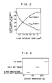
- Fig. 2 shows the relationship between an X-ray exposure dose and the composition of an Si wafer surface in Example 1.
- Fig. 3 shows a contact resistance measured in Example 1.
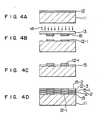
- Figs. 4A to 4D are cross sectional views showing steps for making a quantum wire in Example 5.
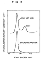
- Fig. 5 shows the results of photoelectron spectroscopy of Si surfaces achieved in Example 6.
- the X-ray or electron beam irradiation causes only electronic excitation on the surface atoms or the atoms composing the surface molecules, and the replacement of atom in lattice is so small as to be negligible as in conventional ion irradiation.
- a wafer material suffers little damage for the irradiation.
- the binding state of the surface atoms can be changed, whereby the reaction efficiency of the desorption reaction of specific atoms or molecules can be improved.
- the above radiation particle energy is an photon energy in the case of X-ray or an electron energy in the case of electron beam, and these energies are required to be over the ionization energy of the core electrons in order to cause the desorption.
- the present invention can be applied, for example, to the steps shown in the following Table 1.
- a native oxide film SiO, AlO, etc.
- the specific atom to be removed is an oxygen atom.
- the substrate is exposed to a light (X-rays or electron beams) having energy over the ionization energy of core electrons of atom(s) composing the surface of the substrate (solid sample) or oxygen to be removed, the removal of oxygen becomes possible based on the principle mentioned above.
- Table 1 typical values of ionization energy are shown.
- Such a technique for removing a specific atom exhibits its effectiveness when applied to regions such as gates, contact holes, capacitor forming portions, etc., of, e.g., semiconductor transistors, wherein good electroconductivity or insulation is required. Further, it is possible to selectively clean the surfaces of only these portions by exposing the surfaces to the light through a suitable mask.
- S sulfur
- adsorption layer formed for stabilizing the surface of GaAs substrate, a GaAlAs molecule layer in III-V group multi-layer structure, and an adsorption layer of a hydrocarbon which is a residue of a resist after a photolithographic step, and the like.
- FIGs. 1A to 1E A boron-doped (100) Si wafer 1 having a resistivity of 10 ⁇ -cm was prepared.
- the wafer was wet-washed with cleaning solutions 4 to remove organic materials 2 such as hydrocarbons, etc., and heavy metals 3 such as Cu, Ag, etc., which adhered to the wafer surface (Fig. 1A).
- Two kinds of cleaning solutions were used: One of which had a composition of NH4OH, H2O2 and H2O, and the other, a composition of HCl, H2O2 and H2O.
- the former is useful to remove organic materials, and the latter, metals.
- the Si wafer 1 When the washed Si wafer 1 was dried, the formation of a native oxide layer 6 occurred on its surface (Fig. 1B). Then, the Si wafer 1 was placed in an X-ray exposure chamber, and the chamber was evacuated to not more than 1 x 10 ⁇ 7 Pa. Thereafter, the surface of the Si wafer 1 was irradiated with X-ray 5 (Fig. 1C). Synchrotron radiation (electron acceleration energy: 2.5 GeV) was used as an X-ray source. Due to the reflection characteristics of an expansion mirror for synchrotron radiation beam and the transmissivity of a vacuum protection Be aperture of the synchrotron, the wavelength of the X-ray 5 for the irradiation to the sample Si wafer 1 was in the range of 0.5 to 1 nm.
- Synchrotron radiation electron acceleration energy: 2.5 GeV
- Fig. 2 is a graph showing the results.
- the atomic densities were determined on the basis of the intensity of surface Auger electrons (Si LVV and O KLL ).
- the graph shows, by irradiation with X-ray 5 having an energy intensity of not less than 1.2 J/cm2, that the O KLL became zero and that the Si wafer 1 had oxygen atoms selectively desorbed from the native oxide layer 6 on the surface and had a surface state of only the simple substance Si (Fig. 1D).
- Al was evaporated on the surface of the Si wafer 1 from which the native oxide layer 6 had been removed by the irradiation with the X-ray 5 having an energy intensity of 1.2 J/cm2, and then the evaporated Al was processed into a pattern having a 100 ⁇ m by 100 ⁇ m size (Fig. 1E).
- the Al pattern was used as an electrode to measure an Al/Si contact resistance. The measurement showed that the contact resistance could be reduced to about 50 ⁇ , about 1/5 of that in the case of no wash, and about 1/3 of that in the case of conventional wet wash.
- the reduction in the contact resistance is due to the effect produced by the removal of the native oxide layer 6 from the Si wafer 1 surface, i.e. due to the cleaning of the Si wafer 1 surface.
- the surface of an Si wafer prepared for the formation of an insulator for a capacitor was wet-washed in the same way as in Example 1.
- the Si wafer was dried and then placed in an X-ray exposure chamber.
- the chamber was evacuated to not more than 1 x 10 ⁇ 7 Pa.
- the si wafer as a sample was exposed to a reaction gas SF6, XeF2 or H2 (pressure 1 x 10 ⁇ 4 Pa) for 1 minute with cooling the wafer to -100°C, whereby the SF6 or XeF2 was adsorbed on the Si wafer surface.
- the surface on which SF6 was adsorbed caused shift of electrons, and the binding strength between an oxygen atom and Si atom on the surface was reduced.
- the chamber was re-evacuated and the Si wafer was irradiated with X-ray. Further, the procedure of adsorption-evacuation-irradiation was repeated, in which the total X-ray irradiation dose was 300 mJ/cm2 which was lower than that in Example 1, whereby a native oxide layer having a thickness of about 1.5 nm was removed.
- NH3 was introduced into the chamber to nitride the Si wafer surface (thickness 2 nm). Further, an Si3N4 film (thickness 5 nm) was formed by chemical vapor deposition, and an oxide film (thickness 1 nm) was then formed to produce a capacitor.
- a boron-doped Si (100) wafer was wet-washed in the same way as in Example 1, and then, placed in an electron beam exposure chamber.
- the chamber was evacuated to not more than 1 x 10 ⁇ 7 Pa, and the Si wafer surface was irradiated with electron beam.
- the acceleration energy of the electron beam for the irradiation was 2 KeV and the radiation dose thereof was 5 x 10 ⁇ 2 C/cm2.
- an Al electrode was formed under vacuum, and the contact resistance thereof was measured to show 60 ⁇ which corresponded to about 1/3 of that in the case of only wet wash.
- a boron-doped Si (100) wafer was wet-washed and dried in the same way as in Example 1. Then, the wafer was placed in a soft X-ray exposure chamber, and the chamber was evacuated to not more than 1 x 10 ⁇ 7 Pa.
- the X-ray irradiation method and irradiation conditions were the same as those in Example 1 except that an SF6 gas was introduced into the chamber during the X-ray irradiation so that the gas pressure was in the range of 1 to 10 Torr. Accordingly, a chemical reaction proceeded because of the Si surface excited by an X-ray excitation reaction and activated molecules produced by SF6 decomposition, whereby an oxide layer on the Si surface was selectively removed.
- FIG. 4A A method of making a two-dimensional quantum effect device (quantum wire) by co-using this invention and a molecular beam epitaxy is explained by reference to Figs. 4A to 4D.
- An AlAs monomolecular layer 12 was formed on a GaAs crystal wafer 11 according to molecular beam epitaxy (Fig. 4A). Then, the AlAs monomolecular layer 12 was irradiated with X-ray 14 through an X-ray mask 13 having an Au pattern 16 (Fig. 4B).
- the irradiation method and conditions for the X-ray 14 were the same as those in Example 1.
- the irradiation dose was 500 mJ/cm2.
- This Example describes the steps of cleaning the entire surface of an Si wafer without using any wet process such as acid solution treatment but by using synchrotron radiation as an excitation radiation source.
- an unwashed (100) Si wafer is placed in an X-ray exposure chamber, and the chamber is evacuated to not more than 1 x 10 ⁇ 5 Pa. Then, a oxygen gas is introduced into the chamber so that the pressure inside the chamber is in the range of 10 to 100 Torr.
- the Si wafer is irradiated with synchrotron radiation to generate chemically active atomic oxygen due to core electron excitation of oxygen molecules.
- the atomic oxygen reacts with hydrocarbons adsorbed on the Si surface to form carbon dioxide (CO2) and water (H2O), which are desorbed from the surface.
- CO2 carbon dioxide
- H2O water
- Fig. 5 shows the results of photoelectron spectroscopy of an Si wafer surface treated according to this Example and an Si wafer surface subjected to only wet wash treatment as in Example 1.
- This Example has a feature that a clean Si wafer surface can be stably obtained since the removal of adsorbed hydrocarbons and oxides can be carried out in vacuum.
Landscapes
- Cleaning Or Drying Semiconductors (AREA)
- Drying Of Semiconductors (AREA)
- Analysing Materials By The Use Of Radiation (AREA)
Applications Claiming Priority (2)
| Application Number | Priority Date | Filing Date | Title |
|---|---|---|---|
| JP136017/89 | 1989-05-31 | ||
| JP1136017A JPH033328A (ja) | 1989-05-31 | 1989-05-31 | 固体試料表面の改質方法 |
Publications (2)
| Publication Number | Publication Date |
|---|---|
| EP0400651A2 true EP0400651A2 (fr) | 1990-12-05 |
| EP0400651A3 EP0400651A3 (fr) | 1991-12-11 |
Family
ID=15165238
Family Applications (1)
| Application Number | Title | Priority Date | Filing Date |
|---|---|---|---|
| EP19900110374 Withdrawn EP0400651A3 (fr) | 1989-05-31 | 1990-05-31 | Procédé de modification sur la surface d'un corps solide |
Country Status (2)
| Country | Link |
|---|---|
| EP (1) | EP0400651A3 (fr) |
| JP (1) | JPH033328A (fr) |
Cited By (5)
| Publication number | Priority date | Publication date | Assignee | Title |
|---|---|---|---|---|
| EP0562848A3 (en) * | 1992-03-27 | 1996-01-17 | Hitachi Ltd | Surface treating method |
| EP0690485A3 (fr) * | 1994-06-29 | 1997-04-16 | At & T Corp | Traitement de surface pour substrates en silicium |
| EP0735428A3 (fr) * | 1995-03-31 | 1998-06-10 | Shimadzu Corporation | Méthode pour réaliser des motifs fins et appareil à motifs fins |
| US6554950B2 (en) | 2001-01-16 | 2003-04-29 | Applied Materials, Inc. | Method and apparatus for removal of surface contaminants from substrates in vacuum applications |
| WO2009152329A3 (fr) * | 2008-06-14 | 2010-03-11 | Applied Materials, Inc. | Procédé de traitement de surface de substrats semi-conducteurs |
Family Cites Families (2)
| Publication number | Priority date | Publication date | Assignee | Title |
|---|---|---|---|---|
| US4590091A (en) * | 1984-12-17 | 1986-05-20 | Hughes Aircraft Company | Photochemical process for substrate surface preparation |
| GB8806800D0 (en) * | 1988-03-22 | 1988-04-20 | British Telecomm | Etching methods |
-
1989
- 1989-05-31 JP JP1136017A patent/JPH033328A/ja active Pending
-
1990
- 1990-05-31 EP EP19900110374 patent/EP0400651A3/fr not_active Withdrawn
Cited By (8)
| Publication number | Priority date | Publication date | Assignee | Title |
|---|---|---|---|---|
| EP0562848A3 (en) * | 1992-03-27 | 1996-01-17 | Hitachi Ltd | Surface treating method |
| EP0690485A3 (fr) * | 1994-06-29 | 1997-04-16 | At & T Corp | Traitement de surface pour substrates en silicium |
| EP0735428A3 (fr) * | 1995-03-31 | 1998-06-10 | Shimadzu Corporation | Méthode pour réaliser des motifs fins et appareil à motifs fins |
| US6554950B2 (en) | 2001-01-16 | 2003-04-29 | Applied Materials, Inc. | Method and apparatus for removal of surface contaminants from substrates in vacuum applications |
| WO2002063661A3 (fr) * | 2001-01-16 | 2003-12-18 | Applied Materials Inc | Procede et appareil permettant l'elimination de contaminants de surface de substrats dans des applications a vide |
| US7067399B2 (en) | 2001-01-16 | 2006-06-27 | Applied Materials, Inc. | Method and apparatus for removal of surface contaminants from substrates in vacuum applications |
| WO2009152329A3 (fr) * | 2008-06-14 | 2010-03-11 | Applied Materials, Inc. | Procédé de traitement de surface de substrats semi-conducteurs |
| US7838431B2 (en) | 2008-06-14 | 2010-11-23 | Applied Materials, Inc. | Method for surface treatment of semiconductor substrates |
Also Published As
| Publication number | Publication date |
|---|---|
| JPH033328A (ja) | 1991-01-09 |
| EP0400651A3 (fr) | 1991-12-11 |
Similar Documents
| Publication | Publication Date | Title |
|---|---|---|
| JP3086719B2 (ja) | 表面処理方法 | |
| US5030319A (en) | Method of oxide etching with condensed plasma reaction product | |
| KR100391840B1 (ko) | 반도체기판표면상의절연막형성방법및그형성장치 | |
| EP0191143B1 (fr) | Procédé photochimique pour préparer la surface d'un substrat | |
| US5332444A (en) | Gas phase cleaning agents for removing metal containing contaminants from integrated circuit assemblies and a process for using the same | |
| Green et al. | Do we need a new methodology for GaAs passivation? | |
| EP1038307A1 (fr) | Modification de surface des semiconducteurs par rayonnement electromagnetique | |
| Akazawa et al. | Photostimulated evaporation of SiO2 and Si3N4 films by synchrotron radiation and its application for low‐temperature cleaning of Si surfaces | |
| Fukuda et al. | Electron‐cyclotron‐resonance plasma‐enhanced chemical vapor deposition of epitaxial Si without substrate heating by ultraclean processing | |
| Gamo et al. | Ion beam assisted etching and deposition | |
| JPH033328A (ja) | 固体試料表面の改質方法 | |
| JP2694625B2 (ja) | 化合物半導体基体のエッチング方法および製造方法 | |
| Sugino et al. | Schottky junctions on phosphidized GaAs surfaces | |
| JP2922149B2 (ja) | 微細加工方法 | |
| JP2699928B2 (ja) | 化合物半導体基板の前処理方法 | |
| JP3198302B2 (ja) | 微細構造パターンの形成方法 | |
| Ogawa et al. | Low‐temperature synchrotron‐radiation‐excited etching of silicon dioxide with sulfur hexafluoride adsorption | |
| JP2737613B2 (ja) | 微細パターンの形成方法 | |
| JP2985321B2 (ja) | マスクパタ−ン形成方法 | |
| JPH06291095A (ja) | パターン形成方法 | |
| Mazur et al. | UPS study of KOH layers on Si (100) surface | |
| JP2709175B2 (ja) | エッチングパターンの形成方法 | |
| Takado et al. | New in situ electron beam patterning process for GaAs using an electron‐cyclotron‐resonance plasma‐oxidized mask and Cl2 gas etching | |
| JPH065559A (ja) | オゾンプラズマ処理 | |
| Gamo | Ion beam microfabrication |
Legal Events
| Date | Code | Title | Description |
|---|---|---|---|
| PUAI | Public reference made under article 153(3) epc to a published international application that has entered the european phase |
Free format text: ORIGINAL CODE: 0009012 |
|
| 17P | Request for examination filed |
Effective date: 19900531 |
|
| AK | Designated contracting states |
Kind code of ref document: A2 Designated state(s): DE FR GB |
|
| RHK1 | Main classification (correction) |
Ipc: H01L 21/263 |
|
| PUAL | Search report despatched |
Free format text: ORIGINAL CODE: 0009013 |
|
| AK | Designated contracting states |
Kind code of ref document: A3 Designated state(s): DE FR GB |
|
| 17Q | First examination report despatched |
Effective date: 19920707 |
|
| STAA | Information on the status of an ep patent application or granted ep patent |
Free format text: STATUS: THE APPLICATION HAS BEEN WITHDRAWN |
|
| 18W | Application withdrawn |
Withdrawal date: 19941004 |