EP0400748A2 - Method and device for the arithmetical calculation of two-dimensional transforms - Google Patents
Method and device for the arithmetical calculation of two-dimensional transforms Download PDFInfo
- Publication number
- EP0400748A2 EP0400748A2 EP90201351A EP90201351A EP0400748A2 EP 0400748 A2 EP0400748 A2 EP 0400748A2 EP 90201351 A EP90201351 A EP 90201351A EP 90201351 A EP90201351 A EP 90201351A EP 0400748 A2 EP0400748 A2 EP 0400748A2
- Authority
- EP
- European Patent Office
- Prior art keywords
- data
- multiplication
- multiplier
- transform
- transformed
- Prior art date
- Legal status (The legal status is an assumption and is not a legal conclusion. Google has not performed a legal analysis and makes no representation as to the accuracy of the status listed.)
- Granted
Links
Images
Classifications
-
- G—PHYSICS
- G06—COMPUTING OR CALCULATING; COUNTING
- G06F—ELECTRIC DIGITAL DATA PROCESSING
- G06F17/00—Digital computing or data processing equipment or methods, specially adapted for specific functions
- G06F17/10—Complex mathematical operations
- G06F17/14—Fourier, Walsh or analogous domain transformations, e.g. Laplace, Hilbert, Karhunen-Loeve, transforms
-
- G—PHYSICS
- G06—COMPUTING OR CALCULATING; COUNTING
- G06F—ELECTRIC DIGITAL DATA PROCESSING
- G06F7/00—Methods or arrangements for processing data by operating upon the order or content of the data handled
-
- G—PHYSICS
- G06—COMPUTING OR CALCULATING; COUNTING
- G06F—ELECTRIC DIGITAL DATA PROCESSING
- G06F17/00—Digital computing or data processing equipment or methods, specially adapted for specific functions
- G06F17/10—Complex mathematical operations
- G06F17/16—Matrix or vector computation, e.g. matrix-matrix or matrix-vector multiplication, matrix factorization
Definitions
- the present invention relates to a method and a device for the arithmetical calculation of two-dimensional transforms.
- This coding technique ensures the decorrelation of the original signal and executes its energy compacting. Such an operation reduces signal redundancy, allowing the minimization of the quantity of information necessary for coding.
- the devices available on the market are designed to support only one particular type of unitary transform.
- the object of the present invention is to design a method and a device for the arithmetical calculation of any two-dimensional unitary transform which allows operations in real time with a high speed of calculation and which has a particularly simple architecture.
- such object is attained by means of a method characterized in that it comprises two time steps of multiplication and accumulation, a first step being assigned to the product of the data and of the coefficient matrices and a second step being assigned to the subsequent product by the transposed coefficient matrix.
- the data to be transformed and the corresponding coefficients be supplied to the first multiplication step in a time succession, possibly after being stored in a suitable memory.
- a device for the attainment of the above method characterized in that it comprises two multipliers with their corresponding accumulator, a first multiplier with its corresponding accumulator executing the multiplication of the transform coefficient matrix by the input data matrix, a second multiplier with its corresponding accumulator receiving at input the result of this first multiplication and multiplying it by the transposed transform coefficient matrix.
- the device in addition, still according to the invention provision is made for the device to include a RAM-type memory for storing the data to be transformed and the transform coefficients together with a multiplexer which receives said data first from input and then from storage, and arranges them in a time succession for supply.
- the device essentially comprises two multipliers 31, 32, in series having 8x8 and 12x8 bits respectively, which both work in module and token.
- a first accumulator indicated in the figure with 33, which has the task of accumulating the first matrix product (data matrix by coefficient matrix).
- said accumulator 33 contains in a way known in itself and not shown in the drawing an adder/subtractor (piloted by the token bit and operating on the module coming from the multiplier 31) for the accumulation of the partial sums necessary for the first matrix operation, a second adder/subtractor for the reconversion to module and token, six registers for the reconversion of the data flow and two multiplexers necessary for accumulator reset.
- a dual-gate RAM 34 with the possibility of partially writing each word's content is in a position of memorizing the coefficient matrix and that of the data; its dimensions (18 bits for 64 words) makes it possible to have both the data and the coefficients available with just one address.
- Programning of RAM 34 is executed by varying the content of the part of RAM 34 containing the transform coefficients. The contents of the part of RAM 34 containing the data is varied each time a new matrix to be transformed arrives.
- the input lines to RAM 34 come from three registers, of which the registers indicated with 35 and 36 load the coefficients and the matrix data, respectively, transforming them from the twos complement notation to that of module and token. Said input data and coefficients are supplied to registers 35, 36 along input buses 40, 41.
- the third register indicated with 37 is controlled by a suitable microprocessor with which it communicates by means of connections 42, 43 and contains a programmable logic array (PLA) to generate the control signals for controlling the device's logic operation, a random logic supporting the PLA and a 9-bit counter to generate the RAM 34 addresses.
- PDA programmable logic array
- a set of three connections depart from RAM 34, two of which are used to supply the coefficients of the transposed matrix to the multiplier 32 through a shift register 38 and to supply the data to be transformed to a two-to-one multiplexer register indicated with 39 with which it is possible to route on the first multiplier 31 the data coming from register 36 (for the first 64 clock cycles) or from RAM 34 (subsequent clock cycles), respectively.
- the third connection allows the RAM to supply the transform coefficients to multiplier 31.
- An accumulator 30 allows the accumulation of a second matrix product (first matrix product by transposed matrix coefficient) giving a twos complement output. Inside it, in a way known in itself and not shown in the drawing, there are just one adder/subtractor (driven by the token bit and operating on the module coming from the output of accumulator 33), a multiplexer for reset, nine registers for the synchronization of the data flow.
- the output line 44 departs from said accumulator.
- the device occupies in succession a group of three states, wait, load, calculation, the transition between which is regulated by a group of commands by means of which the device executes the transform operation.
Landscapes
- Engineering & Computer Science (AREA)
- Physics & Mathematics (AREA)
- General Physics & Mathematics (AREA)
- Mathematical Physics (AREA)
- Theoretical Computer Science (AREA)
- Computational Mathematics (AREA)
- Mathematical Analysis (AREA)
- Mathematical Optimization (AREA)
- Pure & Applied Mathematics (AREA)
- Data Mining & Analysis (AREA)
- General Engineering & Computer Science (AREA)
- Algebra (AREA)
- Databases & Information Systems (AREA)
- Software Systems (AREA)
- Computing Systems (AREA)
- Complex Calculations (AREA)
Abstract
Description
- The present invention relates to a method and a device for the arithmetical calculation of two-dimensional transforms.
- In many fields of technology there exists the need of executing coding for transmission and recording of numerical signals by means of two-dimensional transforms.
- This coding technique ensures the decorrelation of the original signal and executes its energy compacting. Such an operation reduces signal redundancy, allowing the minimization of the quantity of information necessary for coding.
- For any type of signal (voice, video, data), the optimum transform in terms of decorrelation capacity is the Karhunen-Loewe transform; unfortunately the computational complexity of the algorithm, and as a consequence the length of calculation time required, makes it difficult to use it within the ambit of industrial applications wherein it is required that the signal transform operation be carried out in real time (coding of images in motion).
- In practice different types of sub-optimum unitary transforms are used: discrete Fourier transform, discrete sine transform, discrete cosine transform, Hadamard transform, slant transform.
- The choice of a particular type of unitary transform is dictated by the statistical characteristics of the signal to be coded.
- The devices available on the market are designed to support only one particular type of unitary transform.
- The object of the present invention is to design a method and a device for the arithmetical calculation of any two-dimensional unitary transform which allows operations in real time with a high speed of calculation and which has a particularly simple architecture.
- According to the invention such object is attained by means of a method characterized in that it comprises two time steps of multiplication and accumulation, a first step being assigned to the product of the data and of the coefficient matrices and a second step being assigned to the subsequent product by the transposed coefficient matrix.
- According to the invention it is also provided that the data to be transformed and the corresponding coefficients be supplied to the first multiplication step in a time succession, possibly after being stored in a suitable memory.
- It has been possible to note that in this way a good compromise has been obtained between the occupation of silicon area and the speed of calculation.
- According to the invention there is further accomplished a device for the attainment of the above method, characterized in that it comprises two multipliers with their corresponding accumulator, a first multiplier with its corresponding accumulator executing the multiplication of the transform coefficient matrix by the input data matrix, a second multiplier with its corresponding accumulator receiving at input the result of this first multiplication and multiplying it by the transposed transform coefficient matrix.
- In addition, still according to the invention provision is made for the device to include a RAM-type memory for storing the data to be transformed and the transform coefficients together with a multiplexer which receives said data first from input and then from storage, and arranges them in a time succession for supply.
- With the introduction of the multiplexer it has been possible to attain considerable speeds of calculation, while the use of the RAM memory has allowed extreme operational flexibility allowing, as the case may be, to select the type of the transform most suitable for the particular problem to be solved. The transform's arithmetical calculation thus becomes programmable simply by varying the transform coefficients stored in the RAM.
- These and other features of the present invention shall be made evident by the following detailed description of an embodiment illustrated as a non-limiting example in the enclosed drawings, wherein:
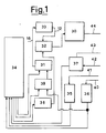
- Fig. 1 shows the architecture of a device according to the invention;
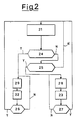
- Fig. 2 shows the logic operating sequence of the device in compliance with the method according to the invention.
- Considering first Fig. 1, the device according to the invention essentially comprises two
multipliers multiplier 31 there is arranged a first accumulator, indicated in the figure with 33, which has the task of accumulating the first matrix product (data matrix by coefficient matrix). Internally saidaccumulator 33 contains in a way known in itself and not shown in the drawing an adder/subtractor (piloted by the token bit and operating on the module coming from the multiplier 31) for the accumulation of the partial sums necessary for the first matrix operation, a second adder/subtractor for the reconversion to module and token, six registers for the reconversion of the data flow and two multiplexers necessary for accumulator reset. - A
dual-gate RAM 34 with the possibility of partially writing each word's content is in a position of memorizing the coefficient matrix and that of the data; its dimensions (18 bits for 64 words) makes it possible to have both the data and the coefficients available with just one address. Programning ofRAM 34 is executed by varying the content of the part ofRAM 34 containing the transform coefficients. The contents of the part ofRAM 34 containing the data is varied each time a new matrix to be transformed arrives. - The input lines to
RAM 34 come from three registers, of which the registers indicated with 35 and 36 load the coefficients and the matrix data, respectively, transforming them from the twos complement notation to that of module and token. Said input data and coefficients are supplied to registers 35, 36 alonginput buses connections RAM 34 addresses. - A set of three connections depart from
RAM 34, two of which are used to supply the coefficients of the transposed matrix to themultiplier 32 through ashift register 38 and to supply the data to be transformed to a two-to-one multiplexer register indicated with 39 with which it is possible to route on thefirst multiplier 31 the data coming from register 36 (for the first 64 clock cycles) or from RAM 34 (subsequent clock cycles), respectively. The third connection allows the RAM to supply the transform coefficients to multiplier 31. - An
accumulator 30 allows the accumulation of a second matrix product (first matrix product by transposed matrix coefficient) giving a twos complement output. Inside it, in a way known in itself and not shown in the drawing, there are just one adder/subtractor (driven by the token bit and operating on the module coming from the output of accumulator 33), a multiplexer for reset, nine registers for the synchronization of the data flow. - The
output line 44 departs from said accumulator. - Due to the effect of the described structure, during its operation the device occupies in succession a group of three states, wait, load, calculation, the transition between which is regulated by a group of commands by means of which the device executes the transform operation.
- The flow chart related to this group of commands is represented in Fig. 2.
- In it there are present three
functional registers loading 24,calculation 25, end ofcoefficient loading operation 26, end ofcalculation operation 27, respectively. - There are also two registers, indicated with 28, 29, to signal that the
coefficient loading step 22 or thecalculation step 23 are under way, respectively. A suitable operational flag is placed on one during such steps. - The letters Y and N indicate positive or negative replies at the output from
registers - More precisely, from the waiting step,
functional register 21, inside which an operational flag is forced to 0, we go to the step of loading request, register 24, from which in case of a positive reply Y we go to the coefficient loading step,functional register 22, having previously signalled the start of this step by giving a value 1 to the operational flag inside register 29. Theinput register 35 of Fig. 1 then loads the transform coefficient intoRAM 34. - In case of a negative reply at the output of the
loading polling register 24 we go to thecalculation polling register 25. - From this register, in case of a negative reply we return to the waiting step,
functional register 21; in case of a positive reply, on the other hand, we go tofunctional register 23, corresponding to the calculation step, having previously signalled the start of this step by giving a value 1 to the operational flag inside register 28. There is thus started the operation of transform calculation using for the first 64 clock cycles the data loaded by theinput register 36 of Fig. 1 and for the following the matrix data loaded in the meantime by thesame register 36 intoRAM 34. The calculation is executed by the twomultipliers corresponding accumulators - From the end of
operation polling registers functional register 21, while in the case of a negative reply we continue the current operation returning throughregisters functional registers - It should be noted that the calculation of the two-dimensional transform is programmable by varying only that part of RAM (34) which contains the matrix of the transform coefficients.
Claims (8)
Applications Claiming Priority (2)
| Application Number | Priority Date | Filing Date | Title |
|---|---|---|---|
| IT2074489 | 1989-06-02 | ||
| IT8920744A IT1235263B (en) | 1989-06-02 | 1989-06-02 | METHOD AND DEVICE FOR THE ARITHMETIC CALCULATION OF TWO-DIMENSIONAL PROCESSES. |
Publications (3)
| Publication Number | Publication Date |
|---|---|
| EP0400748A2 true EP0400748A2 (en) | 1990-12-05 |
| EP0400748A3 EP0400748A3 (en) | 1991-10-23 |
| EP0400748B1 EP0400748B1 (en) | 1997-08-20 |
Family
ID=11171421
Family Applications (1)
| Application Number | Title | Priority Date | Filing Date |
|---|---|---|---|
| EP90201351A Expired - Lifetime EP0400748B1 (en) | 1989-06-02 | 1990-05-29 | Method and device for the arithmetical calculation of two-dimensional transforms |
Country Status (8)
| Country | Link |
|---|---|
| US (1) | US5140542A (en) |
| EP (1) | EP0400748B1 (en) |
| JP (1) | JPH0387974A (en) |
| KR (1) | KR910001532A (en) |
| BR (1) | BR9002615A (en) |
| DE (1) | DE69031293T2 (en) |
| IT (1) | IT1235263B (en) |
| PL (1) | PL163731B1 (en) |
Families Citing this family (2)
| Publication number | Priority date | Publication date | Assignee | Title |
|---|---|---|---|---|
| US5345408A (en) * | 1993-04-19 | 1994-09-06 | Gi Corporation | Inverse discrete cosine transform processor |
| US12610082B2 (en) * | 2021-12-06 | 2026-04-21 | Intel Corporation | Unrestricted intra content to improve video quality of real-time encoding |
Family Cites Families (8)
| Publication number | Priority date | Publication date | Assignee | Title |
|---|---|---|---|---|
| US4554629A (en) * | 1983-02-22 | 1985-11-19 | Smith Jr Winthrop W | Programmable transform processor |
| FR2582424B1 (en) * | 1985-05-22 | 1989-06-30 | Guichard Jacques | CIRCUIT OF FAST CALCULATION OF THE TRANSFORMED IN COSINUS, DIRECT OR REVERSE, OF A DISCRETE SIGNAL |
| FR2599872B1 (en) * | 1986-06-06 | 1988-07-29 | Thomson Csf | DEVICES FOR CALCULATING MONO-DIMENSIONAL COSINE TRANSFORMS, AND CODING DEVICE AND IMAGE DECODING DEVICE COMPRISING SUCH COMPUTING DEVICES |
| US4829465A (en) * | 1986-06-19 | 1989-05-09 | American Telephone And Telegraph Company, At&T Bell Laboratories | High speed cosine transform |
| JPS63154205A (en) * | 1986-12-17 | 1988-06-27 | Kawasaki Steel Corp | Rolling method by mandrel mill for seamless austenitic stainless steel tube |
| NL8700843A (en) * | 1987-04-10 | 1988-11-01 | Philips Nv | TELEVISION TRANSFER SYSTEM WITH TRANSFORM CODING. |
| DE3773192D1 (en) * | 1987-05-02 | 1991-10-24 | Ant Nachrichtentech | METHOD FOR TWO-DIMENSIONAL SPECTRAL INFORMATION. |
| ES2011327A6 (en) * | 1988-03-30 | 1990-01-01 | Alcatel Standard Electrica | Method and device for obtaining in real time the two-dimensional discrete cosine transform. |
-
1989
- 1989-06-02 IT IT8920744A patent/IT1235263B/en active
-
1990
- 1990-05-29 EP EP90201351A patent/EP0400748B1/en not_active Expired - Lifetime
- 1990-05-29 DE DE69031293T patent/DE69031293T2/en not_active Expired - Fee Related
- 1990-06-01 BR BR909002615A patent/BR9002615A/en not_active IP Right Cessation
- 1990-06-01 JP JP2141719A patent/JPH0387974A/en active Pending
- 1990-06-01 PL PL90285432A patent/PL163731B1/en unknown
- 1990-06-01 US US07/531,719 patent/US5140542A/en not_active Expired - Lifetime
- 1990-06-02 KR KR1019900008218A patent/KR910001532A/en not_active Withdrawn
Also Published As
| Publication number | Publication date |
|---|---|
| PL163731B1 (en) | 1994-04-29 |
| US5140542A (en) | 1992-08-18 |
| IT1235263B (en) | 1992-06-26 |
| BR9002615A (en) | 1991-08-20 |
| KR910001532A (en) | 1991-01-31 |
| EP0400748B1 (en) | 1997-08-20 |
| JPH0387974A (en) | 1991-04-12 |
| EP0400748A3 (en) | 1991-10-23 |
| IT8920744A0 (en) | 1989-06-02 |
| DE69031293T2 (en) | 1998-01-15 |
| DE69031293D1 (en) | 1997-09-25 |
Similar Documents
| Publication | Publication Date | Title |
|---|---|---|
| US4791598A (en) | Two-dimensional discrete cosine transform processor | |
| US5202847A (en) | Digital signal processing | |
| EP0068358B1 (en) | Apparatus for parallel processing of local image data | |
| US5331585A (en) | Orthogonal transformation processor for compressing information | |
| US4725973A (en) | Vector processor | |
| US12412081B2 (en) | Method for permuting dimensions of a multi-dimensional tensor | |
| US4970674A (en) | Programmable windowing FFT device with reduced memory requirements | |
| US6282555B1 (en) | Orthogonal transform processor | |
| US11669733B2 (en) | Processing unit and method for computing a convolution using a hardware-implemented spiral algorithm | |
| EP0997828A2 (en) | Signal processing distributed arithmetic architecture | |
| KR880013401A (en) | I-Dimensional Image Converter | |
| EP0400748A2 (en) | Method and device for the arithmetical calculation of two-dimensional transforms | |
| US5029079A (en) | Apparatus and method for flexible control of digital signal processing devices | |
| US5434808A (en) | Highly parallel discrete cosine transform engine | |
| US5359549A (en) | Orthogonal transformation processor for compressing information | |
| AU611002B2 (en) | Discrete cosine transform | |
| GB2306716A (en) | Performing bit-serial matrix transposition operations | |
| US6023719A (en) | Signal processor and method for fast Fourier transformation | |
| JP2002269067A (en) | Matrix arithmetic unit | |
| Waltz | SKIPSM implementations: morphology and much, much more | |
| US5327367A (en) | Computer system with vector functional unit for fast fourier transform | |
| US6199143B1 (en) | Computing system with fast data transfer of CPU state related information | |
| JPH1063647A (en) | Matrix arithmetic unit | |
| EP0500383A2 (en) | Data processing system | |
| US5245562A (en) | Accumulating arithmetic memory integrated circuit |
Legal Events
| Date | Code | Title | Description |
|---|---|---|---|
| PUAI | Public reference made under article 153(3) epc to a published international application that has entered the european phase |
Free format text: ORIGINAL CODE: 0009012 |
|
| AK | Designated contracting states |
Kind code of ref document: A2 Designated state(s): DE FR GB NL SE |
|
| PUAL | Search report despatched |
Free format text: ORIGINAL CODE: 0009013 |
|
| AK | Designated contracting states |
Kind code of ref document: A3 Designated state(s): DE FR GB NL SE |
|
| 17P | Request for examination filed |
Effective date: 19920325 |
|
| 17Q | First examination report despatched |
Effective date: 19951012 |
|
| GRAG | Despatch of communication of intention to grant |
Free format text: ORIGINAL CODE: EPIDOS AGRA |
|
| GRAH | Despatch of communication of intention to grant a patent |
Free format text: ORIGINAL CODE: EPIDOS IGRA |
|
| RHK1 | Main classification (correction) |
Ipc: G06F 17/16 |
|
| GRAH | Despatch of communication of intention to grant a patent |
Free format text: ORIGINAL CODE: EPIDOS IGRA |
|
| GRAA | (expected) grant |
Free format text: ORIGINAL CODE: 0009210 |
|
| AK | Designated contracting states |
Kind code of ref document: B1 Designated state(s): DE FR GB NL SE |
|
| PG25 | Lapsed in a contracting state [announced via postgrant information from national office to epo] |
Ref country code: NL Free format text: LAPSE BECAUSE OF FAILURE TO SUBMIT A TRANSLATION OF THE DESCRIPTION OR TO PAY THE FEE WITHIN THE PRESCRIBED TIME-LIMIT Effective date: 19970820 |
|
| REF | Corresponds to: |
Ref document number: 69031293 Country of ref document: DE Date of ref document: 19970925 |
|
| PG25 | Lapsed in a contracting state [announced via postgrant information from national office to epo] |
Ref country code: SE Effective date: 19971120 |
|
| ET | Fr: translation filed | ||
| NLV1 | Nl: lapsed or annulled due to failure to fulfill the requirements of art. 29p and 29m of the patents act | ||
| PLBE | No opposition filed within time limit |
Free format text: ORIGINAL CODE: 0009261 |
|
| STAA | Information on the status of an ep patent application or granted ep patent |
Free format text: STATUS: NO OPPOSITION FILED WITHIN TIME LIMIT |
|
| 26N | No opposition filed | ||
| REG | Reference to a national code |
Ref country code: FR Ref legal event code: D6 |
|
| REG | Reference to a national code |
Ref country code: GB Ref legal event code: IF02 |
|
| PGFP | Annual fee paid to national office [announced via postgrant information from national office to epo] |
Ref country code: FR Payment date: 20020508 Year of fee payment: 13 |
|
| PGFP | Annual fee paid to national office [announced via postgrant information from national office to epo] |
Ref country code: GB Payment date: 20020529 Year of fee payment: 13 |
|
| PGFP | Annual fee paid to national office [announced via postgrant information from national office to epo] |
Ref country code: DE Payment date: 20020610 Year of fee payment: 13 |
|
| PG25 | Lapsed in a contracting state [announced via postgrant information from national office to epo] |
Ref country code: GB Free format text: LAPSE BECAUSE OF NON-PAYMENT OF DUE FEES Effective date: 20030529 |
|
| PG25 | Lapsed in a contracting state [announced via postgrant information from national office to epo] |
Ref country code: DE Free format text: LAPSE BECAUSE OF NON-PAYMENT OF DUE FEES Effective date: 20031202 |
|
| GBPC | Gb: european patent ceased through non-payment of renewal fee |
Effective date: 20030529 |
|
| PG25 | Lapsed in a contracting state [announced via postgrant information from national office to epo] |
Ref country code: FR Free format text: LAPSE BECAUSE OF NON-PAYMENT OF DUE FEES Effective date: 20040130 |
|
| REG | Reference to a national code |
Ref country code: FR Ref legal event code: ST |