EP0400854A2 - Procédé et dispositif pour le centrage de données - Google Patents
Procédé et dispositif pour le centrage de données Download PDFInfo
- Publication number
- EP0400854A2 EP0400854A2 EP90305478A EP90305478A EP0400854A2 EP 0400854 A2 EP0400854 A2 EP 0400854A2 EP 90305478 A EP90305478 A EP 90305478A EP 90305478 A EP90305478 A EP 90305478A EP 0400854 A2 EP0400854 A2 EP 0400854A2
- Authority
- EP
- European Patent Office
- Prior art keywords
- data
- error
- detection
- carrier
- compensate
- Prior art date
- Legal status (The legal status is an assumption and is not a legal conclusion. Google has not performed a legal analysis and makes no representation as to the accuracy of the status listed.)
- Withdrawn
Links
- 238000000034 method Methods 0.000 title claims abstract description 36
- 238000001514 detection method Methods 0.000 claims abstract description 60
- 230000008569 process Effects 0.000 claims abstract description 14
- 230000003321 amplification Effects 0.000 claims abstract description 12
- 238000003199 nucleic acid amplification method Methods 0.000 claims abstract description 12
- 238000006243 chemical reaction Methods 0.000 claims abstract description 6
- 238000010586 diagram Methods 0.000 description 6
- 230000005540 biological transmission Effects 0.000 description 5
- 230000008859 change Effects 0.000 description 3
- 239000003990 capacitor Substances 0.000 description 2
- 230000009977 dual effect Effects 0.000 description 2
- 230000001052 transient effect Effects 0.000 description 2
- 230000006978 adaptation Effects 0.000 description 1
- 230000008878 coupling Effects 0.000 description 1
- 238000010168 coupling process Methods 0.000 description 1
- 238000005859 coupling reaction Methods 0.000 description 1
- 230000004069 differentiation Effects 0.000 description 1
- 230000000694 effects Effects 0.000 description 1
- 230000007774 longterm Effects 0.000 description 1
- 238000012986 modification Methods 0.000 description 1
- 230000004048 modification Effects 0.000 description 1
Images
Classifications
-
- H—ELECTRICITY
- H04—ELECTRIC COMMUNICATION TECHNIQUE
- H04L—TRANSMISSION OF DIGITAL INFORMATION, e.g. TELEGRAPHIC COMMUNICATION
- H04L25/00—Baseband systems
- H04L25/02—Details ; arrangements for supplying electrical power along data transmission lines
- H04L25/06—DC level restoring means; Bias distortion correction ; Decision circuits providing symbol by symbol detection
-
- H—ELECTRICITY
- H04—ELECTRIC COMMUNICATION TECHNIQUE
- H04L—TRANSMISSION OF DIGITAL INFORMATION, e.g. TELEGRAPHIC COMMUNICATION
- H04L25/00—Baseband systems
- H04L25/02—Details ; arrangements for supplying electrical power along data transmission lines
- H04L25/06—DC level restoring means; Bias distortion correction ; Decision circuits providing symbol by symbol detection
- H04L25/061—DC level restoring means; Bias distortion correction ; Decision circuits providing symbol by symbol detection providing hard decisions only; arrangements for tracking or suppressing unwanted low frequency components, e.g. removal of DC offset
- H04L25/062—Setting decision thresholds using feedforward techniques only
-
- H—ELECTRICITY
- H04—ELECTRIC COMMUNICATION TECHNIQUE
- H04L—TRANSMISSION OF DIGITAL INFORMATION, e.g. TELEGRAPHIC COMMUNICATION
- H04L25/00—Baseband systems
- H04L25/02—Details ; arrangements for supplying electrical power along data transmission lines
- H04L25/06—DC level restoring means; Bias distortion correction ; Decision circuits providing symbol by symbol detection
- H04L25/061—DC level restoring means; Bias distortion correction ; Decision circuits providing symbol by symbol detection providing hard decisions only; arrangements for tracking or suppressing unwanted low frequency components, e.g. removal of DC offset
- H04L25/066—Multilevel decisions, not including self-organising maps
-
- H—ELECTRICITY
- H04—ELECTRIC COMMUNICATION TECHNIQUE
- H04L—TRANSMISSION OF DIGITAL INFORMATION, e.g. TELEGRAPHIC COMMUNICATION
- H04L27/00—Modulated-carrier systems
- H04L27/10—Frequency-modulated carrier systems, i.e. using frequency-shift keying
- H04L27/14—Demodulator circuits; Receiver circuits
- H04L27/142—Compensating direct current components occurring during the demodulation and which are caused by mistuning
Definitions
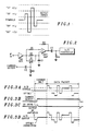
- the amount of gain is determined by the ratio of R2 divided by R1 .
- This ratio can be any value within the "raw" gain capability of the DIFF AMP employed, at the data rate of interest.
- the voltage component caused by frequency offset of the carrier which is now the same on both inputs to the DIFF AMP , has become a "common mode” component which is subject to the same gain, but since it is the same on both inputs, results in no "difference" to amplify. This entire process is repeated upon the loss of carrier and the arrival of another packet.
Landscapes
- Engineering & Computer Science (AREA)
- Computer Networks & Wireless Communication (AREA)
- Signal Processing (AREA)
- Power Engineering (AREA)
- Digital Transmission Methods That Use Modulated Carrier Waves (AREA)
- Dc Digital Transmission (AREA)
- Logic Circuits (AREA)
- Analogue/Digital Conversion (AREA)
Applications Claiming Priority (2)
| Application Number | Priority Date | Filing Date | Title |
|---|---|---|---|
| US358295 | 1989-05-26 | ||
| US07/358,295 US5148449A (en) | 1989-05-26 | 1989-05-26 | Centering multi-level data |
Publications (2)
| Publication Number | Publication Date |
|---|---|
| EP0400854A2 true EP0400854A2 (fr) | 1990-12-05 |
| EP0400854A3 EP0400854A3 (fr) | 1992-04-08 |
Family
ID=23409099
Family Applications (1)
| Application Number | Title | Priority Date | Filing Date |
|---|---|---|---|
| EP19900305478 Withdrawn EP0400854A3 (fr) | 1989-05-26 | 1990-05-21 | Procédé et dispositif pour le centrage de données |
Country Status (10)
| Country | Link |
|---|---|
| US (1) | US5148449A (fr) |
| EP (1) | EP0400854A3 (fr) |
| JP (1) | JPH04506734A (fr) |
| KR (1) | KR920702127A (fr) |
| AU (1) | AU5664190A (fr) |
| CA (1) | CA2055470A1 (fr) |
| CS (1) | CS256590A2 (fr) |
| HU (1) | HUT59267A (fr) |
| IL (1) | IL94324A0 (fr) |
| WO (1) | WO1990014727A1 (fr) |
Cited By (5)
| Publication number | Priority date | Publication date | Assignee | Title |
|---|---|---|---|---|
| WO1993026110A1 (fr) * | 1992-06-10 | 1993-12-23 | At & T Wireless Communications Products Ltd. | Circuit d'asservissement en frequence a courant continu pour limiteur a seuil de donnees de ginomy |
| EP0580089A1 (fr) * | 1992-07-16 | 1994-01-26 | Nec Corporation | Récepteur pour signaux optiques, ayant un pré-amplificateur qui corrige le décalage du composant continu et un amplificateur à transimpédance à deux modes de fonctionnement |
| FR2720575A1 (fr) * | 1994-05-24 | 1995-12-01 | Dassault Automatismes Telecomm | Adaptateur post-démodulation. |
| EP0648395A4 (fr) * | 1992-07-02 | 1998-06-10 | Motorola Inc | Extraction decalee synchronisee dans un recepteur de donnees. |
| EP0715438A3 (fr) * | 1994-11-30 | 2000-02-02 | Texas Instruments Incorporated | Génération automatique d'un seuil de décision dans un récepteur FSK |
Families Citing this family (5)
| Publication number | Priority date | Publication date | Assignee | Title |
|---|---|---|---|---|
| US5533055A (en) * | 1993-01-22 | 1996-07-02 | Motorola, Inc. | Carrier to interference ratio measurement |
| US6724247B2 (en) | 2001-09-13 | 2004-04-20 | Telefonaktiebolaget Lm Ericsson (Publ) | FM demodulator having DC offset compensation |
| JP2003298486A (ja) * | 2002-03-29 | 2003-10-17 | Maruko & Co Ltd | 無線中継装置 |
| US7809087B2 (en) * | 2002-04-26 | 2010-10-05 | Qualcomm, Incorporated | Power detection techniques and discrete gain state selection for wireless networking |
| US6809675B1 (en) | 2004-03-05 | 2004-10-26 | International Business Machines Corporation | Redundant analog to digital state machine employed to multiple states on a single line |
Family Cites Families (11)
| Publication number | Priority date | Publication date | Assignee | Title |
|---|---|---|---|---|
| IT1026581B (it) * | 1974-11-27 | 1978-10-20 | Philips Spa | Ricevitore per sistema di trasmissione di segnali ad impulsi binari comprendente un circuito per la correzione automatica dei disturbi nellivello di corrente continua |
| US4250458A (en) * | 1979-05-31 | 1981-02-10 | Digital Communications Corporation | Baseband DC offset detector and control circuit for DC coupled digital demodulator |
| NL8000883A (nl) * | 1980-02-13 | 1981-09-16 | Philips Nv | Coherente ontvanger voor hoekgemoduleerde data signalen. |
| US4459699A (en) * | 1981-10-02 | 1984-07-10 | National Semiconductor Corporation | Differential sample and hold coupling circuit |
| US4575863A (en) * | 1983-12-22 | 1986-03-11 | Motorola, Inc. | Fast recovery bias circuit |
| US4625320A (en) * | 1985-04-30 | 1986-11-25 | Motorola, Inc. | Automatic bias circuit |
| IT1186476B (it) * | 1985-12-19 | 1987-11-26 | Sgs Microelettronica Spa | Apparecchio e metodo per la correzione della tensione di offset in un convertitore analogico-digitale |
| US4821292A (en) * | 1987-06-03 | 1989-04-11 | General Electric Company | Adaptive limiter/detector which changes time constant upon detection of dotting pattern |
| JPS6468162A (en) * | 1987-09-09 | 1989-03-14 | Man Design Co | Fsk demodulator |
| JPS6468161A (en) * | 1987-09-09 | 1989-03-14 | Man Design Co | Fsk demodulator |
| US4873702A (en) * | 1988-10-20 | 1989-10-10 | Chiu Ran Fun | Method and apparatus for DC restoration in digital receivers |
-
1989
- 1989-05-26 US US07/358,295 patent/US5148449A/en not_active Expired - Lifetime
-
1990
- 1990-05-03 JP JP2507803A patent/JPH04506734A/ja active Pending
- 1990-05-03 WO PCT/US1990/002374 patent/WO1990014727A1/fr not_active Ceased
- 1990-05-03 CA CA002055470A patent/CA2055470A1/fr not_active Abandoned
- 1990-05-03 AU AU56641/90A patent/AU5664190A/en not_active Abandoned
- 1990-05-03 KR KR1019910701677A patent/KR920702127A/ko not_active Ceased
- 1990-05-08 IL IL94324A patent/IL94324A0/xx unknown
- 1990-05-21 EP EP19900305478 patent/EP0400854A3/fr not_active Withdrawn
- 1990-05-25 HU HU903198A patent/HUT59267A/hu unknown
- 1990-05-25 CS CS902565A patent/CS256590A2/cs unknown
Cited By (7)
| Publication number | Priority date | Publication date | Assignee | Title |
|---|---|---|---|---|
| WO1993026110A1 (fr) * | 1992-06-10 | 1993-12-23 | At & T Wireless Communications Products Ltd. | Circuit d'asservissement en frequence a courant continu pour limiteur a seuil de donnees de ginomy |
| GB2282942A (en) * | 1992-06-10 | 1995-04-19 | At & T Wireless Communicat | DC tracking circuit for ginomy data slicer |
| GB2282942B (en) * | 1992-06-10 | 1996-01-24 | At & T Wireless Communicat | DC tracking circuit for ginomy data slicer |
| EP0648395A4 (fr) * | 1992-07-02 | 1998-06-10 | Motorola Inc | Extraction decalee synchronisee dans un recepteur de donnees. |
| EP0580089A1 (fr) * | 1992-07-16 | 1994-01-26 | Nec Corporation | Récepteur pour signaux optiques, ayant un pré-amplificateur qui corrige le décalage du composant continu et un amplificateur à transimpédance à deux modes de fonctionnement |
| FR2720575A1 (fr) * | 1994-05-24 | 1995-12-01 | Dassault Automatismes Telecomm | Adaptateur post-démodulation. |
| EP0715438A3 (fr) * | 1994-11-30 | 2000-02-02 | Texas Instruments Incorporated | Génération automatique d'un seuil de décision dans un récepteur FSK |
Also Published As
| Publication number | Publication date |
|---|---|
| CS256590A2 (en) | 1991-10-15 |
| HUT59267A (en) | 1992-04-28 |
| IL94324A0 (en) | 1991-03-10 |
| US5148449A (en) | 1992-09-15 |
| AU5664190A (en) | 1990-12-18 |
| WO1990014727A1 (fr) | 1990-11-29 |
| EP0400854A3 (fr) | 1992-04-08 |
| JPH04506734A (ja) | 1992-11-19 |
| KR920702127A (ko) | 1992-08-12 |
| CA2055470A1 (fr) | 1990-11-27 |
| HU903198D0 (en) | 1990-10-28 |
Similar Documents
| Publication | Publication Date | Title |
|---|---|---|
| US3824332A (en) | Pay television system | |
| US3619503A (en) | Phase and amplitude modulated modem | |
| US3980825A (en) | System for the transmission of split-phase Manchester coded bivalent information signals | |
| US4118738A (en) | Time base error corrector | |
| US3851266A (en) | Signal conditioner and bit synchronizer | |
| US5148449A (en) | Centering multi-level data | |
| US5175749A (en) | Apparatus and method for dc offset correction in a receiver | |
| US3398373A (en) | Pulse train median error detector and compensator | |
| CA1154514A (fr) | Methode de synchronisation pour recepteur quadriphase et dispositif de synchronisation d'horloge utilisant cette methode | |
| CA1189960A (fr) | Circuit de detection d'amplitude de signaux de television | |
| US4004162A (en) | Clock signal reproducing network for PCM signal reception | |
| US5023562A (en) | Digitizing circuit for demodulated digital data signals | |
| US3993894A (en) | Dual edge detector for bar codes | |
| EP0245519B1 (fr) | Systeme de synchronisation de television | |
| US4489420A (en) | Clear channel detector for binary digital data transmission system | |
| US4086430A (en) | Detection circuitry | |
| US4795919A (en) | Zero signal state detecting circuit | |
| US4703354A (en) | Non-linear sync signal processing circuit | |
| JPS61263304A (ja) | 自動利得制御増幅器 | |
| CA1133118A (fr) | Circuit de synchronisation verticale pour recepteurs de television | |
| US4598412A (en) | Binary digital data signal reproducing circuit in digital data transmission system | |
| EP0146777B1 (fr) | Arrangement d'identification PAL-SECAM | |
| JPH0669128B2 (ja) | 自動利得制御増幅器 | |
| US6570937B1 (en) | Frequency scanning FSK receiver | |
| SU1571785A1 (ru) | Регенератор цифрового сигнала |
Legal Events
| Date | Code | Title | Description |
|---|---|---|---|
| PUAI | Public reference made under article 153(3) epc to a published international application that has entered the european phase |
Free format text: ORIGINAL CODE: 0009012 |
|
| AK | Designated contracting states |
Kind code of ref document: A2 Designated state(s): AT BE CH DE DK ES FR GB IT LI LU NL SE |
|
| PUAL | Search report despatched |
Free format text: ORIGINAL CODE: 0009013 |
|
| AK | Designated contracting states |
Kind code of ref document: A3 Designated state(s): AT BE CH DE DK ES FR GB IT LI LU NL SE |
|
| 17P | Request for examination filed |
Effective date: 19920508 |
|
| STAA | Information on the status of an ep patent application or granted ep patent |
Free format text: STATUS: THE APPLICATION IS DEEMED TO BE WITHDRAWN |
|
| 18D | Application deemed to be withdrawn |
Effective date: 19931201 |
|
| P01 | Opt-out of the competence of the unified patent court (upc) registered |
Effective date: 20230520 |