EP0400877A2 - Métallisation de contact de dipositifs de semi-conducteur de circuit intégré - Google Patents
Métallisation de contact de dipositifs de semi-conducteur de circuit intégré Download PDFInfo
- Publication number
- EP0400877A2 EP0400877A2 EP90305583A EP90305583A EP0400877A2 EP 0400877 A2 EP0400877 A2 EP 0400877A2 EP 90305583 A EP90305583 A EP 90305583A EP 90305583 A EP90305583 A EP 90305583A EP 0400877 A2 EP0400877 A2 EP 0400877A2
- Authority
- EP
- European Patent Office
- Prior art keywords
- silicide
- forming material
- contact
- region
- titanium
- Prior art date
- Legal status (The legal status is an assumption and is not a legal conclusion. Google has not performed a legal analysis and makes no representation as to the accuracy of the status listed.)
- Ceased
Links
Images

Classifications
-
- H—ELECTRICITY
- H10—SEMICONDUCTOR DEVICES; ELECTRIC SOLID-STATE DEVICES NOT OTHERWISE PROVIDED FOR
- H10D—INORGANIC ELECTRIC SEMICONDUCTOR DEVICES
- H10D64/00—Electrodes of devices having potential barriers
- H10D64/01—Manufacture or treatment
- H10D64/011—Manufacture or treatment of electrodes ohmically coupled to a semiconductor
- H10D64/0111—Manufacture or treatment of electrodes ohmically coupled to a semiconductor to Group IV semiconductors
- H10D64/0112—Manufacture or treatment of electrodes ohmically coupled to a semiconductor to Group IV semiconductors using conductive layers comprising silicides
-
- H—ELECTRICITY
- H10—SEMICONDUCTOR DEVICES; ELECTRIC SOLID-STATE DEVICES NOT OTHERWISE PROVIDED FOR
- H10W—GENERIC PACKAGES, INTERCONNECTIONS, CONNECTORS OR OTHER CONSTRUCTIONAL DETAILS OF DEVICES COVERED BY CLASS H10
- H10W20/00—Interconnections in chips, wafers or substrates
- H10W20/01—Manufacture or treatment
- H10W20/031—Manufacture or treatment of conductive parts of the interconnections
-
- H—ELECTRICITY
- H10—SEMICONDUCTOR DEVICES; ELECTRIC SOLID-STATE DEVICES NOT OTHERWISE PROVIDED FOR
- H10W—GENERIC PACKAGES, INTERCONNECTIONS, CONNECTORS OR OTHER CONSTRUCTIONAL DETAILS OF DEVICES COVERED BY CLASS H10
- H10W20/00—Interconnections in chips, wafers or substrates
- H10W20/40—Interconnections external to wafers or substrates, e.g. back-end-of-line [BEOL] metallisations or vias connecting to gate electrodes
- H10W20/41—Interconnections external to wafers or substrates, e.g. back-end-of-line [BEOL] metallisations or vias connecting to gate electrodes characterised by their conductive parts
- H10W20/425—Barrier, adhesion or liner layers
Definitions
- the invention is concerned with semiconductor integrated-circuit devices including a metallization.
- Making electrical contact to semiconductor regions such as, e.g., source, drain, and gate regions of a field-effect transistor typically involves the deposition of a metallization over a dielectric which has been patterned to produce openings (windows, holes, vias) to the underlying semiconductor structure.
- a metallization over a dielectric which has been patterned to produce openings (windows, holes, vias) to the underlying semiconductor structure.
- aluminum is the material most widely used for semiconductor device metallization
- other materials such as, e.g., tungsten and cobalt are also receiving attention.
- contact structures have been proposed including one or more additional layers intermediate to metallization and semiconductor materials: for example, in the case of source and drain regions in silicon devices, a layer of titanium silicide is advantageously included between the silicon semiconductor and aluminum metallization materials.
- U.S. patent 4,361,599, issued November 30, 1982 to R. L. Wourms discloses a plasma-etching process for making contact openings in a dielectric material, underlying silicide regions serving to inhibit over-etching;
- contact structures in semiconductor integrated-circuit devices have low contact resistance, good step coverage, and protection against interdiffusion and electromigration.
- a contact structure comprising a silicide layer and a metallization layer, and especially to the interface between such layers.
- electrical contacts preferably are made by a method which includes, after window etching, steps of depositing silicide-forming material and annealing in a non-oxidizing atmosphere; preferably, such atmosphere promotes the formation of a conductive compound with the silicide-forming material. After annealing, contact metal is deposited. Processing in accordance with the invention is of particular interest as applied to devices in which window size is less than or equal to 1 micrometer.
- Preferred metallizations comprise aluminum, and titanium is preferred as a silicide-forming material.
- the non-oxidizing atmosphere comprises nitrogen.
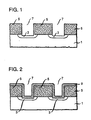
- FIG. 1 shows substrate 1, contact regions 3, and dielectric layer 5, with openings 7 exposing portions of regions 3; such openings typically are made by photolithographic processing involving etching in the presence of a patterned mask layer.
- Contact openings may be, e.g., to source or drain regions of field-effect transistors, or to contact regions intended for device interconnection. Typically, in the latter case, contact is made to silicon in polycrystalline form. Contact regions typically comprise heavily doped silicon, and they may further comprise a surface region of a silicide such as, e.g., titanium silicide which was formed prior to deposition of dielectric layer 5.
- the dielectric may consist essentially of an oxide.
- FIG. 2 shows the device of FIG. 1 after further processing involving the deposition of silicide-forming layer 9, exemplary device features 1, 3, 5, and 7 here and throughout being the same as in FIG. 1.
- Layer 9 may consist essentially of titanium, and deposition may be sputtering; the choice of material and of the deposition method is influenced by considerations of adhesion and step coverage. In the case of titanium, preferred thickness of layer 9 is in a range from 10 to 100 nanometers, 60 nanometers being typical.
- preferred processing calls for (rapid) thermal annealing in a non-oxidizing atmosphere such as, e.g., a nitrogen atmosphere; such annealing involves (short-term) heating at an elevated temperature, e.g., by exposure to infrared radiation.
- a non-oxidizing atmosphere such as, e.g., a nitrogen atmosphere
- preferred annealing is at a temperature in the range from 750 to 950 degrees C for a duration in the range from 10 seconds to 1 minute, lower temperatures corresponding to longer times and conversely.
- An exemplary temperature is approximately 800 degrees C, with a corresponding time of approximately 20 seconds.
- time and temperature may be chosen to effect substantial conversion of the material of layer 9 into (i) silicide adjacent to the substrate, and (ii) a conductive surface compound with an atmospheric constituent such as, e.g., nitrogen.
- a conductive surface compound with an atmospheric constituent such as, e.g., nitrogen.
- annealing fosters replenishment of silicide lost in the course of window etching.
- annealing may result in the removal of surface oxides and contaminants.
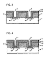
- FIG. 3 shows the device of FIG. 2 after annealing, layer 9 now comprising sublayers 91, 92, and 93.
- Layer 91 consists essentially of silicide as formed due to reaction of deposited silicide-forming material with silicon
- layer 92 consists essentially of unreacted silicide-forming material
- layer 93 consists essentially of a nitride of the silicide-forming material, as illustrative of the case in which the annealing atmosphere comprises nitrogen.
- FIG. 4 shows the device of FIG. 3 after further deposition of a metallization layer 11, typically consisting essentially of aluminum comprising a small amount of silicon or copper, and having a thickness which is in a typical range from 400 nanometers to 1.2 micrometers. At this point, the device is ready for further processing as is well-understood in the art.
- a metallization layer 11 typically consisting essentially of aluminum comprising a small amount of silicon or copper, and having a thickness which is in a typical range from 400 nanometers to 1.2 micrometers.
- CMOS complementary metal-oxide semiconductor
- CMOS complementary metal-oxide semiconductor
- a conductive compound can further serve as a built-in safeguard and electrical path in case of interruption of the metallization due to electromigration.
- Processing of the invention may also involve metallization metals other than aluminum, tungsten being considered a particularly suitable alternative.
- a deposited silicide-forming material may be alloyed not only with the underlying silicon, but also with the metallization, and this will apply especially in the case of a tungsten metallization.
- materials other than titanium suitable as a silicide-forming material, are cobalt, platinum, and alloys of titanium, cobalt, and platinum.
- nitrogen suitable as an inert atmospheric constituent during annealing, argon or helium may be used, as well as mixtures of such gases.
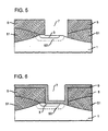
- FIG. 5-8 show field oxide 51 and doped region 52.
- substrate 1 is p-doped
- region 52 is doped n+, e.g., with arsenic and/or phosphorus.
- the substrate is n-doped
- region 52 is doped p+, e.g., with boron.
- window 7 is shown etched such that not only a portion of silicide region 3 is uncovered but, due to (unintended) misalignment, also a portion of substrate 1.
- window 7 is shown etched such that not only a portion of silicide region 3 is uncovered but, due to (unintended) misalignment, also a portion of substrate 1.
- such latter portion would be ineffective as part of the intended contact, and its presence would lead to shorting between a doped tub in the substrate and a source or drain contact.
- Such inefficacy and shorting are prevented by preferred processing in accordance with the invention in that the junction is extended essentially coextensive with the window as etched.
- silicide-forming layer 9 (FIG. 6), and as a result of annealing (FIG. 7), impurities have diffused laterally, resulting in extension of doped region 52.
- arsenic is preferred as n-type dopant on account of its high diffusivity in silicide.
- silicide 91 extends over the newly doped region, thereby resulting in the formation of an efficacious contact in spite of misalignment of the window.
- the final structure including metallization layer 11 is shown in FIG. 8.
- CMOS complementary metal-oxide semiconductor
- NMOS-dominated devices such as, e.g., dynamic random-access memory (DRAM) arrays.
- DRAM dynamic random-access memory
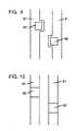
- preferred processing may permit the use of so-called headless contacts to active areas whose width is the same as the window width -- thus permitting the use of more narrow active areas, and closer spacing of active areas on a chip. This is illustrated by FIG. 9 and 10 which show two adjacent active areas 81, and windows 82.
- windows 82 are etched at widened portions of the active area 81 as is typical in prior-art practice. Widened areas are included to provide a margin of window misalignment relative to the active area, as well as a margin of window oversize as may occur during window patterning.
- FIG. 10 illustrates the use of an active area 81 which nominally has the same width as windows 82, as made practicable due to processing in accordance with the invention, potential window misalignment or oversize being compensated for by extension of the junction as described above. It is readily apparent upon inspection of FIG. 9 and 10 that, given a specified window size and a specified minimum distance between adjacent active areas, less space is occupied by the active areas in FIG. 10 as compared with FIG. 9.
Landscapes
- Electrodes Of Semiconductors (AREA)
- Internal Circuitry In Semiconductor Integrated Circuit Devices (AREA)
- Insulated Gate Type Field-Effect Transistor (AREA)
Applications Claiming Priority (2)
| Application Number | Priority Date | Filing Date | Title |
|---|---|---|---|
| US35945089A | 1989-05-31 | 1989-05-31 | |
| US359450 | 2003-02-06 |
Publications (2)
| Publication Number | Publication Date |
|---|---|
| EP0400877A2 true EP0400877A2 (fr) | 1990-12-05 |
| EP0400877A3 EP0400877A3 (fr) | 1991-10-23 |
Family
ID=23413839
Family Applications (1)
| Application Number | Title | Priority Date | Filing Date |
|---|---|---|---|
| EP19900305583 Ceased EP0400877A3 (fr) | 1989-05-31 | 1990-05-23 | Métallisation de contact de dipositifs de semi-conducteur de circuit intégré |
Country Status (2)
| Country | Link |
|---|---|
| EP (1) | EP0400877A3 (fr) |
| JP (1) | JPH0329321A (fr) |
Cited By (3)
| Publication number | Priority date | Publication date | Assignee | Title |
|---|---|---|---|---|
| EP0607820A3 (fr) * | 1993-01-08 | 1994-12-28 | Nippon Electric Co | Procédé de fabrication d'un dispositif semi-conducteur comportant une couche de siliciure métallique sur une région diffusée. |
| EP0851493A1 (fr) * | 1996-12-27 | 1998-07-01 | STMicroelectronics S.r.l. | Structure de contact pour dispositifs semi-conducteurs électroniques EPROM ou flash EPROM et méthode de fabrication |
| WO2001004947A1 (fr) * | 1999-07-12 | 2001-01-18 | Advanced Micro Devices, Inc. | Rattrapage de la perte de materiau dans une couche de siliciure metallique au niveau des contacts de dispositifs a circuits imprimes |
Families Citing this family (3)
| Publication number | Priority date | Publication date | Assignee | Title |
|---|---|---|---|---|
| KR940006689B1 (ko) * | 1991-10-21 | 1994-07-25 | 삼성전자 주식회사 | 반도체장치의 접촉창 형성방법 |
| JPH0837164A (ja) * | 1994-07-21 | 1996-02-06 | Nec Corp | 半導体装置の製造方法 |
| KR100357186B1 (ko) * | 2000-11-02 | 2002-10-19 | 주식회사 하이닉스반도체 | 반도체 소자의 콘택 형성방법 |
Family Cites Families (1)
| Publication number | Priority date | Publication date | Assignee | Title |
|---|---|---|---|---|
| JPS61206243A (ja) * | 1985-03-08 | 1986-09-12 | Mitsubishi Electric Corp | 高融点金属電極・配線膜を用いた半導体装置 |
-
1990
- 1990-05-23 EP EP19900305583 patent/EP0400877A3/fr not_active Ceased
- 1990-05-30 JP JP2138657A patent/JPH0329321A/ja active Pending
Cited By (5)
| Publication number | Priority date | Publication date | Assignee | Title |
|---|---|---|---|---|
| EP0607820A3 (fr) * | 1993-01-08 | 1994-12-28 | Nippon Electric Co | Procédé de fabrication d'un dispositif semi-conducteur comportant une couche de siliciure métallique sur une région diffusée. |
| EP0851493A1 (fr) * | 1996-12-27 | 1998-07-01 | STMicroelectronics S.r.l. | Structure de contact pour dispositifs semi-conducteurs électroniques EPROM ou flash EPROM et méthode de fabrication |
| US6124169A (en) * | 1996-12-27 | 2000-09-26 | Stmicroelectronics, S.R.L. | Contact structure and associated process for production of semiconductor electronic devices and in particular nonvolatile EPROM and flash EPROM memories |
| WO2001004947A1 (fr) * | 1999-07-12 | 2001-01-18 | Advanced Micro Devices, Inc. | Rattrapage de la perte de materiau dans une couche de siliciure metallique au niveau des contacts de dispositifs a circuits imprimes |
| US6271122B1 (en) | 1999-07-12 | 2001-08-07 | Advanced Micro Devices, Inc. | Method of compensating for material loss in a metal silicone layer in contacts of integrated circuit devices |
Also Published As
| Publication number | Publication date |
|---|---|
| JPH0329321A (ja) | 1991-02-07 |
| EP0400877A3 (fr) | 1991-10-23 |
Similar Documents
| Publication | Publication Date | Title |
|---|---|---|
| US5102827A (en) | Contact metallization of semiconductor integrated-circuit devices | |
| US4333099A (en) | Use of silicide to bridge unwanted polycrystalline silicon P-N junction | |
| US4648175A (en) | Use of selectively deposited tungsten for contact formation and shunting metallization | |
| US3906540A (en) | Metal-silicide Schottky diode employing an aluminum connector | |
| CA1207469A (fr) | Methode de fabrication de transistors mos | |
| JP2569327B2 (ja) | シリコンベースの半導体装置のためのコンタクト構造 | |
| JP3066041B2 (ja) | 高い抵抗性の無定形シリコン抵抗器を含む集積回路を形成する方法 | |
| US5340751A (en) | Method of manufacturing a BiMOS device | |
| US5457062A (en) | Method for forming gigaohm load for BiCMOS process | |
| JPS61501358A (ja) | 中間金属シリサイド層を有する改良型集積回路構造およびその製作方法 | |
| JP3626773B2 (ja) | 半導体デバイスの導電層、mosfet及びそれらの製造方法 | |
| US5091322A (en) | Semiconductor device and method of manufacturing the same | |
| US4729969A (en) | Method for forming silicide electrode in semiconductor device | |
| US6495460B1 (en) | Dual layer silicide formation using a titanium barrier to reduce surface roughness at silicide/junction interface | |
| JPS592186B2 (ja) | 相補型mos装置 | |
| JPH0837164A (ja) | 半導体装置の製造方法 | |
| EP0400877A2 (fr) | Métallisation de contact de dipositifs de semi-conducteur de circuit intégré | |
| JP3093620B2 (ja) | 半導体装置の製造方法 | |
| US4476157A (en) | Method for manufacturing schottky barrier diode | |
| US5521416A (en) | Semiconductor device having gate electrode and impurity diffusion layer different in conductivity type and method of manufacturing the same | |
| KR100289372B1 (ko) | 폴리사이드 형성방법 | |
| KR0151038B1 (ko) | 반도체장치의 폴리사이드 콘택 및 그 형성방법 | |
| JP3253438B2 (ja) | 半導体装置 | |
| US20020068444A1 (en) | Dual layer silicide formation using an aluminum barrier to reduce surface roughness at silicide/junction interface | |
| JP3292154B2 (ja) | 半導体装置の製造方法 |
Legal Events
| Date | Code | Title | Description |
|---|---|---|---|
| PUAI | Public reference made under article 153(3) epc to a published international application that has entered the european phase |
Free format text: ORIGINAL CODE: 0009012 |
|
| AK | Designated contracting states |
Kind code of ref document: A2 Designated state(s): DE ES FR GB IT NL |
|
| PUAL | Search report despatched |
Free format text: ORIGINAL CODE: 0009013 |
|
| AK | Designated contracting states |
Kind code of ref document: A3 Designated state(s): DE ES FR GB IT NL |
|
| 17P | Request for examination filed |
Effective date: 19920415 |
|
| RAP3 | Party data changed (applicant data changed or rights of an application transferred) |
Owner name: AT&T CORP. |
|
| 17Q | First examination report despatched |
Effective date: 19940614 |
|
| STAA | Information on the status of an ep patent application or granted ep patent |
Free format text: STATUS: THE APPLICATION HAS BEEN REFUSED |
|
| 18R | Application refused |
Effective date: 19950403 |