EP0400982A2 - Diode éléctroluminescente et méthode de fabrication - Google Patents
Diode éléctroluminescente et méthode de fabrication Download PDFInfo
- Publication number
- EP0400982A2 EP0400982A2 EP90305865A EP90305865A EP0400982A2 EP 0400982 A2 EP0400982 A2 EP 0400982A2 EP 90305865 A EP90305865 A EP 90305865A EP 90305865 A EP90305865 A EP 90305865A EP 0400982 A2 EP0400982 A2 EP 0400982A2
- Authority
- EP
- European Patent Office
- Prior art keywords
- light
- epitaxial layers
- thickness
- layer
- emitting diode
- Prior art date
- Legal status (The legal status is an assumption and is not a legal conclusion. Google has not performed a legal analysis and makes no representation as to the accuracy of the status listed.)
- Ceased
Links
Images

Classifications
-
- H—ELECTRICITY
- H10—SEMICONDUCTOR DEVICES; ELECTRIC SOLID-STATE DEVICES NOT OTHERWISE PROVIDED FOR
- H10H—INORGANIC LIGHT-EMITTING SEMICONDUCTOR DEVICES HAVING POTENTIAL BARRIERS
- H10H20/00—Individual inorganic light-emitting semiconductor devices having potential barriers, e.g. light-emitting diodes [LED]
- H10H20/80—Constructional details
- H10H20/81—Bodies
- H10H20/822—Materials of the light-emitting regions
- H10H20/824—Materials of the light-emitting regions comprising only Group III-V materials, e.g. GaP
-
- H—ELECTRICITY
- H10—SEMICONDUCTOR DEVICES; ELECTRIC SOLID-STATE DEVICES NOT OTHERWISE PROVIDED FOR
- H10H—INORGANIC LIGHT-EMITTING SEMICONDUCTOR DEVICES HAVING POTENTIAL BARRIERS
- H10H20/00—Individual inorganic light-emitting semiconductor devices having potential barriers, e.g. light-emitting diodes [LED]
- H10H20/01—Manufacture or treatment
- H10H20/011—Manufacture or treatment of bodies, e.g. forming semiconductor layers
- H10H20/013—Manufacture or treatment of bodies, e.g. forming semiconductor layers having light-emitting regions comprising only Group III-V materials
-
- Y—GENERAL TAGGING OF NEW TECHNOLOGICAL DEVELOPMENTS; GENERAL TAGGING OF CROSS-SECTIONAL TECHNOLOGIES SPANNING OVER SEVERAL SECTIONS OF THE IPC; TECHNICAL SUBJECTS COVERED BY FORMER USPC CROSS-REFERENCE ART COLLECTIONS [XRACs] AND DIGESTS
- Y10—TECHNICAL SUBJECTS COVERED BY FORMER USPC
- Y10S—TECHNICAL SUBJECTS COVERED BY FORMER USPC CROSS-REFERENCE ART COLLECTIONS [XRACs] AND DIGESTS
- Y10S148/00—Metal treatment
- Y10S148/095—Laser devices
Definitions
- the present invention relates to a light-emitting diode constituted by a compound semiconductor single crystal GaAs 1-x P x (0 ⁇ x ⁇ 1) and to a process for preparing a starting wafer for the light-emitting diode.
- a compound semiconductor structure having a p-n junction formed therein emits light when forward biased. This characteristic is used for preparation of light-emitting diodes from compound semiconductors.
- Such a technology is disclosed, for instance, in Japanese Patent Examined Publication No. 60-57214.
- the constant composition epitaxial layer stated above includes a light-emitting nitrogen-doped layer which further contains p-type layer diffused, for instance, with Zn.
- the present invention was made according to this novel discovery.
- a light-emitting diode having alloyed compound semiconductor epitaxial layers constituted by GaAs 1-x P x (0 ⁇ x ⁇ 1) on a compound semiconductor single-crystal substrate and having a light emitting layer provided with a p-n junction formed in a surface layer region of said epitaxial layers has said epitaxial layers being set at 20 to 40 ⁇ m in total thickness.
- the total thickness of the epitaxial layers stated above is determined to be 20 ⁇ m to 40 ⁇ m. This reduces the amount of optical absorption within the bulk of the epitaxial layers compared to conventional epitaxial layer thicknesses of about 50 to 100 ⁇ m and at the same time reduces the time and costs for preparing an epitaxial wafer.
- the light-emitting diode of the preferred embodiments has a GaP layer (buffer layer) 2 which is an epitaxial layer formed directly on a GaP substrate 1.
- the Gap layer (buffer layer) 2 is grown epitaxially directly on the GaP substrate 1, because a graded alloy composition layer 3 (described later) deposited directly on the GaP substrate 1 will often cause the crystallinity in the graded alloy composition layer 3 to be in disorder due to the lattice mismatch between the substrate 1 and the layer 3. Consequently, a graded alloy composition layer 3 constituted by an epitaxial layer is formed on GaP layer 2.
- This graded alloy composition epitaxial layer 3 is represented by a general expression, GaAs 1-x P x .
- the value x in this expression depends upon the emission light wavelengths of the light-emitting diode. For yellow emission, for instance, the value x is controlled to vary gradually form 1 to 0.85.
- the second same constant composition GaAs 1-x P x (x constant) epitaxial layer 5.
- This layer 5 is grown by gradually increasing the amount of NH3 in the reactant gas stream so that the doped amount of N can be gradually increased in the crystal layer 5.
- the third same constant composition GaAs 1-x P x (x constant) epitaxial layer 6, which is doped with a constant ratio of nitrogen. It is to be noted that the constant composition epitaxial layers 4, 5, 6 have a value x, for instance, of 0.85 for yellow emission.
- the third constant composition epitaxial layer 6 of n-type is diffused with Zn from the surface thereof to form a p-type impurity diffused layer within the surface region of the layer 6, thereby the third constant composition epitaxial layer 6 can be constituted to perform a function as a light-emitting layer with the p-n junction in it.
- the constant composition epitaxial layer 6 is constituted to have a thickness 10 ⁇ m and more so that the function of the layer 6 as a light-emitting layer is not impaired.
- the total thickness x0 of the epitaxial layers 2, 3, 4, 5, 6 is adjusted to be 40 ⁇ m or less. This total thickness x0 of the epitaxial layers should preferably be minimal so that the thickness is as large as does not deteriorate the light-emitting power of a light-emitting diode.
- the reason the thickness of the constant composition epitaxial layer 6 is set at 10 ⁇ m and more is that the thicknesses less than 10 ⁇ m prevent the good p-n junction from being formed within the layer 6, with an adverse possi bility that the function of light emission which the layer 6 has may be impaired.
- the reason the total thickness x0 of the epitaxial layers is set at 40 ⁇ m and less is that such a thickness allows the amount of optical absorption within the epitaxial layers to be made small, with the result that a sufficient light output power can be obtained.
- a GaP layer (buffer layer) 2 is formed on a GaP substrate 1 by means of an epitaxial growth process.
- a graded alloy composition GaAs 1-x P x epitaxial layer 3 is formed by the epitaxial growth process.
- a constant composition epitaxial layer 4 is formed by the epitaxial growth process.
- a constant composition GaAs 1-x P x epitaxial layer 5 is grown on the layer 4 by the epitaxial growth method with the amount of nitrogen added being increased gradiently.
- a constant composition GaAs 1-x P x epitaxial layer 6 is for:ned on the layer 5 by the epitaxial growth method with the amount of nitrogen added being kept constant.
- the constant composition epitaxial layer 6 of n-type is diffused with Zn, a p-type impurity, from the surface thereof to form a p-type layer within the layer 6. Further, electrodes are formed.
- the total thickness of the epitaxial layers is set at 40 ⁇ m or less; the thickness of the constant composition epitaxial layer 6 is set at 15 ⁇ m.
- the epitaxial layers which have been grown thick enough can be controlled in thickness by means of chemical etching the layer 6 so that the thickness of the epitaxial layers and the constant composition layer 6 can be adjusted.
- Light-emitting diodes thus obtained permit the optical absorption within the epitaxial layers to be reduced, with the consequence that diodes with high light output power can be produced.
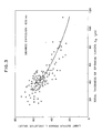
- Fig. 3 sets of the data from the experiments mentioned above are shown in X-Y coordinates with respect to the total thickness of the epitaxial layers x0 and light output power L and further, the equation of approximation obtained above is drawn in a solid line among the plotting of the data for comparison.
- the light-emitting diode used for the same experiments are of orange emission, and therefore the constant composition epitaxial layer 6 is composed of a mixed crystal GaAs 0.35 P 0.65 .
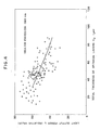
- Fig. 4 shows another set of the data from the same experiments as those for Fig. 3. And in the figure, another equation of approximation is shown with the data above plotted.
- the light-emitting diode used in the case of Fig. 4, that is, the constant epitaxial layer 6 is composed of GaAs 0.15 P 0.85 and the same diode emits yellow light.
- Figs. 3 and 4 show that the less the total thickness of the epitaxial layers, the higher the light output power L (relative values) becomes.
- the light output power L (relative values) obtained from the approximation is practically consistent with the experimental results as shown in Figs. 3 and 4. This also confirms that the above approximate equations hold.
- the total thickness of 40 ⁇ m of the epitaxial layers allows the light output power to be maximum. If the total epitaxial layer thickness is decreased toward less than 40 ⁇ m, the light output power becomes lower than the light output power presumed from the approximate equations stated above. Instead, the light output power shows a downward trend for the thickness less than 40 ⁇ m. But at as lower as 20 ⁇ m, the light output still observed is roughly the same level as that at around 40 ⁇ m. Consequently, Figs. 3 and 4 show that the thickness of the epitaxial layers is preferably chosen to be 20 to 40 ⁇ m.
- the total thickness of the epitaxial layers should be set at 20 to 40 ⁇ m with tho thickness of the constant composition layers ranging form 10 to 20 ⁇ m.
- a 20 ⁇ m thickness of the constant composition layers corresponds to a 40 ⁇ m thickness of the total epitaxial layers.
- the application of the above mentioned equations of approximation enables the thickness of the other epitaxial layers to be estimated through some experiments carried out in consideration of the established relationship between the thickness of epitaxial layers and the light output power at the time of the preparation of compound semiconductor wafers for light-emitting diodes.
- a maximum allowable value of a particular or whole epitaxial layer thickness can be obtained relative to a determined light output power. It is possible that the allowable value of thicknass thus obtained is utilized as an effective guide for light-emitting diode manufacture, within which a graded composition epitaxial layer shall be successfully prepared to improve the crystallinity of the constant epitaxial layers to the utmost extent.
- the less total thickness of the epitaxial layers x0 enables the throughput in the production line to be improved in accordance with the extent of tha curtailed thickness.
- the relationship between the total epitaxial layer thicknass x0, the period of time required for the formation of epitaxial layers, and the light output power L is shown in Table 2, In the table, letter n denotes the number of wafers and letter ⁇ denotes the variations in the thickness and the light output power.
- GaP is used for a substrate according to the preferred embodiments of the present invention.
- This technique according to the preferred embodiments can also be applied to a GaAs substrate.
- the application of the preferred embodiments according to the present invention is not restricted to light-emitting diodes prepared by vapor phase growth to be employed mainly for compound semiconductor epitaxial growth, but also extended to liquid phase growth.
Landscapes
- Led Devices (AREA)
Applications Claiming Priority (2)
| Application Number | Priority Date | Filing Date | Title |
|---|---|---|---|
| JP138355/89 | 1989-05-30 | ||
| JP1138355A JPH06105796B2 (ja) | 1989-05-30 | 1989-05-30 | 発光ダイオードおよびその製造方法 |
Publications (2)
| Publication Number | Publication Date |
|---|---|
| EP0400982A2 true EP0400982A2 (fr) | 1990-12-05 |
| EP0400982A3 EP0400982A3 (fr) | 1991-01-23 |
Family
ID=15219998
Family Applications (1)
| Application Number | Title | Priority Date | Filing Date |
|---|---|---|---|
| EP19900305865 Ceased EP0400982A3 (fr) | 1989-05-30 | 1990-05-30 | Diode éléctroluminescente et méthode de fabrication |
Country Status (3)
| Country | Link |
|---|---|
| US (1) | US5057442A (fr) |
| EP (1) | EP0400982A3 (fr) |
| JP (1) | JPH06105796B2 (fr) |
Families Citing this family (4)
| Publication number | Priority date | Publication date | Assignee | Title |
|---|---|---|---|---|
| US5445897A (en) * | 1989-11-22 | 1995-08-29 | Mitsubishi Kasei Polytec Company | Epitaxial wafer and process for producing the same |
| JP3111644B2 (ja) * | 1992-06-09 | 2000-11-27 | 三菱化学株式会社 | りん化ひ化ガリウムエピタキシャルウエハ |
| JP3143040B2 (ja) * | 1995-06-06 | 2001-03-07 | 三菱化学株式会社 | エピタキシャルウエハおよびその製造方法 |
| JP3854693B2 (ja) * | 1996-09-30 | 2006-12-06 | キヤノン株式会社 | 半導体レーザの製造方法 |
Family Cites Families (11)
| Publication number | Priority date | Publication date | Assignee | Title |
|---|---|---|---|---|
| JPS5539913B2 (fr) * | 1972-11-06 | 1980-10-14 | ||
| JPS589362B2 (ja) * | 1978-03-10 | 1983-02-21 | 旭化成株式会社 | 赤外線多層フイルム膜厚測定方法及びその測定装置 |
| JPS6057214A (ja) * | 1983-09-09 | 1985-04-03 | Hitachi Ltd | 電磁流量計励磁回路 |
| US4695162A (en) * | 1984-05-24 | 1987-09-22 | Victor Company Of Japan, Ltd. | Film thickness measuring apparatus |
| JPS6129562A (ja) * | 1984-07-20 | 1986-02-10 | Sanyo Electric Co Ltd | 印字用発光ダイオ−ド |
| JPS61291491A (ja) * | 1985-06-19 | 1986-12-22 | Mitsubishi Monsanto Chem Co | りん化ひ化ガリウム混晶エピタキシヤルウエハ |
| JPS6273687A (ja) * | 1985-09-26 | 1987-04-04 | Mitsubishi Electric Corp | 半導体レ−ザ装置 |
| US4787749A (en) * | 1985-11-28 | 1988-11-29 | Canon Kabushiki Kaisha | Method and apparatus for measuring the thickness of a thin film using the spectral reflection factor of the film |
| JPS6458457A (en) * | 1987-08-31 | 1989-03-06 | Okuma Machinery Works Ltd | Nc machine tool equipped with high speed response type fine positioning device |
| US4893313A (en) * | 1988-03-14 | 1990-01-09 | Kabushiki Kaisha Toshiba | Semiconductor laser device which has a double-hetero structure having an optimal layer thickness |
| JPH0252205A (ja) * | 1988-08-17 | 1990-02-21 | Dainippon Screen Mfg Co Ltd | 膜厚測定方法 |
-
1989
- 1989-05-30 JP JP1138355A patent/JPH06105796B2/ja not_active Expired - Lifetime
-
1990
- 1990-05-30 US US07/530,876 patent/US5057442A/en not_active Expired - Fee Related
- 1990-05-30 EP EP19900305865 patent/EP0400982A3/fr not_active Ceased
Also Published As
| Publication number | Publication date |
|---|---|
| JPH06105796B2 (ja) | 1994-12-21 |
| JPH033275A (ja) | 1991-01-09 |
| US5057442A (en) | 1991-10-15 |
| EP0400982A3 (fr) | 1991-01-23 |
Similar Documents
| Publication | Publication Date | Title |
|---|---|---|
| EP0599224B2 (fr) | Dispositif émetteur de lumière comprenant des composés à base de nitrure de gallium | |
| US7071015B2 (en) | Semiconductor light emitting device and method for producing the same | |
| US5932896A (en) | Nitride system semiconductor device with oxygen | |
| US7899101B2 (en) | Semiconductor light emitting device and manufacturing method therefor | |
| US6495894B2 (en) | Photonic device, a substrate for fabricating a photonic device, a method for fabricating the photonic device and a method for manufacturing the photonic device-fabricating substrate | |
| EP0214610A2 (fr) | Galette semi-conductrice en arséniure de gallium épitaxial et méthode pour la produire | |
| EP0378919A2 (fr) | Dispositif opto-électronique à large bande interdite et méthode de fabrication | |
| US20040021142A1 (en) | Light emitting diode device | |
| US5103270A (en) | Double hetero type epitaxial wafer with refractive indices | |
| US5057442A (en) | Process for preparing light-emitting diodes using a maximum layer thickness equation | |
| EP0293000B1 (fr) | Dispositif émetteur de lumière | |
| US5912476A (en) | Compound semiconductor epitaxial wafer | |
| EP0544357B1 (fr) | Diode semiconductrice émettrice de rayonnement | |
| US5534717A (en) | Epitaxial wafer for light-emitting diode | |
| JPH09199757A (ja) | 化合物半導体エピタキシャルウエーハ | |
| Holonyak Jr et al. | III-V Semiconductor Quantum Well Lasers and Related Optoelectronic Devices on Silicon (Abstracts) | |
| JPH11330544A (ja) | Iii族窒化物半導体発光素子 | |
| JPH06252439A (ja) | 面発光型発光ダイオードおよびその製造方法 |
Legal Events
| Date | Code | Title | Description |
|---|---|---|---|
| PUAI | Public reference made under article 153(3) epc to a published international application that has entered the european phase |
Free format text: ORIGINAL CODE: 0009012 |
|
| AK | Designated contracting states |
Kind code of ref document: A2 Designated state(s): DE FR GB |
|
| PUAL | Search report despatched |
Free format text: ORIGINAL CODE: 0009013 |
|
| AK | Designated contracting states |
Kind code of ref document: A3 Designated state(s): DE FR GB |
|
| 17P | Request for examination filed |
Effective date: 19910228 |
|
| 17Q | First examination report despatched |
Effective date: 19921028 |
|
| STAA | Information on the status of an ep patent application or granted ep patent |
Free format text: STATUS: THE APPLICATION HAS BEEN REFUSED |
|
| 18R | Application refused |
Effective date: 19940418 |