EP0401113B1 - Dispositif semi-conducteur et son procédé de fabrication - Google Patents
Dispositif semi-conducteur et son procédé de fabrication Download PDFInfo
- Publication number
- EP0401113B1 EP0401113B1 EP90401446A EP90401446A EP0401113B1 EP 0401113 B1 EP0401113 B1 EP 0401113B1 EP 90401446 A EP90401446 A EP 90401446A EP 90401446 A EP90401446 A EP 90401446A EP 0401113 B1 EP0401113 B1 EP 0401113B1
- Authority
- EP
- European Patent Office
- Prior art keywords
- transistor
- semiconductor
- layer
- type
- side wall
- Prior art date
- Legal status (The legal status is an assumption and is not a legal conclusion. Google has not performed a legal analysis and makes no representation as to the accuracy of the status listed.)
- Expired - Lifetime
Links
Images




Classifications
-
- H—ELECTRICITY
- H10—SEMICONDUCTOR DEVICES; ELECTRIC SOLID-STATE DEVICES NOT OTHERWISE PROVIDED FOR
- H10B—ELECTRONIC MEMORY DEVICES
- H10B12/00—Dynamic random access memory [DRAM] devices
- H10B12/30—DRAM devices comprising one-transistor - one-capacitor [1T-1C] memory cells
- H10B12/31—DRAM devices comprising one-transistor - one-capacitor [1T-1C] memory cells having a storage electrode stacked over the transistor
-
- H—ELECTRICITY
- H10—SEMICONDUCTOR DEVICES; ELECTRIC SOLID-STATE DEVICES NOT OTHERWISE PROVIDED FOR
- H10D—INORGANIC ELECTRIC SEMICONDUCTOR DEVICES
- H10D1/00—Resistors, capacitors or inductors
- H10D1/60—Capacitors
- H10D1/68—Capacitors having no potential barriers
-
- H—ELECTRICITY
- H10—SEMICONDUCTOR DEVICES; ELECTRIC SOLID-STATE DEVICES NOT OTHERWISE PROVIDED FOR
- H10B—ELECTRONIC MEMORY DEVICES
- H10B12/00—Dynamic random access memory [DRAM] devices
- H10B12/01—Manufacture or treatment
- H10B12/02—Manufacture or treatment for one transistor one-capacitor [1T-1C] memory cells
- H10B12/03—Making the capacitor or connections thereto
- H10B12/033—Making the capacitor or connections thereto the capacitor extending over the transistor
-
- H—ELECTRICITY
- H10—SEMICONDUCTOR DEVICES; ELECTRIC SOLID-STATE DEVICES NOT OTHERWISE PROVIDED FOR
- H10B—ELECTRONIC MEMORY DEVICES
- H10B12/00—Dynamic random access memory [DRAM] devices
- H10B12/01—Manufacture or treatment
- H10B12/02—Manufacture or treatment for one transistor one-capacitor [1T-1C] memory cells
- H10B12/03—Making the capacitor or connections thereto
- H10B12/033—Making the capacitor or connections thereto the capacitor extending over the transistor
- H10B12/0335—Making a connection between the transistor and the capacitor, e.g. plug
Definitions
- the present invention generally relates to semiconductor devices and production methods thereof, and more particularly to a semiconductor device having first and second transistors and a production method thereof, where there are three demands on the first and second transistors.
- First there is a demand to suppress generation of crystal defect in the first transistor by not subjecting an impurity diffusion layer of the first transistor to an etching.
- Second there is a demand to form a conductor layer on the first transistor via an insulator layer.
- DRAM dynamic random access memory
- a first condition is not to subject an impurity diffusion layer of a transistor which makes up the memory cell so as to suppress the generation of crystal defect.
- a second condition is to facilitate the formation of a storage electrode by flattening a layer below the storage electrode.
- a third condition is to ensure a satisfactory current driving capability of the transistor of a peripheral circuit.
- EP-A-0 191 612 disclosing a DRAM device.
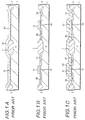
- FIG.1K shows a cross section of an essential part of this conventional DRAM.
- the DRAM includes a p-type silicon (Si) substrate 1, a field oxide layer 2 which forms a device isolation region, a memory cell 3, and a peripheral circuit 4.
- the memory cell 3 is made up of an n-channel insulated-gate type field effect transistor (hereinafter simply referred to as an nMOS FET) 5 which forms a transistor for controlling input/output of charge, and a stacked capacitor 6.
- the nMOS FET 5 has a lightly doped drain (LDD) structure.
- a source diffusion layer 7 of the nMOS FET 5 is made up of an n - -type source diffusion layer 8 and an n + -type source diffusion layer 9.
- a drain diffusion layer 10 of the nMOS FET 5 is made up of an n - -type drain diffusion layer 11 and an n + -type drain diffusion layer 12.
- a gate insulator layer 13 is made of silicon dioxide (SiO 2 ), a gate electrode (word line) 14 is made of polysilicon, an interlayer insulator 15 is made of SiO 2 , an interlayer insulator 16 is made of phospho-silicate glass (PSG), and a bit line 17 is made of aluminum (Al).
- the bit line 17 makes an ohmic contact with the n + -type source diffusion layer 9 via a contact hole 18.
- the stacked capacitor 6 is made up of a stacked structure including a polysilicon storage electrode 19, a SiO 2 capacitor insulator layer 20 and a polysilicon confronting electrode 21.
- the storage electrode 19 makes an ohmic contact with the n + -type drain diffusion layer 12 via a contact hole 22.
- the peripheral circuit 4 is made up of an nMOS FET 23 which also has the LDD structure.
- a source diffusion layer 24 of the nMOS FET 23 is made up of an n - -type source diffusion layer 25 and an n + -type source diffusion layer 26.
- a drain diffusion layer 27 of the nMOS FET 23 is made up of an n - -type drain diffusion layer 28 and an n + -type drain diffusion layer 29.
- a gate insulator layer 30 is made of SiO 2
- a gate electrode 31 is made of polysilicon
- an interconnection 32 is made of Al. The interconnection 32 makes an ohmic contact with the n + -type drain diffusion layer 29 via a contact hole 33.
- bit line 17 makes an ohmic contact with the n + -type source diffusion layer 26 via a contact hole 34.
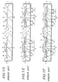
- This conventional DRAM is produced in a sequence shown in FIGS.1A through 1K.
- the p-type Si substrate 1 is prepared as shown in FIG.1A.
- the SiO 2 layers 13 and 30 are formed in a device region by a thermal oxidation to a thickness of 150 ⁇ , for example.
- CVD chemical vapor deposition
- the polysilicon layer 35 is patterned, and as shown in FIG.1B, the gate electrodes 14 and 31 are formed. Then, the gate electrodes 14 and 31 and the field oxide layer 2 are used as a mask when implanting phosphorous (P) ions into the p-type Si substrate 1 with an energy of 50 keV and a dosage of 1 x 10 13 cm -2 , for example. As a result, n - -type diffusion layers 36-39 are formed.
- P phosphorous
- a reactive ion etching (RIE) is made with respect to the SiO 2 layer 40 and the SiO 2 layers 13 and 30 under the SiO 2 layer 40, so as to partially expose the n - -type diffusion layers 36, 37, 38 and 39 as shown in FIG.1D.
- RIE reactive ion etching
- a thermal oxidation is made to form a SiO 2 layer 45 which has a thickness of 150 ⁇ , for example, on the exposed surfaces of the p-type Si substrate 1 and the gate electrodes 14 and 31 as shown in FIG.1E.
- the gate electrodes 14 and 31, the side wall SiO 2 layers 41, 42, 43 and 44 and the field oxide layer 2 are used as a mask when implanting arsenic (As) ions into the p-type Si substrate 1 with an energy of of 50 keV and a dosage of 4 x 10 15 cm -2 , for example.
- As arsenic
- the nMOS FET 5 has the source diffusion layer 7 which is made up of the n - -type source diffusion layer 8 and the n + -type source diffusion layer 9, and the drain diffusion layer 10 which is made up of the n - -type drain diffusion layer 11 and the n + -type drain diffusion layer 12.
- the nMOS FET 23 has the source diffusion layer 24 which is made up of the n - -type source diffusion layer 25 and the n + -type source diffusion layer 26, and the drain diffusion layer 27 which is made up of the n - -type drain diffusion layer 28 and the n + -type drain diffusion layer 29.
- an oxide layer which is naturally formed on the exposed surface of the storage electrode 19 is removed by an etching using a hydrogen fluoride (HF) solution. Further, a thermal oxidation is carried out to form a SiO 2 capacitor insulator layer 20 which has a thickness of 100 ⁇ , for example, on the exposed surface of the storage electrode 19 as shown in FIG.1I.
- HF hydrogen fluoride
- the PSG layer 16 is formed on the entire surface of the stacked structure to a thickness of 5000 ⁇ , for example, as shown in FIG.1K.
- the contact holes 18, 33 and 34 are formed in the PSG layer 16, and the bit line 17 and the other interconnection 32 are formed. As a result, the conventional DRAM having the stacked capacitor 6 is obtained.
- the side wall SiO 2 layers 41 and 42 are formed on the side wall portions of the gate electrode 14 as shown in FIG.1D in order to realize the LDD structure of the nMOS FETs 5 and 23.
- the side wall SiO 2 layers 41 and 42 flatten the vertical stepped portions at the side wall portions of the gate electrode 14, and have a function of facilitating the formation of the storage electrode 19.
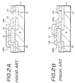
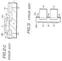
- FIGS.2A through 2C are cross sectional views and FIG.3 is a plan view for explaining the side wall SiO 2 layers 41 and 42.
- FIG.3 is a plan view for explaining the side wall SiO 2 layers 41 and 42.
- the storage electrode 19 is formed without forming the side wall SiO 2 layers 41 and 42 at the side wall portions of the gate electrode 14.
- a SiO 2 layer 48 which covers the gate electrode 14 and the n - -type diffusion layers 36 and 37 are first formed as shown in FIG.2A.
- the polysilicon layer 46 is formed on the entire surface of the stacked structure. Then, after the resistance of this polysilicon layer 46 is reduced by carrying out an ion implantation with respect to the polysilicon layer 46, an RIE is carried out and the polysilicon layer 46 is patterned to form the storage electrode 19 as shown in FIG.2B.
- side wall portions 48A and 48B of the SiO 2 layer 48 along the gate electrode 14 are formed vertically in accordance with the shape of the side wall portions of the gate electrode 14. For this reason, when the polysilicon layer 46 is etched by the RIE and the storage electrode 19 is formed as shown in FIG.2B, polysilicon (identified by reference numerals 50 and 51) remains at the side wall portions 48A and 48B of the SiO 2 layer 48 as shown in FIGS.2C and 3. For example, there is a problem in that the polysilicon 50 may extend across two mutually adjacent storage electrodes 19 and short-circuit these storage electrodes 19. On the other hand, there is a problem in that the polysilicon 51 may come off during a subsequent process and adhere across two mutually adjacent storage electrodes 19 and short-circuit these storage electrodes 19.
- the side wall portions of the gate electrode 14 may be formed as overhangs.
- the side wall portions 48A and 48B of the SiO 2 layer 48 are also formed as overhangs. For this reason, when the RIE is carried out with respect to the polysilicon layer 46 and the storage electrode 19 is formed, polysilicon inevitably remains at the side wall portions 48A and 48B.
- the side wall portions of the gate electrode 14 are formed as overhangs, the above described problems become particularly notable.
- the side wall SiO 2 layers 41 and 42 are formed at the side wall portions of the gate electrode 14 as shown in FIG.1D and the vertical stepped portions at the side wall portions of the gate electrode 14 are flattened so as to facilitate the formation of the storage electrode 19.
- the surface of the n - -type diffusion layer 37 is subjected to the plasma atmosphere.
- a crystal defect is generated at the surface of the n - -type diffusion layer 37 due to contamination of metals such as iron, copper and nickel which are included in the internal wall of a chamber containing the plasma or included in the plasma atmosphere caused by electrode erosion.
- the storage electrode 19 is connected to the surface of the n - -type diffusion layer 37, the charge storage characteristic (refresh characteristic) of the memory cell 3 is deteriorated by the crystal defect.
- the As ion implantation when forming the n + -type source diffusion layer 9, the n + -type drain diffusion layer 12, the n + -type source diffusion layer 26 and the n + -type drain diffusion layer 29 according to the conceivable method of FIG.4, it is necessary to accelerate the As ion implantation into the p-type Si substrate 1 such that the As ions penetrate the SiO 2 layer 52. But it is difficult to control the thickness of the SiO 2 layer 52 with a high accuracy according to the RIE, and the As ions must be implanted with an energy which takes into consideration the thickness distribution of the SiO 2 layer 52. Hence, when the As ion implantation is carried out under such consideration, the As ions penetrate the gate electrodes 14 and 31 and reach the channel region, thereby introducing undesirable effects on the characteristics of the nMOS FETs 5 and 23.
- the conventional DRAM shown in FIG.1K has the n + -type drain diffusion layer 12 provided in the nMOS FET 5, but the As ion implantation with respect to the p-type Si substrate 1 must be carried out with a high dosage in order to form this n + -type drain diffusion layer 12.
- the region which is subjected to the As ion implantation is transformed into an amorphous state, and it becomes necessary to thereafter carry out a thermal process to transform the region back into a crystal state.
- a dislocation loop is generated in the n + -type drain diffusion layer 12 and there is a problem in that the charge storage characteristic of the memory cell 3 is deteriorated thereby.
- the tip end of the side wall SiO 2 layer 42 makes direct contact with the p-type Si substrate 1 as shown in FIG.1D, and an angle the tip end of the side wall SiO 2 layer 42 makes with respect to the surface of the p-type Si substrate 1 cannot be made small.
- a stress is concentrated at the tip end portion of the side wall SiO 2 layer 42 and an edge dislocation is generated in the n - -type drain diffusion layer 11 or the n + -type drain diffusion layer 12 about this portion when the n + -type drain diffusion layer 12 is formed (recrystallization takes place), thereby deteriorating the charge storage characteristic of the memory cell 3.
- the dislocation loop and the edge dislocation are also generated in the source diffusion layer 7. However, since the source diffusion layer 7 passes the charge, the dislocation loop and the edge dislocation in the source diffusion layer 7 essentially do not affect the charge storage characteristic of the memory cell 3.
- the transistor which makes up the memory cell merely controls the input/output of the charge.
- virtually no problems are generated from the point of view of the operation characteristic of this transistor even when the resistances of the source diffusion layer and the drain diffusion layer thereof are large. Accordingly, it is sufficient to provide only the n - -type source diffusion layer and the n - -type drain diffusion layer with respect to the transistor which makes up the memory cell, and this in effect avoids the generation of the dislocation loop and the edge dislocation in the drain diffusion layer.
- the current driving capability must be ensured for the transistor which makes up the peripheral circuit. For this reason, the resistances of the source diffusion layer and the drain diffusion layer of this transistor must be small. As a result, the n + -type source diffusion layer and the n + -type drain diffusion layer must be provided for the transistor which makes up the peripheral circuit.
- the transistor which makes up the memory cell so that a source diffusion layer and a drain diffusion layer thereof are respectively made solely from an n - -type source diffusion layer and an n - -type drain diffusion layer, and to form the transistor which makes up the peripheral circuit so that a source diffusion layer includes an n - -type source diffusion layer and an n + -type source diffusion layer and a drain diffusion layer includes an n - -type drain diffusion layer and an n + -type drain diffusion layer.
- the known semiconductor device described above comprises: a semiconductor substrate; a first transistor formed on said semiconductor substrate, said first transistor having a first source diffusion region, a first drain diffusion region and a first gate electrode mounted on the substrate and disposed between said first diffusion regions, said first source diffusion region and said first drain diffusion region being formed in said semiconductor substrate; a second transistor formed on said semiconductor substrate adjacent to said first transistor, said second transistor having a second source diffusion region, a second drain diffusion region and a second gate electrode mounted on the substrate and disposed between said second diffusion regions, said second source diffusion region and said second drain diffusion region being formed in said semiconductor substrate; and a field oxide layer formed on said semiconductor substrate between the first and second transistors for isolating said first and second transistors.
- the semiconductor device of the present invention it is possible to suppress the generation of crystal defect by not subjecting the impurity region of the first transistor to an etching atmosphere.
- a method of producing a semiconductor device comprising two adjacent transistors on a semiconductor substrate with a field oxide layer between the two transistors comprising the steps of: forming a first gate of a first transistor and a second gate of a second transistor on the semiconductor substrate having the field oxide layer for isolating said first and second transistors; and forming impurity diffusion regions in said semiconductor substrate to make a first source diffusion region and a first drain diffusion region of said first transistor, the first diffusion regions being disposed adjacent to opposite sides of the first gate, and a second source diffusion region and a second drain diffusion region of said second transistor, the second diffusion regions being disposed adjacent to opposite sides of the second gate.
- the method of the present invention it is possible to suppress the generation of crystal defect by not subjecting the impurity region of the first transistor to an etching atmosphere.
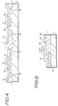
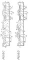
- FIGS.5A through 5D a description will be given of a first conceivable method of producing a semiconductor device, by referring to FIGS.5A through 5D.
- FIGS.5A through 5D those parts which are essentially the same as those corresponding parts in FIGS.1A through 1K, 2A through 2C, 3 and 4 are designated by the same reference numerals, and a description thereof will be omitted.
- This method produces a first embodiment of semiconductor device.
- the steps described in conjunction with FIGS.1A through 1C and 4 are carried out to form the SiO 2 layer 52 as shown in FIG.4.
- a part 52A of the SiO 2 layer 52 corresponding to the peripheral circuit is removed by an RIE so that only a part 52B of the SiO 2 layer 52 remains.
- side wall SiO 2 layers 57 and 58 are formed at the side wall portions of the gate electrode 31.
- an nMOS FET 60 which uses the n - -type diffusion layer 36 as the n - -type source diffusion layer and the n - -type diffusion layer 37 as the n - -type drain diffusion layer makes up the memory cell 3.
- the nMOS FET 23 has the LDD structure, but the nMOS FET 60 does not have the LDD structure because an undesirable current leak is introduced at the pn junction of the LDD structure. Such a current leak is generated due to a surface deterioration caused by the RIE which is carried out with respect to the p-type Si substrate 1. This current leak deteriorates the charge storage characteristic of the memory cell 3, and a transistor having the LDD structure is unsuitable for use as the transistor of the memory cell 3. On the other hand, such a current leak is negligible in the case of the transistor which is used for the peripheral circuit 4, as long as a satisfactory current driving capability is ensured. This is the reason why the nMOS FET 23 has the LDD structure while the nMOS FET 60 does not.
- a thermal oxidation is carried out to form a SiO 2 layer 59 having a thickness of 150 ⁇ , for example, on the exposed surface of the p-type Si substrate 1 and the exposed surface of the gate electrode 31 as shown in FIG.5B.
- the part 52B, the field oxide layer 2, the gate electrode 31 and the side wall SiO 2 layers 57 and 58 are used as a mask when implanting As ions into the p-type Si substrate 1 with an energy of 50 keV and a dosage of 4 x 10 15 cm -2 , for example, so as to form the n + -type source diffusion layer 26 and the n + -type drain diffusion layer 29.
- a resist mask may be used in place of the part 52B of the SiO 2 layer 52.
- the nMOS FET 23 having the source diffusion layer 24 which is made up of the n - -type source diffusion layer 25 and the n + -type source diffusion layer 26, and the drain diffusion layer 27 which is made up of the n - -type drain diffusion layer 28 and the n + -type drain diffusion layer 29 is formed.
- a contact hole 61 is formed in the part 52B above the n - -type drain diffusion layer 37.
- the polysilicon layer 46 having the thickness of 2000 ⁇ , for example, is formed on the entire surface of the stacked structure, and the resistance of this polysilicon layer 46 is reduced by carrying out an As ion implantation.
- the storage electrode 19 shown in FIG.5D is formed by patterning the polysilicon layer 46 by an RIE.
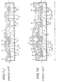
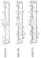
- FIGS.7A through 7K those parts which are essentially the same as those corresponding parts in FIGS.1A through 1K, 2A through 2C, 3, 4, 5A through 5D and 6 are designated by the same reference numerals, and a description thereof will be omitted.
- This embodiment of the method produces a semiconductor device according to the present invention.
- steps similar to those described in conjunction with FIGS.1A and 1B are carried out as shown in FIGS.7A and 7B.
- the p-type Si substrate 1 is prepared as shown in FIG.7A.
- the surface of this p-type Si substrate 1 is selectively oxidized to form the field oxide layer 2 which has a thickness of 5000 ⁇ , for example.
- the SiO 2 layers 13 and 30 are formed in the device region by a thermal oxidation to a thickness of 150 ⁇ , for example.
- the polysilicon layer 35 having a thickness of 2000 ⁇ , for example, is formed on the entire surface of the stacked structure by a CVD.
- the polysilicon layer 35 is patterned, and as shown in FIG.7B, the gate electrodes 14 and 31 are formed. Then, the gate electrodes 14 and 31 are used as a mask when implanting phosphorous (P) ions into the p-type Si substrate 1 with an energy of 50 keV and a dosage of 1 x 10 13 cm -2 , for example. As a result, the n - -type diffusion layers 36, 37, 38 and 39 are formed.
- P phosphorous
- the nMOS FET 60 makes up the memory cell 3, and this nMOS FET 60 uses the n - -type diffusion layer 36 as the n - -type source diffusion layer and the n - -type diffusion layer 37 as the n - -type drain diffusion layer.
- a part 64A of the SiO 2 layer 64 corresponding to the peripheral circuit is removed by an RIE so that only a part 64B of the SiO 2 layer 64 corresponding to the memory cell remains as shown in FIG.7D.
- the RIE is ended by making an endpoint detection which detects a change in a plasma light emission spectrum intensity when the surface of the p-type Si substrate 1 is exposed at the peripheral circuit.
- side wall SiO 2 layers 65 and 66 are formed at the side wall portions of the gate electrode 31.
- the endpoint detection described above is also used to detect the end of this RIE.
- Side wall SiO 2 layers 68, 69 and 70 are respectively formed at the side wall portions of the part 64B along the gate electrode 14 and at the side wall portion on the end of the part 64B.
- side wall SiO 2 layers 71 and 72 are respectively formed at the side wall portions of the side wall SiO 2 layers 65 and 66.
- a side wall SiO 2 layer 73 in which the side wall SiO 2 layers 65 and 71 are integrated, and a side wall SiO 2 layer 74 in which the side wall SiO 2 layers 66 and 72 are integrated are formed.
- a thermal oxidation is carried out to form a SiO 2 layer 75 having a thickness of 150 ⁇ , for example, on the exposed surfaces of the p-type Si substrate 1 and the gate electrode 31.
- the part 64B of the SiO 2 layer 64, the field oxide layer 2, the gate electrode 31 and the side wall SiO 2 layers 73 and 74 are used as a mask when implanting As ions into the p-type Si substrate 1 with an energy of 50 keV and a dosage of 4 x 10 15 cm -2 , for example, so as to form the source diffusion layer 24 which is made up of the n - -type source diffusion layer 25 and the n + -type source diffusion layer 26 and the drain diffusion layer 27 which is made up of the n - -type drain diffusion layer 28 and the n + -type drain diffusion layer 29.
- a resist mask may be used at the memory cell.
- an oxidation process may be made after the step shown in FIG.7D and the As + ion implantation may be
- the nMOS FET 23 which has the source diffusion layer 24 and the drain diffusion layer 27 is formed.
- the polysilicon layer 46 is patterned as shown in FIG.7I, and the storage electrode 19 is formed.
- This storage electrode 19 makes an ohmic contact with the n + -type drain diffusion layer 11 via the contact hole 77.
- a natural oxide layer which is formed at the exposed surface of the storage electrode 19 is removed by an etching using the HF solution.
- a thermal oxidation is carried out to form the SiO 2 capacitor insulator layer 20 which has a thickness of 100 ⁇ , for example, on the exposed surface of the storage electrode 19 as shown in FIG.7J.
- the polysilicon layer 47 having a thickness of 2000 ⁇ , for example, is formed on the entire surface of the stacked structure as shown in FIG.7J, and P is thermally diffused into the polysilicon layer 47 to reduce the resistance.
- this polysilicon layer 47 is patterned to form the confronting electrode 21 as shown in FIG.7K.
- the PSG layer 16 is formed on the entire surface of the stacked structure to a thickness of 5000 ⁇ , for example, as shown in FIG.7K.
- the contact holes 18, 33 and 34 are formed in the PSG layer 16 as shown in FIG.7K, and the bit line 17 and the other interconnection 32 are formed. As a result, the second embodiment of the DRAM having the stacked capacitor 6 is obtained.
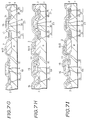
- the side wall SiO 2 layers 68, 69 and 70 are formed at the side wall portions of the part 64B of the SiO 2 layer 64 provided below the storage electrode 19 as shown in FIG.7F, so as to flatten the vertical stepped portion of the side wall portions.
- the polysilicon layer 46 is etched to form the storage electrode 19, it is possible to prevent the polysilicon from remaining at the side wall portion of the part 64B as shown in FIGS.7H and 7I.
- FIGS.7H and 7I As a result, it is possible to positively prevent the mutually adjacent storage electrodes 19 from being short-circuited by a remaining polysilicon piece, and the formation of the storage electrode 19 is facilitated.
- the surface of the n - -type drain diffusion layer 37 to which the storage electrode 19 connects is covered by the part 64B of the SiO 2 layer 64 as shown in FIG.7D.
- the surface of the n - -type drain diffusion layer 37 will not be subjected to the plasma atmosphere when the SiO 2 layer 67 is etched as may be understood from FIGS.7E and 7F.
- the surface of the n - -type drain diffusion layer 37 is positively protected from metal contamination.
- the side wall SiO 2 layer 69 above the n - -type drain diffusion layer 37 is formed via the part 64B of the SiO 2 layer 64.
- the stress at the tip end of the part 64B with respect to the p-type Si substrate 1 is reduced.
- the drain diffusion layer of the nMOS FET 60 is formed only from the n - -type drain diffusion layer 37 and no ion implantation of impurity needs to be made to form an n + -type drain diffusion layer, it is possible to prevent the generation of crystal defect such as the dislocation loop and the edge dislocation which occur during a recrystallization process after the ion implantation of the impurity at a high dosage. Accordingly, the charge storage characteristic of the memory cell 3 can be improved.
- the nMOS FET 23 which forms the peripheral circuit has the LDD structure and is provided with the n + -type source diffusion layer 26 and the n + -type drain diffusion layer 29.
- the resistances of the source diffusion layer 24 and the drain diffusion layer 27 can be made small. Therefore, it is possible to ensure a sufficient current driving capability as a transistor of the peripheral circuit 4.
- the storage electrode 19 it is possible to simultaneously achieve three goals.
- a first transistor forms the memory cell and a second transistor forms the peripheral circuit.
- the first transistor may form a sense amplifier of the semiconductor device.
- the present invention is applied to the DRAM having stacked capacitors.
- the present invention is similarly applicable to other semiconductor devices such as a static RAM.
Landscapes
- Engineering & Computer Science (AREA)
- Manufacturing & Machinery (AREA)
- Semiconductor Memories (AREA)
- Metal-Oxide And Bipolar Metal-Oxide Semiconductor Integrated Circuits (AREA)
- Insulated Gate Type Field-Effect Transistor (AREA)
Claims (17)
- Dispositif à semiconducteur comprenant : un substrat semiconducteur (1) ; un premier transistor (60) formé sur ledit substrat semiconducteur, ledit premier transistor ayant une première région de diffusion de source (37), une première région de diffusion de drain (36), et une première électrode de grille (14) montée sur le substrat et disposée entre lesdites premières régions de diffusion (36, 37), ladite première région de diffusion de source et ladite première région de diffusion de drain étant formées dans ledit substrat semiconducteur ; un deuxième transistor (23) formé sur ledit substrat semiconducteur et adjacent au premier transistor, ledit deuxième transistor ayant une deuxième région de diffusion de source (24), une deuxième région de diffusion de drain (27), et une deuxième électrode de grille (31) montée sur le substrat et disposée entre lesdites deuxièmes régions de diffusion (24, 27), ladite deuxième région de diffusion de source et ladite deuxième région de diffusion de drain étant formées dans ledit substrat semiconducteur ; et une couche d'oxyde de grille (2) formée sur ledit substrat semiconducteur entre les premier et deuxième transistors (60, 23) afin d'isoler lesdits premier et deuxième transistors, caractérisé en ce qu'il est prévu :une première couche d'isolant (64B, 65, 66) qui couvre la surface dudit substrat semiconducteur (1), de façon que ladite première couche d'isolant couvre toute la surface du premier transistor (60) et les parties parois latérales de la deuxième électrode de grille (31) du deuxième transistor (23);une couche isolante de paroi latérale (68-72) étant formée sur ladite première couche d'isolant au niveau des parties parois latérales de la première électrode de grille (14), au niveau de la région de bord de la première couche d'isolant (64B), et au niveau des parties parois latérales de la deuxième électrode de grille; etune deuxième couche d'isolant (76) formée sur lesdits premier et deuxième transistors (60, 23), sur la couche d'isolation de paroi latérale (68-72), lesdites première et deuxième couches d'isolant (64B, 76) étant dotées de trous de contact destinés à des régions bornes des transistors (60, 23).
- Dispositif à semiconducteur selon la revendication 1, caractérisé en ce que ledit deuxième transistor (23) possède une structure à drain légèrement dopé (LDD).
- Dispositif à semiconducteur selon la revendication 1 ou 2, caractérisé en ce que ledit substrat semiconducteur (1) est d'un premier type semiconducteur, ladite première région de diffusion de source (36) et la première région de diffusion de drain (37) dudit premier transistor (60) sont dopées à un deuxième type semiconducteur selon un premier dosage, ladite deuxième région de diffusion de source (24) dudit deuxième transistor (23) comporte une première couche de diffusion de source (25) dopée au deuxième type semiconducteur selon un deuxième dosage et une deuxième couche de diffusion de source (26) dopée au deuxième type semiconducteur selon un troisième dosage, et ladite deuxième région de diffusion de drain (27) dudit deuxième transistor comporte une première couche de diffusion de drain (28) dopé au deuxième type semiconducteur selon le deuxième dosage et une deuxième couche de diffusion de drain (29) dopé au deuxième type semiconducteur selon le troisième dosage, lesdits premier et deuxième types semiconducteurs étant des types semiconducteurs différents, lesdits premier et deuxième dosages étant inférieurs audit troisième dosages.
- Dispositif à semiconducteur selon la revendication 3, caractérisé en ce que lesdits premier et deuxième types semiconducteurs sont respectivement les semiconducteurs de type p et n, et lesdits premier et deuxième transistors (60, 23) sont des transistors à effet de champ du type à grille isolée à canal n.
- Dispositif à semiconducteur selon l'une quelconque des revendications 1 à 4, caractérisé en ce que ledit premier transistor (60) forme une cellule de mémoire (3) d'un dispositif de mémoire à semiconducteur et ledit deuxième transistor (23) forme un circuit périphérique (4) du dispositif de mémoire à semiconducteur.
- Dispositif à semiconducteur selon la revendication 5, caractérisé en ce qu'il est en outre prévu un condensateur empilé (6) formé sur ladite deuxième couche d'isolant (76) et couplé audit premier transistor (60) afin de former la cellule de mémoire (3) du dispositif de mémoire à semiconducteur, et un trou de contact (77) formé dans lesdites première et deuxième couches d'isolant (64B, 76), ledit condensateur empilé établissant un contact avec ladite première région de diffusion de drain (37) via ledit trou de contact.
- Dispositif à semiconducteur selon l'une quelconque des revendications 1 à 6, caractérisé en ce que lesdites première et deuxième couches d'isolant (64B, 76) sont constituées en dioxyde de silicium.
- Procédé de production d'un dispositif à semiconducteur comprenant deux transistors adjacents sur un substrat semiconducteur (1) ayant une couche d'oxyde de champ (2) placée entre les deux transistors, le procédé comprenant les opérations suivantes :former une première grille (14) d'un premier transistor (60) et une deuxième grille (31) d'un deuxième transistor (23) sur le substrat semiconducteur (1) ayant la couche d'oxyde de champ (2) pour isoler lesdits premier et deuxième transistors ; etformer des régions de diffusion d'impureté (36, 37, 24, 27) dans ledit substrat semiconducteur afin de réaliser une première région de diffusion de source (36) et une première région de diffusion de drain (37) dudit premier transistor, les premières régions de diffusion (36, 37) étant disposées adjacentes de côtés opposés de la première grille (14), ainsi qu'une deuxième région de diffusion de source (24) et une deuxième région de diffusion de drain (27) dudit deuxième transistor, les deuxièmes régions de diffusion (24, 27) étant disposées adjacentes de côtés opposés de la deuxième grille (31), caractérisé en ce que sont prévues les opérations suivantes :former une première couche d'isolant (64B, 65, 66) qui couvre la surface dudit substrat semiconducteur (1) de façon que ladite première couche d'isolant (64B) couvre toute la surface du premier transistor (60) et les parties parois latérales de la deuxième grille (31) du deuxième transistor (23);former une couche d'isolation de paroi latérale (68-72) sur ladite première couche d'isolant(i) au niveau de parties parois latérales de la première grille (14) et à celui de la région de bord de la première couche d'isolant, et(ii) au niveau des parties parois latérales (73, 74) de ladite deuxième grille (31) dudit deuxième transistor (23),la couche d'isolation de paroi latérale (68-72) étant formée par exécution d'une gravure anisotrope relativement à une couche d'isolation initiale (67) qui couvre le substrat semiconducteur (1); etformer une deuxième couche d'isolant (75) qui couvre des surfaces exposées dudit substrat semiconducteur et de ladite deuxième grille dudit deuxième transistor,ladite opération de formation de la première couche d'isolant (64B, 65, 66) comportant les sous-opérations qui consistent à former ladite première couche d'isolant (64) sur toute la surface dudit substrat semiconducteur (1) y compris lesdites première et deuxième grilles (14, 31), et à retirer dudit deuxième transistor (23), par une gravure anisotrope, ladite première couche d'isolant (64A).
- Procédé selon la revendication 8, caractérisé en ce que ladite opération de formation de la deuxième couche d'isolant forme ladite deuxième couche d'isolant par une oxydation thermique.
- Procédé selon la revendication 8 ou 9, caractérisé en ce que ledit deuxième transistor (23) possède une structure à drain légèrement dopé (LDD).
- Procédé selon l'une quelconque des revendications 8 à 10, caractérisé en ce que ledit substrat semiconducteur (1) est d'un premier type semiconducteur, ladite opération de formation des régions de diffusion d'impureté dope lesdites première et deuxième régions de diffusion de source (36, 24) et lesdites première et deuxième régions de diffusion de drain (37, 27) desdits premier et deuxième transistors (60, 23) à un deuxième type semiconducteur avec un premier dosage, lesdits premier et deuxième types semiconducteurs étant des types semiconducteurs différents.
- Procédé selon la revendication 11, caractérisé en ce qu'il est en outre prévu l'opération consistant à doper une partie (26, 29) de chacune des régions que forment ladite deuxième région de diffusion de source (24) et ladite deuxième région de diffusion de drain (27) dudit deuxième transistor (23) au deuxième type semiconducteur avec un deuxième dosage, le premier dosage étant inférieur au deuxième dosage.
- Procédé selon la revendication 12, caractérisé en ce que lesdits premier et deuxième types semiconducteurs sont respectivement les semiconducteurs de type p et n, et lesdits premier et deuxième transistors (60, 23) sont des transistors à effet de champ du type à grille isolée à canal n.
- Procédé selon l'une quelconque des revendications 8 à 13, caractérisé en ce que ledit premier transistor (60) forme une cellule de mémoire (3) d'un dispositif de mémoire à semiconducteur et ledit deuxième transistor (23) forme un circuit périphérique (4) du dispositif de mémoire à semiconducteur.
- Procédé selon la revendication 14, caractérisé en ce que sont en outre prévues les opérations consistant à former un trou de contact (61) dans ladite première couche d'isolant (52B) et à former un condensateur empilé (6) sur ladite première couche d'isolant, ledit condensateur empilé ayant une électrode de stockage (19) qui établit un contact avec ladite première région de diffusion de drain (37) via ledit trou de contact afin de former la cellule de mémoire (3) du dispositif de mémoire à semiconducteur.
- Procédé selon l'une quelconque des revendications 8 à 15, caractérisé en ce que lesdites première et deuxième couches d'isolant (52B) sont constituées en dioxyde de silicium.
- Procédé selon la revendication 12, caractérisé en ce que ladite opération de dopage implante des ions d'impureté dans ladite deuxième région de diffusion de source (24) et ladite deuxième région de diffusion de drain (27) dudit deuxième transistor (23) en utilisant comme masque au moins ladite deuxième grille (31) ainsi que ladite première couche d'isolant (65, 66) et ladite couche d'isolation de paroi latérale (71, 72) se trouvant au niveau des parties parois latérales de ladite deuxième grille.
Applications Claiming Priority (2)
| Application Number | Priority Date | Filing Date | Title |
|---|---|---|---|
| JP1137861A JPH0821687B2 (ja) | 1989-05-31 | 1989-05-31 | 半導体装置及びその製造方法 |
| JP137861/89 | 1989-05-31 |
Publications (3)
| Publication Number | Publication Date |
|---|---|
| EP0401113A2 EP0401113A2 (fr) | 1990-12-05 |
| EP0401113A3 EP0401113A3 (fr) | 1992-07-29 |
| EP0401113B1 true EP0401113B1 (fr) | 1996-07-24 |
Family
ID=15208471
Family Applications (1)
| Application Number | Title | Priority Date | Filing Date |
|---|---|---|---|
| EP90401446A Expired - Lifetime EP0401113B1 (fr) | 1989-05-31 | 1990-05-30 | Dispositif semi-conducteur et son procédé de fabrication |
Country Status (4)
| Country | Link |
|---|---|
| EP (1) | EP0401113B1 (fr) |
| JP (1) | JPH0821687B2 (fr) |
| KR (1) | KR930007524B1 (fr) |
| DE (1) | DE69027894T2 (fr) |
Families Citing this family (8)
| Publication number | Priority date | Publication date | Assignee | Title |
|---|---|---|---|---|
| DE4034169C2 (de) * | 1989-10-26 | 1994-05-19 | Mitsubishi Electric Corp | DRAM mit einem Speicherzellenfeld und Herstellungsverfahren dafür |
| JP2673385B2 (ja) * | 1989-10-26 | 1997-11-05 | 三菱電機株式会社 | 半導体装置 |
| IT1239707B (it) * | 1990-03-15 | 1993-11-15 | St Microelectrics Srl | Processo per la realizzazione di una cella di memoria rom a bassa capacita' di drain |
| KR940000510B1 (ko) * | 1991-03-20 | 1994-01-21 | 삼성전자 주식회사 | 반도체 메모리장치 및 그 제조방법 |
| KR940005802B1 (ko) * | 1991-07-09 | 1994-06-23 | 삼성전자 주식회사 | Cmos 반도체장치 및 그 제조방법 |
| EP0575688B1 (fr) * | 1992-06-26 | 1998-05-27 | STMicroelectronics S.r.l. | Programmation des cellules LDD-ROM |
| TW468273B (en) * | 1997-04-10 | 2001-12-11 | Hitachi Ltd | Semiconductor integrated circuit device and method for manufacturing the same |
| JP3061117B2 (ja) * | 1997-06-18 | 2000-07-10 | 日本電気株式会社 | 半導体装置の製造方法 |
Family Cites Families (5)
| Publication number | Priority date | Publication date | Assignee | Title |
|---|---|---|---|---|
| JPS61183952A (ja) * | 1985-02-09 | 1986-08-16 | Fujitsu Ltd | 半導体記憶装置及びその製造方法 |
| EP0218408A3 (fr) * | 1985-09-25 | 1988-05-25 | Hewlett-Packard Company | Procédé pour fabriquer une structure de drain faible dopée (LLD) dans des circuits intégrés |
| US4855801A (en) * | 1986-08-22 | 1989-08-08 | Siemens Aktiengesellschaft | Transistor varactor for dynamics semiconductor storage means |
| ATE97259T1 (de) * | 1986-10-16 | 1993-11-15 | Siemens Ag | Speicherzellenanordnung fuer dynamische halbleiterspeicher. |
| JPH01129440A (ja) * | 1987-11-14 | 1989-05-22 | Fujitsu Ltd | 半導体装置 |
-
1989
- 1989-05-31 JP JP1137861A patent/JPH0821687B2/ja not_active Expired - Fee Related
-
1990
- 1990-05-30 DE DE69027894T patent/DE69027894T2/de not_active Expired - Fee Related
- 1990-05-30 EP EP90401446A patent/EP0401113B1/fr not_active Expired - Lifetime
- 1990-05-31 KR KR1019900008047A patent/KR930007524B1/ko not_active Expired - Fee Related
Also Published As
| Publication number | Publication date |
|---|---|
| DE69027894T2 (de) | 1996-12-12 |
| DE69027894D1 (de) | 1996-08-29 |
| JPH0821687B2 (ja) | 1996-03-04 |
| KR930007524B1 (ko) | 1993-08-12 |
| JPH033360A (ja) | 1991-01-09 |
| EP0401113A3 (fr) | 1992-07-29 |
| KR900019242A (ko) | 1990-12-24 |
| EP0401113A2 (fr) | 1990-12-05 |
Similar Documents
| Publication | Publication Date | Title |
|---|---|---|
| US6545327B2 (en) | Semiconductor device having different gate insulating films with different amount of carbon | |
| US6388296B1 (en) | CMOS self-aligned strapped interconnection | |
| US5886385A (en) | Semiconductor device and manufacturing method thereof | |
| EP0138978B1 (fr) | Procede de fabrication d'un dispositif a semiconducteur de petites dimensions | |
| US4566175A (en) | Method of making insulated gate field effect transistor with a lightly doped drain using oxide sidewall spacer and double implantations | |
| US6417534B2 (en) | Semiconductor device and method of fabricating the same | |
| EP0503904A2 (fr) | Structure de contact d'une couche d'interconnexion placée sur une surface ayant des marches et SRAM ayant des interconnexions multicouches ainsi que son procédé de fabrication | |
| US5348897A (en) | Transistor fabrication methods using overlapping masks | |
| US5648673A (en) | Semiconductor device having metal silicide film on impurity diffused layer or conductive layer | |
| KR930010087B1 (ko) | 반도체 장치 및 그의 제조방법 | |
| US5460983A (en) | Method for forming isolated intra-polycrystalline silicon structures | |
| US7332388B2 (en) | Method to simultaneously form both fully silicided and partially silicided dual work function transistor gates during the manufacture of a semiconductor device, semiconductor devices, and systems including same | |
| US5438008A (en) | Method of making a semiconductor device having two transistors forming a memory cell and a peripheral circuit, wherein the impurity region of the first transistor is not subjected to an etching atmosphere | |
| KR20020001604A (ko) | 반도체 집적 회로 장치와 그 제조 방법 | |
| US5432105A (en) | Method for fabricating self-aligned polysilicon contacts on FET source/drain areas | |
| US5225357A (en) | Low P+ contact resistance formation by double implant | |
| US5497022A (en) | Semiconductor device and a method of manufacturing thereof | |
| EP0401113A2 (fr) | Dispositif semi-conducteur et son procédé de fabrication | |
| US5320976A (en) | Method for manufacturing VLSI semiconductor device | |
| US5705418A (en) | Process for fabricating reduced-thickness high-resistance load resistors in four-transistor SRAM devices | |
| US5686338A (en) | Process for fabricating high-resistance load resistors using dummy polysilicon in four-transistor SRAM devices | |
| JP3324648B2 (ja) | 半導体装置の製造方法 | |
| US5851873A (en) | Method of making semiconductor memory device | |
| EP0445756B1 (fr) | Transitor MOS à haute tension et procédé de fabrication et dispositif à semi-conducteur avec un transistor MOS à haute tension et procédé de fabrication | |
| US5959334A (en) | Semiconductor memory device |
Legal Events
| Date | Code | Title | Description |
|---|---|---|---|
| PUAI | Public reference made under article 153(3) epc to a published international application that has entered the european phase |
Free format text: ORIGINAL CODE: 0009012 |
|
| AK | Designated contracting states |
Kind code of ref document: A2 Designated state(s): DE FR GB |
|
| PUAL | Search report despatched |
Free format text: ORIGINAL CODE: 0009013 |
|
| AK | Designated contracting states |
Kind code of ref document: A3 Designated state(s): DE FR GB |
|
| 17P | Request for examination filed |
Effective date: 19921009 |
|
| 17Q | First examination report despatched |
Effective date: 19940803 |
|
| GRAH | Despatch of communication of intention to grant a patent |
Free format text: ORIGINAL CODE: EPIDOS IGRA |
|
| GRAH | Despatch of communication of intention to grant a patent |
Free format text: ORIGINAL CODE: EPIDOS IGRA |
|
| GRAA | (expected) grant |
Free format text: ORIGINAL CODE: 0009210 |
|
| AK | Designated contracting states |
Kind code of ref document: B1 Designated state(s): DE FR GB |
|
| REF | Corresponds to: |
Ref document number: 69027894 Country of ref document: DE Date of ref document: 19960829 |
|
| ET | Fr: translation filed | ||
| PLBE | No opposition filed within time limit |
Free format text: ORIGINAL CODE: 0009261 |
|
| STAA | Information on the status of an ep patent application or granted ep patent |
Free format text: STATUS: NO OPPOSITION FILED WITHIN TIME LIMIT |
|
| 26N | No opposition filed | ||
| REG | Reference to a national code |
Ref country code: GB Ref legal event code: IF02 |
|
| PGFP | Annual fee paid to national office [announced via postgrant information from national office to epo] |
Ref country code: FR Payment date: 20050511 Year of fee payment: 16 |
|
| PGFP | Annual fee paid to national office [announced via postgrant information from national office to epo] |
Ref country code: GB Payment date: 20050525 Year of fee payment: 16 |
|
| PGFP | Annual fee paid to national office [announced via postgrant information from national office to epo] |
Ref country code: DE Payment date: 20050526 Year of fee payment: 16 |
|
| PG25 | Lapsed in a contracting state [announced via postgrant information from national office to epo] |
Ref country code: GB Free format text: LAPSE BECAUSE OF NON-PAYMENT OF DUE FEES Effective date: 20060530 |
|
| PG25 | Lapsed in a contracting state [announced via postgrant information from national office to epo] |
Ref country code: DE Free format text: LAPSE BECAUSE OF NON-PAYMENT OF DUE FEES Effective date: 20061201 |
|
| GBPC | Gb: european patent ceased through non-payment of renewal fee |
Effective date: 20060530 |
|
| REG | Reference to a national code |
Ref country code: FR Ref legal event code: ST Effective date: 20070131 |
|
| PG25 | Lapsed in a contracting state [announced via postgrant information from national office to epo] |
Ref country code: FR Free format text: LAPSE BECAUSE OF NON-PAYMENT OF DUE FEES Effective date: 20060531 |