EP0402742A2 - Rauschformungsrequantisierungsschaltkreis - Google Patents
Rauschformungsrequantisierungsschaltkreis Download PDFInfo
- Publication number
- EP0402742A2 EP0402742A2 EP90110647A EP90110647A EP0402742A2 EP 0402742 A2 EP0402742 A2 EP 0402742A2 EP 90110647 A EP90110647 A EP 90110647A EP 90110647 A EP90110647 A EP 90110647A EP 0402742 A2 EP0402742 A2 EP 0402742A2
- Authority
- EP
- European Patent Office
- Prior art keywords
- signal
- requantization
- circuit
- noise shaping
- digital signal
- Prior art date
- Legal status (The legal status is an assumption and is not a legal conclusion. Google has not performed a legal analysis and makes no representation as to the accuracy of the status listed.)
- Granted
Links
Images


Classifications
-
- H—ELECTRICITY
- H03—ELECTRONIC CIRCUITRY
- H03M—CODING; DECODING; CODE CONVERSION IN GENERAL
- H03M1/00—Analogue/digital conversion; Digital/analogue conversion
- H03M1/66—Digital/analogue converters
-
- H—ELECTRICITY
- H03—ELECTRONIC CIRCUITRY
- H03M—CODING; DECODING; CODE CONVERSION IN GENERAL
- H03M7/00—Conversion of a code where information is represented by a given sequence or number of digits to a code where the same, similar or subset of information is represented by a different sequence or number of digits
- H03M7/30—Compression; Expansion; Suppression of unnecessary data, e.g. redundancy reduction
- H03M7/3002—Conversion to or from differential modulation
- H03M7/3004—Digital delta-sigma modulation
- H03M7/3015—Structural details of digital delta-sigma modulators
- H03M7/3031—Structural details of digital delta-sigma modulators characterised by the order of the loop filter, e.g. having a first order loop filter in the feedforward path
- H03M7/3042—Structural details of digital delta-sigma modulators characterised by the order of the loop filter, e.g. having a first order loop filter in the feedforward path the modulator being of the error feedback type, i.e. having loop filter stages in the feedback path only
-
- H—ELECTRICITY
- H03—ELECTRONIC CIRCUITRY
- H03M—CODING; DECODING; CODE CONVERSION IN GENERAL
- H03M7/00—Conversion of a code where information is represented by a given sequence or number of digits to a code where the same, similar or subset of information is represented by a different sequence or number of digits
- H03M7/30—Compression; Expansion; Suppression of unnecessary data, e.g. redundancy reduction
- H03M7/3002—Conversion to or from differential modulation
- H03M7/3004—Digital delta-sigma modulation
- H03M7/3015—Structural details of digital delta-sigma modulators
- H03M7/302—Structural details of digital delta-sigma modulators characterised by the number of quantisers and their type and resolution
- H03M7/3024—Structural details of digital delta-sigma modulators characterised by the number of quantisers and their type and resolution having one quantiser only
- H03M7/3028—Structural details of digital delta-sigma modulators characterised by the number of quantisers and their type and resolution having one quantiser only the quantiser being a single bit one
Definitions
- the present invention relates to a noise shaping requantization circuit for use in converting a digital signal to an analog signal by employing a low resolution digital/analog converter.
- a requantization circuit functions by requantizing the digital signal to convert it to a digital signal having a lower degree of resolution, with the requantization being executed such that the frequency distribution of the resampling noise that is generated in the requantization process is shaped such as to shift the noise components to a high frequency range, thereby effectively increasing the signal-to-noise ratio of the output digital signal.
- Noise shaping quantization methods for use in achieving a high accuracy of D/A conversion operation are now well known, whereby an input digital signal (originally generated by sampling of an analog signal at an original sampling frequency which is higher than the minimum, i.e. Nyqyuist sampling frequency) is resampled and requantized using a resampling frequency that is substantially higher than the original sampling frequency (i.e. oversampling is executed) and using a requantization step size that is substantially larger than the original quantization step size of the input digital signal (i.e. a lower degree of resolution is used than that used to derive the original digital signal).
- a D/A converter based on such a noise shaping requantization circuit is used in two basic types of application, i.e. for D/A conversion or for A/D conversion.
- D/A conversion an original input digital signal is resampled as described above, and the resultant requantized output digital signal is supplied to a D/A conversion section, to be converted to analog form.
- A/D conversion an original analog signal is sampled at an original sampling frequency (i.e.
- the resultant output digital signal is then inputted to an internal noise shaping requantization circuit, to obtain a requantized digital signal which is then transferred through an internal D/A conversion section to obtain an analog signal which is fed back to the input such as to form a negative feedback loop.
- the accuracy of the output digital signal is thereby increased.
- the oversampling technique enables the internal configuration to be made very simple, since the internal D/A conversion can have a very low degree of resolution (e.g. with a total of only two or three quantization steps). This serves to eliminate any problems of linearity errors in the internal D/A conversion, and makes it unnecessary to perform adjustment or trimming of the circuit.
- such a configuration can readily be adapted to implementation in integrated circuit form.
- a simple digital/analog converter section having low resolution but a very high degree of linearity such as a PWM (pulse width modulation) type of digital/analog converter circuit can be used to convert the requantized digital signal to analog form with a very high degree of accuracy.
- PWM pulse width modulation
- Fig. 1A is a block diagram of a prior art noise shaping requantization circuit (referred to in the following simply as a requantization circuit), which utilizes a method of requantization that is a development of the delta-sigma method.
- the circuit of Fig. 1A provides a fourth order noise shaping characteristic.
- numeral 5 denotes an input terminal of an input digital signal X(z)
- 7 denotes a requantizer for converting the input digital signal to an output signal Y′(z) having a lower degree of resolution than the input digital signal
- 6 denotes an output terminal for transferring an output signal produced from the requantizer
- 8 to 11 denote subtractors
- 12 to 15 denote adders
- 16 to 20 denote delay elements each of which provides a unit delay that is equal to one resampling period.
- the requantization circuit of Fig. 1A provides a fourth order noise shaping characteristic as stated above. However if subtractor 11, adder 15 and delay element 20 in Fig. 1A are removed, and the output signal from the adder 14 applied directly to the requantizer 7, then the circuit will provide a third order noise shaping characteristic.
- Such a prior art requantization circuit for providing a third order noise shaping characteristic is shown in Fig. 1B, and will be referred to in the following as the prior art example No. 1.
- the requantization circuit of Fig. 1A which provides a fourth order noise shaping characteristic, will be referred to in the following as the prior art example No. 2.
- the input signal A′(z) of the requantizer 7 and the output signal Y′(z) from the requantization circuit, given by the equations (1) and (2) above, can be expressed by the following equations (3) and (4) respectively:
- A′(z) X(z) + ⁇ (1 - z ⁇ 1) K - 1 ⁇ . N(z) (3)
- Y′(z) X(z) + (1 - z ⁇ 1) K . N(z) (4)
- the term ((1 - z ⁇ 1)) K provides a differential characteristic, whereby gain varies in proportion to frequency such that the amplitude of the quantization error (quantization noise) components of the output signal expressed by equation (4) will be reduced in accordance with lowering of frequency. That is to say, the desired noise shaping characteristic is exhibited.
- the factor K in the above equations expresses the order of the noise shaping circuit..
- the requantization circuit of the prior art example No. 1 exhibits a third order noise shaping characteristic
- the requantization circuit of the prior art example No. 2 exhibits a fourth order noise shaping characteristic
- the above relationship (6) signifies that the limits of the input signal A′(z) of the requantizer 7 are widened with respect to the limits of the input signal X(z), by the amount ⁇ (2 K - 1).P, and hence, the higher is the order K, the greater will become the level of the input signal A′(z) of the requantizer 7, and hence, the greater will become the necessary number of output steps of the requantizer 7 (i.e. the higher will become the necessary degree of resolution).
- the limits of the input signal A′(z) of the requantizer 7 are wider than the limits of the input digital signal by the amount ⁇ 7P, in the case of the prior art example No.
- the noise shaping requantization circuit for converting an input digital signal having a high degree of resolution to a requantized output digital signal having a lower degree of resolution, using a resampling frequency that is higher than an original sampling frequency of the input digital signal, which is characterized in that, designating the input digital signal as X(z), the requantized output signal as Y(z), and the unit delay time corresponding to the resampling period as z ⁇ 1, the noise shaping requantization circuit comprises an operational circuit which receives the input digital signal X(z) and the requantized output signal Y(z) and generates an output signal which is expressed by the following: where the respective constants b, c, d and e simultaneously satisfy all of the following relationships: b ⁇ 1/2, e ⁇ 0, d + e > 0 b(d + e) (c + d + e) - b2
- Such a noise shaping requantization circuit converts an input digital signal having high resolution into a requantized output signal having a lower degree of resolution, by using a resampling frequency that is higher than the original sampling frequency of that input digital signal, and provides a substantially improved performance by comparison with prior art types of noise-shaping requantization circuit.
- the noise shaping requantization circuit of the present invention can function with a substantially lower degree of output resolution than the prior art noise shaping requantization circuit. That is to say, a larger requantization step size can be utilized with the noise shaping requantization circuit of the present invention, which is basically advantageous as described hereinabove.
- noise shaping requantization circuit according to the present invention and a prior art type of noise shaping requantization circuit are configured such as to operate with an identical value of output resolution (requantization step size), then the noise shaping requantization circuit of the present invention will provide a substantially greater degree of S/N improvement than the prior art circuit.
- Fig. 2 is a block diagram showing the general configuration of a noise shaping requantization circuit according ot the present invention, for converting an input digital signal having a high degree of resolution to a requantized output digital signal having a lower degree of resolution, by using a resampling frequency that is higher than the original sampling frequency of the input digital signal.
- Numeral 1 denotes an input digital signal input terminal
- 2 denotes a noise shaping requantization circuit output terminal
- 3 denotes an operational circuit
- 4 denotes a requantizer. Specific examples of configurations of the operational circuit 3 are shown in Figs. 4 to 9 and will be described in detail hereinafter.
- an input digital signal X(z) applied to the input terminal 1 is inputted to the operational circuit 3, as is also a requantized output digital signal Y(z) which is outputted from the requantizer 4.
- the operation circuit 3 operates on these input signals such as to produce an output digital signal A(z), which is expressed as where the respective constants b, c, d and e simultaneously satisfy all of the following relationships b ⁇ 1/2, e ⁇ 0, d + e > 0 (7) b(d + e) (c + d + e) - b2e - 1.2(d + e)2 > 0 (8) 8b + 4c + 2d + e ⁇ 15 (9) 8b + 4c + 2d ⁇ 14 + e (10)
- the requantizer 4 converts the output signal A(z) produced from the operational circuit 3 to the requantized output signal Y(z), which has a lower degree of resolution, and supplies the requantized output digital signal Y(z) to the output terminal 2.
- G(z) expresses a recursive type of transfer characteristic.
- T designating T as the resampling period
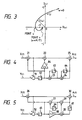
- the limits of the value ⁇ can be expressed as a vector path which is traced out by G(j ⁇ ), as shown in Fig. 3.
- the vector path in the range ⁇ /T ⁇ ⁇ ⁇ 2 ⁇ /T is obtained by folding over the vector path in the range 0 ⁇ ⁇ /T about the real axis.
- the vector path in the range 2c ⁇ /T ⁇ ⁇ ⁇ 2(k+1) ⁇ /T, where T is a natural number is obtained by folding over the vector path in the range 0 ⁇ 2c/T.
- the control system will be stable if the point u lies on the real axis at a position which is more negative than -1, and if the point v lies on the real axis at a point which is more positive than -1, i.e. if there is a boundary point at the left side of the vector path, as increases.
- e 0 , then from the relationships (10) and (33) the following are obtained: Mf
- e 0 ⁇ 7 (35)
- a noise shaping requantization circuit is configured to provide a fourth order noise shaping characteristic, as for the prior art example No. 2, by setting the value e > 1/2, then designating the value of Mf that is obtained in this case as Mf
- the value of Mf is smaller than that which can be achieved with the previously described prior art examples. That is to say, a greater margin of stability (as determined by the position of the point v) is obtained than is possible with the prior art examples.
- condition b ⁇ 1/2 that is given by the relationship (7) above for as precondition of the present invention will be discussed.
- the necessary condition for stability of a control system is that b > 0, and also the conditions given by relationships (7), i.e. e ⁇ 0 , (d + e) > 0, and the relationships (27) and (28) must each be satisfied to ensure stability.
- the condition is also set that b ⁇ 1/2.
- a noise shaping requantization circuit satisfies the relationships (7), (8), (9) and (10) and provides a sufficiently high degree of stability in practical operation.
- U(j ⁇ ) can be expressed by the following equation (43): U(j ⁇ ) ⁇ e + j(d - e) ⁇ T (43)
- T (which is extremely small value, close to zero as stated above)
- ⁇ is a positive constant
- K is a natural number
- the maximum signal-to-noise ratio within the signal frequency range will now be derived for requantization as expressed by the equations (55) and (56).
- Designating the requantization frequency as ⁇ a the upper limit of the signal frequency range as the Nyquist frequency for the original sampling signal (i.e. ⁇ s /2), the output step size of the requantizer as ⁇ , then the requantized output signal Y(z) is distributed uniformly within the limits ⁇ ⁇ /2. In the frequency domain, gain G is uniform (i.e. has the requisite white noise characteristic).
- Designating the power spectrum density as ⁇ o the maximum positive value of the input digital signal X(z) will be designated as L . ⁇ /2, so that the maximum sine wave signal power Sp is obtained as:
- the requantization noise power Np within the signal frequency range is obtained as:
- the spectral density ⁇ o can be obtained from the equations (60), (61) as:
- the degree of signal-to-noise ratio improvement can be expressed in units of dB, as follows:
- the values of the constants b, c, d and e have an effect only upon the requantization noise (N(z) or N(j ⁇ )) components, and do not have any effect upon the signal components (i.e. X(z) or X(j ⁇ )). That is to say, the values of the constants b, c, d and e have no effect at all on the frequency characteristics, gain, etc. of the signal components, and hence any effects on these can be ignored when selecting the respective values for the constants b, c, d and e.
- Equation (79) The value that is provided by equation (79) must be used in conjunction with the level of the signal X(z) in order to determine the absolute value of the requantizer input signal amplitude range. Since the range of the input signal applied to the requantizer is: ⁇ (
- a quantitative analysis of the prior art example number 1 and prior art example No. 2 respectively can be executed by setting the values set out in equations (82), (83) above respectively into the equations that have been used for quantitative analysis of a noise shaping requantization circuit according to the present invention hereinabove.
- Table 1 shows computed values for each of 7 representative embodiments of the present invention, based on the operational circuit configurations of Figs. 4 to 9, with respective values for the constants b, c, d and e, values for degree of signal-to-noise ratio improvement4 (in units of dB), values for Mp and Mf, and various other characteristics values described hereinabove.
- Table 2 similarly shows respective values for the constants b, c, d and e, values for degree of signal-to-noise ratio improvement (in units of dB), values for Mp and Mf, and various other characteristic values described hereinabove, as for Table 1, for the prior art example No. 1 and prior art example No. 2.
- the values for are, respectively, the sum totals of the absolute values of the coefficients a i (i.e. the coefficients for z ⁇ 1 N(z) as defined in equation (73) given hereinabove), for sets of values of i respectively extending from 1 to 4, from 1 to 8, and from 1 to infinity.
- [A - X] max 1 and [A - X] max 2 are the respective values of input signal amplitude range for the requantizer, as expressed by equations (79) and (80) respectively,and the required degree of resolution can be obtained from these.
- Each of these values in the tables is that by which the value P (i.e. 1/2 of the step size 2P) is multiplied to obtain the input signal amplitude range of the quantizer.
- each of the values of Mp and [A - X] max that are provided by these embodiments of the present invention will be respectively smaller than the values of Mp and [A - X] max that are provided by the prior art example No. 1. This is due to the fact that with these embodiments 1 and 2 of the present invention, a higher degree of stability and a lower requisite degree of output resolution are achieved, by comparison with the prior art example No. 1.
- embodiment 3 of the present invention and the prior art example No. 2 are each configured to provide an identical degree of signal-to-noise ratio improvement, then that embodiment of the present invention will be able to function with a lower degree of output resolution than the prior art example No. 2. Specifically, that embodiment of the present invention will be capable of operation with a degree of output resolution that is greater than the necessary output resolution of the prior art example 1 (having a third order noise shaping characteristic) by approximately ⁇ 1P. It can thus be understood that the embodiment 3 of the present invention can provide a fourth order noise shaping characteristic, while being capable of operating with a degree of output resolution that is substantially identical to that required by a conventional third order noise shaping requantization circuit.
- Each of the embodiments 4 to 6 of the present invention can function with a lower value of output resolution than the prior art example 1, while providing a degree of signal-to-noise ratio improvement that is less than that provided by the prior art example No. 2 by only approximately 6 dB.
- Determination of values for the constants b, c, d and e which will make Mp become small can be done by drawing a gain-phase characteristic diagram for a single-recursion transfer characteristic ⁇ equation (17) ⁇ within the range 0 ⁇ ⁇ ⁇ ⁇ , on a Nichols chart.
- Figs. 4 to 9 show specific configurations for the operational circuit 3, which are applicable to the representative embodiments 1 to 7 of a noise shaping requantization circuit according to the present invention.
- numerals 21 to 50 denote adders, 51 to 61 denote subtractors, 62 to 83 denote delay elements each providing a unit delay that is equal to the resampling period T.
- factor multipliers which use a factor value of 1/4.
- Each of these can be implemented in practice as an element which executes a 2-bit shift towards the LSB (lowest significance bit) direction, then replaces the two highest-significance bits by the value of the MSB (most significant bit) prior to executing that shift.
- 88 to 93 denote factor multipliers which use a factor value of 1/2.
- Each of these can be implemented in practice as an element which executes a 1-bit shift towards the LSB direction, then replaces the MSB of the result by the value of the MSB prior to executing that shift.
- Numerals 94 to 98 denote factor multipliers which use a factor value of 2.
- Each of these can be implemented in practice as an element which executes a 1-bit shift in the MSB direction.
- the output signal A(z) from the operational circuit shown in Fig. 4 can be expressed as:
- the noise shaping requantization circuit of embodiment 1 of the present invention uses the operational circuit that is shown in Fig. 4.
- the output signal A(z) from the operational circuit shown in Fig. 5 can be expressed as:
- the noise shaping requantization circuit of embodiment 2 of the present invention uses the operational circuit that is shown in Fig. 5.
- the output signal A(z) from the operational circuit shown in Fig. 6 can be expressed as:
- the noise shaping requantization circuit of embodiment 3 of the present invention uses the operational circuit that is shown in Fig. 6.
- the output signal A(z) from the operational circuit shown in Fig. 7 can be expressed as:
- the noise shaping requantization circuit of embodiment 4 of the present invention uses the operational circuit that is shown in Fig. 7.
- the output signal A(z) from the operational circuit shown in Fig. 8 can be expressed as:
- the noise shaping requantization circuit of embodiment 5 of the present invention uses the operational circuit that is shown in Fig. 8.
- the output signal A(z) can be expressed as follows:
- the output signal A(z) from the operational circuit shown in Fig. 9 can be expressed as:
- the noise shaping requantization circuit of embodiment 7 of the present invention (whose characteristic values are given in column 7 of Table 1) uses the operational circuit that is shown in Fig. 9.
- the present invention is not limited to a noise shaping requantization circuit which uses the typical embodiments of an operational circuit according to the present invention described above, and that it would be possible to use an operational circuit configuration other than those shown in Figs. 4 to 9 in such a noise shaping requantization circuit. It should also be noted that a noise shaping requantization circuit according to the present invention is not limited to the embodiment 1 to 7 described hereinabove, and that it would be possible to use other values for the respective constants b, c, d and e.
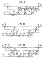
- Figs. 10 and 11 show two further embodiments of an operational circuit for a noise shaping requantization circuit according to the present invention.
- 100 to 105 denote respective adders
- 106 to 111 denote respective subtractors
- 112 to 119 denote delay elements
- 120 to 123 denote coefficient multipliers each of which multiplies by a factor 2.
- 124 and 125 are coefficient multipliers each of which multiplies by a factor "a", which can have a value such as 1/2 or 1/4, etc.
- the circuit of Fig. 11 is derived from that of Fig. 10 by eliminating the delay element 112 of Fig. 10 and inserting a delay element 116 at the output from the adder 103, and by eliminating the delay element 115 and inserting a delay element 119 at the output of the subtractor 111.
- the present invention comprises a noise shaping requantization circuit for executing requantization of an input digital signal having a high degree of resolution, using a requantization frequency which is substantially higher than the original requantization frequency of that input digital signal, to thereby convert the input digital signal to a requantized output digital signal having a lower degree of resolution than the input digital signal.
- a noise shaping requantization circuit which provides the same degree of signal-to-noise ratio improvement (with respect to a circuit which does not employ noise shaping requantization)
- a noise shaping requantization circuit according to the present invention can utilize a lower degree of output resolution (i.e. a greater magnitude of quantization step size).
- a noise shaping requantization circuit according to the present invention can provide a greater degree of signal-to-noise ratio improvement.
Landscapes
- Engineering & Computer Science (AREA)
- Theoretical Computer Science (AREA)
- Analogue/Digital Conversion (AREA)
- Compression, Expansion, Code Conversion, And Decoders (AREA)
Applications Claiming Priority (2)
| Application Number | Priority Date | Filing Date | Title |
|---|---|---|---|
| JP142346/89 | 1989-06-05 | ||
| JP1142346A JPH07109991B2 (ja) | 1989-06-05 | 1989-06-05 | ノイズシェーピング型再量子化回路 |
Publications (3)
| Publication Number | Publication Date |
|---|---|
| EP0402742A2 true EP0402742A2 (de) | 1990-12-19 |
| EP0402742A3 EP0402742A3 (de) | 1992-09-02 |
| EP0402742B1 EP0402742B1 (de) | 1996-05-08 |
Family
ID=15313229
Family Applications (1)
| Application Number | Title | Priority Date | Filing Date |
|---|---|---|---|
| EP90110647A Expired - Lifetime EP0402742B1 (de) | 1989-06-05 | 1990-06-05 | Rauschformungsrequantisierungsschaltkreis |
Country Status (5)
| Country | Link |
|---|---|
| US (1) | US5027119A (de) |
| EP (1) | EP0402742B1 (de) |
| JP (1) | JPH07109991B2 (de) |
| KR (1) | KR940003197B1 (de) |
| DE (1) | DE69026865T2 (de) |
Cited By (1)
| Publication number | Priority date | Publication date | Assignee | Title |
|---|---|---|---|---|
| DE10051153A1 (de) * | 2000-10-16 | 2002-04-25 | Accuride Int Gmbh | Gargutträgersystem für einen Backofen |
Families Citing this family (10)
| Publication number | Priority date | Publication date | Assignee | Title |
|---|---|---|---|---|
| JPH07109991B2 (ja) | 1989-06-05 | 1995-11-22 | 日本ビクター株式会社 | ノイズシェーピング型再量子化回路 |
| US5124703A (en) * | 1990-04-05 | 1992-06-23 | Matsushita Electric Industrial Co., Ltd. | Digital signal requantizing circuit using multistage noise shaping |
| US5736950A (en) * | 1995-01-31 | 1998-04-07 | The United States Of America As Represented By The Secretary Of The Navy | Sigma-delta modulator with tunable signal passband |
| DE19509117C2 (de) * | 1995-03-17 | 1997-02-27 | Bosch Gmbh Robert | Verfahren zur Überwachung der Übertragungsqualität digitalisierter Signale |
| EA002110B1 (ru) | 1996-03-28 | 2001-12-24 | ТЕКСАС ИНСТРУМЕНТС, КОПЕНГАГЕН АпС | Преобразование сигнала с импульсно-кодовой модуляцией в сигнал с широтно-импульсной модуляцией с равномерным распределением |
| US6373417B1 (en) * | 1999-02-23 | 2002-04-16 | Cirrus Logic, Inc. | Digital to analog converter using level and timing control signals to cancel noise |
| US6816100B1 (en) * | 1999-03-12 | 2004-11-09 | The Regents Of The University Of California | Analog-to-digital converters with common-mode rejection dynamic element matching, including as used in delta-sigma modulators |
| US6404369B1 (en) * | 2000-09-29 | 2002-06-11 | Teradyne, Inc. | Digital to analog converter employing sigma-delta loop and feedback DAC model |
| DE102005041917A1 (de) * | 2005-09-03 | 2007-03-08 | Schaeffler Kg | Tandemschrägkugellager |
| US9209791B2 (en) * | 2013-09-06 | 2015-12-08 | Texas Instruments Incorporated | Circuits and methods for cancelling nonlinear distortions in pulse width modulated sequences |
Family Cites Families (20)
| Publication number | Priority date | Publication date | Assignee | Title |
|---|---|---|---|---|
| FR2462062A1 (fr) * | 1979-07-20 | 1981-02-06 | Petit Jean P | Codeur delta sigma a double integration analogique et codeur delta sigma a double integration numerique |
| DE3021012C2 (de) * | 1980-06-03 | 1985-08-22 | ANT Nachrichtentechnik GmbH, 7150 Backnang | Verallgemeinertes interpolativers Verfahren zur Digital-Analog-Umsetzung von PCM Signalen |
| US4467291A (en) * | 1981-11-23 | 1984-08-21 | U.S. Philips Corporation | Delta modulator having optimized loop filter |
| US4453259A (en) * | 1982-04-20 | 1984-06-05 | Trw Inc. | Digital synchronization technique |
| DE3232558A1 (de) * | 1982-09-01 | 1984-03-01 | Siemens AG, 1000 Berlin und 8000 München | Digitaler dpcm-kodierer mit hoher verarbeitungsgeschwindigkeit |
| DE3232516A1 (de) * | 1982-09-01 | 1984-03-01 | Siemens AG, 1000 Berlin und 8000 München | Schneller dpcm-kodierer |
| CA1220867A (en) * | 1983-07-18 | 1987-04-21 | Northern Telecom Limited | Adaptive differential pcm system with residual-driven adaptation of feedback predictor |
| DE3586932T2 (de) * | 1984-08-30 | 1993-05-13 | Fujitsu Ltd | Differentielle kodierungsschaltung. |
| US4658239A (en) * | 1984-09-14 | 1987-04-14 | Siemens Aktiengesellschaft | Differential pulse code modulation coder |
| US4704600A (en) * | 1985-02-04 | 1987-11-03 | Nippon Telegraph And Telephone Corporation | Oversampling converter |
| JPH0752845B2 (ja) * | 1985-10-04 | 1995-06-05 | 日本電気株式会社 | 差分符号化回路 |
| US4794341A (en) * | 1985-11-05 | 1988-12-27 | Signal Processors Limited | Digital filters and demodulators |
| US4812815A (en) * | 1985-12-25 | 1989-03-14 | Sharp Kabushiki Kaisha | Digital-to-analog converter system |
| JPS62152225A (ja) * | 1985-12-26 | 1987-07-07 | Canon Inc | 予測符号化装置 |
| DE3610195A1 (de) * | 1986-03-26 | 1987-10-01 | Ant Nachrichtentech | Digitale filterbank |
| DE3634691A1 (de) * | 1986-10-11 | 1988-04-14 | Philips Patentverwaltung | Differenzpulscodemodulator sowie dessen verwendung als demodulator |
| JPS63211987A (ja) * | 1987-02-27 | 1988-09-05 | Sony Corp | 予測符号化装置 |
| US4876542A (en) * | 1988-01-25 | 1989-10-24 | Motorola, Inc. | Multiple output oversampling A/D converter with each output containing data and noise |
| US4862169A (en) * | 1988-03-25 | 1989-08-29 | Motorola, Inc. | Oversampled A/D converter using filtered, cascaded noise shaping modulators |
| JPH07109991B2 (ja) | 1989-06-05 | 1995-11-22 | 日本ビクター株式会社 | ノイズシェーピング型再量子化回路 |
-
1989
- 1989-06-05 JP JP1142346A patent/JPH07109991B2/ja not_active Expired - Lifetime
-
1990
- 1990-05-28 KR KR1019900007693A patent/KR940003197B1/ko not_active Expired - Lifetime
- 1990-06-05 DE DE69026865T patent/DE69026865T2/de not_active Expired - Lifetime
- 1990-06-05 US US07/533,639 patent/US5027119A/en not_active Expired - Lifetime
- 1990-06-05 EP EP90110647A patent/EP0402742B1/de not_active Expired - Lifetime
Cited By (1)
| Publication number | Priority date | Publication date | Assignee | Title |
|---|---|---|---|---|
| DE10051153A1 (de) * | 2000-10-16 | 2002-04-25 | Accuride Int Gmbh | Gargutträgersystem für einen Backofen |
Also Published As
| Publication number | Publication date |
|---|---|
| JPH037415A (ja) | 1991-01-14 |
| US5027119A (en) | 1991-06-25 |
| EP0402742B1 (de) | 1996-05-08 |
| KR910002141A (ko) | 1991-01-31 |
| JPH07109991B2 (ja) | 1995-11-22 |
| DE69026865T2 (de) | 1996-12-05 |
| KR940003197B1 (ko) | 1994-04-15 |
| DE69026865D1 (de) | 1996-06-13 |
| EP0402742A3 (de) | 1992-09-02 |
Similar Documents
| Publication | Publication Date | Title |
|---|---|---|
| US5124703A (en) | Digital signal requantizing circuit using multistage noise shaping | |
| EP0368610B1 (de) | Verfahren zur Kaskadierung von mehreren Sigma-Delta-Modulatoren und ein Sigma-Delta-Modulatorsystem | |
| Gray et al. | Quantization noise in single-loop sigma-delta modulation with sinusoidal inputs | |
| US4772871A (en) | Delta sigma modulator circuit for an analog-to-digital converter | |
| US5838272A (en) | Error correcting sigma-delta modulation decoding | |
| EP0402742A2 (de) | Rauschformungsrequantisierungsschaltkreis | |
| EP0756384A2 (de) | Verfahren zur Erhöhung der Stabilität eines Sigma-Delta-Modulators unter Verwendung eines Zittersignals | |
| US6249238B1 (en) | Sigma-delta modulator and method for suppressing a quantization error in a sigma-delta modulator | |
| Swaminathan et al. | A digital requantizer with shaped requantization noise that remains well behaved after nonlinear distortion | |
| EP0476973B1 (de) | Rauschformerschaltung | |
| US6057794A (en) | Sigma-delta modulation circuit | |
| US20020130800A1 (en) | Delta sigma converter incorporating a multiplier | |
| US6535154B1 (en) | Enhanced noise-shaped quasi-dynamic-element-matching technique | |
| FI90296C (fi) | Menetelmä sigma-delta-modulaattorien kytkemiseksi kaskadiin ja sigma-delta-modulaattorijärjestelmä | |
| US5416483A (en) | Method and circuit for noise shaping | |
| RU2310272C2 (ru) | Импульсный модулятор и способы импульсной модуляции | |
| US6034629A (en) | Analog-to-digital conversion apparatus | |
| US6593866B1 (en) | Signal processors | |
| KR20060014028A (ko) | 비트 이진 레이트 승산기로 구성된 바이-쿼드 디지털 필터 | |
| JP4058179B2 (ja) | 信号処理装置 | |
| US6570512B1 (en) | Circuit configuration for quantization of digital signals and for filtering quantization noise | |
| US20030093448A1 (en) | Method and arrangement for sample-rate conversion | |
| JP2642487B2 (ja) | ディジタル/アナログ変換器またはアナログ/ディジタル変換器におけるデルタシグマ変調回路 | |
| US7391350B2 (en) | Adaptive multi-bit delta and sigma-delta modulation | |
| JPS62152223A (ja) | Daコンバ−タ・システム |
Legal Events
| Date | Code | Title | Description |
|---|---|---|---|
| PUAI | Public reference made under article 153(3) epc to a published international application that has entered the european phase |
Free format text: ORIGINAL CODE: 0009012 |
|
| AK | Designated contracting states |
Kind code of ref document: A2 Designated state(s): DE FR GB NL |
|
| PUAL | Search report despatched |
Free format text: ORIGINAL CODE: 0009013 |
|
| AK | Designated contracting states |
Kind code of ref document: A3 Designated state(s): DE FR GB NL |
|
| 17P | Request for examination filed |
Effective date: 19920916 |
|
| 17Q | First examination report despatched |
Effective date: 19950214 |
|
| GRAH | Despatch of communication of intention to grant a patent |
Free format text: ORIGINAL CODE: EPIDOS IGRA |
|
| GRAA | (expected) grant |
Free format text: ORIGINAL CODE: 0009210 |
|
| AK | Designated contracting states |
Kind code of ref document: B1 Designated state(s): DE FR GB NL |
|
| REF | Corresponds to: |
Ref document number: 69026865 Country of ref document: DE Date of ref document: 19960613 |
|
| ET | Fr: translation filed | ||
| PLBE | No opposition filed within time limit |
Free format text: ORIGINAL CODE: 0009261 |
|
| STAA | Information on the status of an ep patent application or granted ep patent |
Free format text: STATUS: NO OPPOSITION FILED WITHIN TIME LIMIT |
|
| 26N | No opposition filed | ||
| REG | Reference to a national code |
Ref country code: GB Ref legal event code: IF02 |
|
| PGFP | Annual fee paid to national office [announced via postgrant information from national office to epo] |
Ref country code: NL Payment date: 20090615 Year of fee payment: 20 |
|
| PGFP | Annual fee paid to national office [announced via postgrant information from national office to epo] |
Ref country code: GB Payment date: 20090603 Year of fee payment: 20 Ref country code: DE Payment date: 20090529 Year of fee payment: 20 |
|
| REG | Reference to a national code |
Ref country code: NL Ref legal event code: V4 Effective date: 20100605 |
|
| REG | Reference to a national code |
Ref country code: GB Ref legal event code: PE20 Expiry date: 20100604 |
|
| PG25 | Lapsed in a contracting state [announced via postgrant information from national office to epo] |
Ref country code: NL Free format text: LAPSE BECAUSE OF EXPIRATION OF PROTECTION Effective date: 20100605 |
|
| PG25 | Lapsed in a contracting state [announced via postgrant information from national office to epo] |
Ref country code: GB Free format text: LAPSE BECAUSE OF EXPIRATION OF PROTECTION Effective date: 20100604 |
|
| PG25 | Lapsed in a contracting state [announced via postgrant information from national office to epo] |
Ref country code: DE Free format text: LAPSE BECAUSE OF EXPIRATION OF PROTECTION Effective date: 20100605 |
|
| PGFP | Annual fee paid to national office [announced via postgrant information from national office to epo] |
Ref country code: FR Payment date: 20090611 Year of fee payment: 20 |