EP0402897A2 - Procédé pour la fabrication de dispositifs semi-conducteurs comportant des composants isolés par des rainures - Google Patents
Procédé pour la fabrication de dispositifs semi-conducteurs comportant des composants isolés par des rainures Download PDFInfo
- Publication number
- EP0402897A2 EP0402897A2 EP90111198A EP90111198A EP0402897A2 EP 0402897 A2 EP0402897 A2 EP 0402897A2 EP 90111198 A EP90111198 A EP 90111198A EP 90111198 A EP90111198 A EP 90111198A EP 0402897 A2 EP0402897 A2 EP 0402897A2
- Authority
- EP
- European Patent Office
- Prior art keywords
- trench
- film
- nonoxide
- interval
- region
- Prior art date
- Legal status (The legal status is an assumption and is not a legal conclusion. Google has not performed a legal analysis and makes no representation as to the accuracy of the status listed.)
- Granted
Links
Images


Classifications
-
- H—ELECTRICITY
- H10—SEMICONDUCTOR DEVICES; ELECTRIC SOLID-STATE DEVICES NOT OTHERWISE PROVIDED FOR
- H10P—GENERIC PROCESSES OR APPARATUS FOR THE MANUFACTURE OR TREATMENT OF DEVICES COVERED BY CLASS H10
- H10P14/00—Formation of materials, e.g. in the shape of layers or pillars
- H10P14/60—Formation of materials, e.g. in the shape of layers or pillars of insulating materials
- H10P14/61—Formation of materials, e.g. in the shape of layers or pillars of insulating materials using masks
-
- H—ELECTRICITY
- H10—SEMICONDUCTOR DEVICES; ELECTRIC SOLID-STATE DEVICES NOT OTHERWISE PROVIDED FOR
- H10W—GENERIC PACKAGES, INTERCONNECTIONS, CONNECTORS OR OTHER CONSTRUCTIONAL DETAILS OF DEVICES COVERED BY CLASS H10
- H10W10/00—Isolation regions in semiconductor bodies between components of integrated devices
- H10W10/01—Manufacture or treatment
- H10W10/041—Manufacture or treatment of isolation regions comprising polycrystalline semiconductor materials
-
- H—ELECTRICITY
- H10—SEMICONDUCTOR DEVICES; ELECTRIC SOLID-STATE DEVICES NOT OTHERWISE PROVIDED FOR
- H10W—GENERIC PACKAGES, INTERCONNECTIONS, CONNECTORS OR OTHER CONSTRUCTIONAL DETAILS OF DEVICES COVERED BY CLASS H10
- H10W10/00—Isolation regions in semiconductor bodies between components of integrated devices
- H10W10/40—Isolation regions comprising polycrystalline semiconductor materials
Definitions
- the present invention relates to a method of manufacturing a semiconductor device such as a semiconductor integrated circuit having elements isolated by a trench.
- a plurality of element regions electrically isolated from each other are arranged on a major surface of a semiconductor substrate.
- An active element such as a transistor and a passive element such as a resistor are formed on these element regions.
- the element regions are isolated from each other by a trench, a p-n junction, an oxide film, and the like.
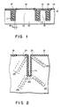
- a trench 11 is formed to surround an element region 12 of an Si substrate 13 by anisotropic etching.
- a nonoxide film 14 such as a silicon nitride (SiN x ) film is selectively formed on the upper surface of the element region 12.
- Thermal oxidation is performed for the resultant structure using the nonoxide film 14 as a mask to form an oxide film 15 on the inner surface of the trench 11 and the upper surface of a field region 16.
- a polysilicon layer 17 is buried in the trench 11, and after the surface of the polysilicon layer 17 is flattened, a capping oxide film 18 is formed on the trench 11.
- an interval W TL between the end of the nonoxide film 14 and the first side wall (indicated by broken line in Fig. 1) of the trench 11 is generally designed to be minimized.
- the interval W TL is conventionally selected from the range of 0 ⁇ m to 1 ⁇ m.
- dislocation defects 23 may be extended in the inside of the substrate from corner portions 21 of the upper portion of the trench 11 and corners 22 of the bottom by stress concentration upon formation of the oxide film 15 by thermal oxidation, as shown in Fig. 2.
- the dislocation defects cause degradation of isolation characteristics between element regions and characteristics of elements formed on the element regions.
- the presence of dislocation defects causes a leak current of each transistor to increase or causes various characteristics such as collector current (Ic) vs. current amplification factor (h FE ) characteristics to degrade.
- Ic collector current
- h FE current amplification factor
- dislocation defects are present at a given density, a recombination current is increased using defects as the center of recombination, thereby degrading characteristics of the element or element isolation characteristics.
- a method of manufacturing a semiconductor device comprising the steps of: forming a trench in a monocrystalline silicon substrate to surround an element forming region by anisotropic etching, forming a nonoxide film on the element forming region such that an interval between an end portion of the nonoxide film and a side wall of each trench at a side near the element forming region of the trench is not less than 2 ⁇ m, and forming an oxide film having a thickness of less than 9,000 ⁇ on a surface of the substrate including an inside of the trench using the nonoxide film as a mask during selective oxidation.
- an element isolation structure using a trench is formed by the following manner. After a trench is formed in a semiconductor substrate, oxide films are simultaneously or independently formed in the trench and on the upper surface of a field region by thermal oxidation using a nonoxide film such as an SiN x film as a mask, and a dielectric material such as polysilicon is filled in the trench upon oxidation. Thereafter, the surface of the polysilicon is flattened, and the exposed surface of the dielectric material is oxidized to form a capping oxide film.
- a density of defects such as dislocation extending from the corner of the trench mainly depends on an interval (interval W TL in Fig.
- a density of defects such as dislocation extending from the corners of the trench also depends on the thickness of an oxide film formed on a field region or the inner surface of the trench. According to an attempt to be described later, the thickness of the oxide film formed by oxidizing the field region and the inner surface of the trench and the interval between the end of the nonoxide film and the first side wall of the trench are defined, thereby surely suppressing dislocation defects extending from the corners of the trench. Therefore, element characteristics and element isolation characteristics are not substantially degraded.
- an SiO2 film 31 having a thickness of 700 to 1,000 ⁇ is formed on the major surface of a monocrystalline silicon substrate 32 by CVD or thermal oxidation.
- a resist pattern 33 having an opening on a region for forming a trench for isolating elements is formed in the SiO2 film 31, and a plurality of trenches 34 each having a width W T of about 1 to 2 ⁇ m and a depth of about 5 ⁇ m are formed vertically in the substrate to surround a plurality of element regions 35.
- the monocrystalline silicon substrate 32 is constituted by, e.g., a p-type epitaxial layer 36, an n+-type buried layer 37 formed on the epitaxial layer 36, and an n-type layer 38 formed on the n+-type buried layer 37.
- the resist pattern 33 is removed by, e.g., an O2 asher, and the SiO2 film 31 is removed by, e.g., diluted hydrofluoric acid.
- thermal oxidation is performed for the resultant structure in a gas mixture of H2 and O2 at a temperature of 950°C to form an SiO2 film 39 having a thickness of about 500 ⁇ on the entire surface of the resultant structure.
- a 1,500 ⁇ nonoxide film 40 such as a silicon nitride (SiN x ) film is deposited at a temperature of 780°C by LP-CVD (Low Pressure-CVD).
- a resist pattern 41 is formed on the nonoxide film 40 by photoetching, and the nonoxide film 40 is plasma-etched to leave it on only the plurality of element regions 35.
- the device is designed to have an interval (W TL in Fig. 3B) having at least 2 ⁇ m or more between the end of the remaining nonoxide film 40 and a side wall of each trench 34 at a side near the element region 35.
- the device is designed to have an interval (W TT in Fig. 3B) having about 3 ⁇ m between side walls of the adjacent trenches 34.
- the resist pattern 41 is removed by, e.g., an O2 asher in the same manner as described above, and wet oxidation is performed at a temperature of 1,000°C using the nonoxide film 40 as a mask to continuously form, e.g., oxide films 43 each having a thickness of less than 9,000 ⁇ , e.g., 8,000 ⁇ , on field regions 42 respectively located between the element regions 35 and the trenches 34 and on the side walls of trenches 34.
- oxide films 43 each having a thickness of less than 9,000 ⁇ , e.g., 8,000 ⁇
- a polysilicon layer 44 is buried by, e.g., LP-CVD in the trenches 34 in which the oxide films 43 are formed. After the surface of the polysilicon layer 44 is flattened, the exposed surface of the polysilicon layer 44 is oxidized to form a thin capping oxide film 45.
- a bipolar transistor is formed on each of the plurality of element regions 35 by the known method. Note that reference symbols E, B, and C denote emitter, base, and collector regions of the bipolar transistor, respectively.
- p+-type channel cut regions 46 are respectively formed in the bottoms of the trenches by ion implantation or diffusion.
- the interval W TL was set to be various values, and characteristics of an integrated circuit wherein a plurality of bipolar transistors were formed on the substrate by the above described method were estimated.
- the intervals W TL were 0 ⁇ m, 1 ⁇ m, 2 ⁇ m, 3 ⁇ m, and 4 ⁇ m
- the thickness of all the oxide films 43 on the field region 42 was 9,000 ⁇
- the interval (W TT in Fig. 3B) between the trenches was 3 ⁇ m.
- estimation items included densities of defects generated at corner portions of the top and bottom of each trench, a stress applied around each trench at room temperature, and a leak voltage generated between elements.
- the above defect density was represented as follows. After completion of all element forming steps, the entire surface of the substrate was etched to expose the trench, and defects present on the exposed surface of the trench were selectively etched by wright etching or the like. Thereafter, the number of defects was visually counted using an optical microscope, and the number was represented as a defect density per 1-mm trench length. The stress was measured by Micro-Raman-Spectroscopy, and a maximum stress applied to the bottom of the trench was represented as a measured value. In addition, a leak current was calculated from voltage vs. current characteristics between both the collector electrodes of two transistors, and the leak current was represented as a leak current density between elements at a voltage of 12 V.
- Fig. 4 The abscissa in Fig. 4 represents the interval W TL ( ⁇ m), and the ordinate represents the leak current density (A/cm2) between transistors at a voltage of 12 V, the defect density (defects/mm), and the stress (dyne/cm2).
- Fig. 5 shows a relationship between the interval W TL and a non-defective rate of transistors in a case wherein 200 to 500 npn transistors are formed on one silicon substrate.
- a non-defective element has a collector current I CEO of 1 ⁇ A or less when a voltage of 5 V is applied between the collector and emitter electrodes and the base electrode is open.
- I CEO collector current
- a non-defective rate is gradually decreased.
- the interval is 0 ⁇ m, the non-defective rate is rapidly decreased. Therefore, according to this characteristic, the minimum interval W TL is given as 1 ⁇ m.
- Fig. 6 shows collector current (Ic) vs. current amplification factor (hFE) characteristics of an npn transistor formed on a silicon substrate using the interval W TL as a parameter. That is, the abscissa represents the collector current Ic (A), and the ordinate represents the current amplification factor h FE . Note that the h FE falls within the range of 80 to 100. As is apparent from Fig. 6, when the interval W TL is smaller than 2 ⁇ m, h FE is decreased in a region having a low collector current.
- the minimum interval W TL is given as 2 ⁇ m. According to the above result, when bipolar transistors are formed on element regions, the interval W TL must be 2 ⁇ m or more in order to obtain the sufficiently satisfactory characteristics of the transistors.
- the thickness of the oxide film formed on the field region and the side walls of the trench by wet oxidation is generally designed to be less than 9,000 ⁇ .
- the oxide film extends outside the surface of the substrate by about 45% of its total thickness and extends inside the surface of the substrate by about 55% of its total thickness. Therefore, the trench is designed to have the width W T of 1 ⁇ m as described above, and an oxide film having a thickness of 8,000 ⁇ is formed by wet oxidation.
- an oxide film having a thickness of 8,000 ⁇ ⁇ 0.45, i.e., 3,600 ⁇ is formed on the first surface of the trench.
- the trench is not buried by only the oxide film. Therefore, a polysilicon layer can be formed in the trench.
- each of trenches 34 has a width W T of 1 to 2 ⁇ m and a depth L T of about 5 ⁇ m, an interval W TL between the end of a nonoxide film 40 and the side wall of the trench 34 is at least 2 ⁇ m or more, and an oxide film 43 has a thickness of less than 9,000 ⁇ , e.g., 8,000 ⁇ .
- shrinkage the integrated circuit is designed to have sizes obtained by multiplying a predetermined magnification, e.g., 0.8 or 0.7, by a standard size, and all the sizes are reduced proportionally to the magnification.
- each trench 34 has a width W T of 0.8 to 1.6 ⁇ m and a depth L T of about 4 ⁇ m, an interval W TL between the end of a nonoxide film 40 and the side wall of a trench 34 is at least 1.6 ⁇ m or more, and the thickness of an oxide film 43 is designed to have less than 7,200 ⁇ , e.g., 7,000 ⁇ .
- shrinkage is performed at a magnification of 0.7 for the integrated circuit designed and manufactured by the above embodiment in Fig.
- each trench 34 has a width W T of 0.7 to 1.4 ⁇ m and a depth L T of about 3.5 ⁇ m, an interval W TL between the end of a nonoxide film 40 and the side wall of a trench 34 is at least 1.4 ⁇ m or more, and the thickness of an oxide film 43 is designed to have less than 6,300 ⁇ , e.g., 6,000 ⁇ .
- the present invention is not limited to the above embodiments and can be variously changed.
- the oxide films may be independently formed inside the trench and on the upper surface of the field region.
Landscapes
- Element Separation (AREA)
- Local Oxidation Of Silicon (AREA)
Applications Claiming Priority (2)
| Application Number | Priority Date | Filing Date | Title |
|---|---|---|---|
| JP15154289 | 1989-06-14 | ||
| JP151542/89 | 1989-06-14 |
Publications (3)
| Publication Number | Publication Date |
|---|---|
| EP0402897A2 true EP0402897A2 (fr) | 1990-12-19 |
| EP0402897A3 EP0402897A3 (fr) | 1993-12-15 |
| EP0402897B1 EP0402897B1 (fr) | 1998-08-19 |
Family
ID=15520790
Family Applications (1)
| Application Number | Title | Priority Date | Filing Date |
|---|---|---|---|
| EP90111198A Expired - Lifetime EP0402897B1 (fr) | 1989-06-14 | 1990-06-13 | Procédé pour la fabrication de dispositifs semi-conducteurs comportant des composants isolés par des rainures |
Country Status (4)
| Country | Link |
|---|---|
| EP (1) | EP0402897B1 (fr) |
| JP (1) | JP2839651B2 (fr) |
| KR (1) | KR930006594B1 (fr) |
| DE (1) | DE69032571T2 (fr) |
Cited By (2)
| Publication number | Priority date | Publication date | Assignee | Title |
|---|---|---|---|---|
| EP0544547A3 (en) * | 1991-11-28 | 1994-08-17 | Nec Corp | Method of forming an isolation region comprising a trench isolation region and a selective oxidation film involved in a semiconductor device |
| EP0451454A3 (en) * | 1990-02-09 | 1994-08-24 | Toshiba Kk | Semiconductor device having element regions being electrically isolated from each other |
Families Citing this family (3)
| Publication number | Priority date | Publication date | Assignee | Title |
|---|---|---|---|---|
| JP4657614B2 (ja) * | 2004-03-09 | 2011-03-23 | Okiセミコンダクタ株式会社 | 半導体装置及び半導体装置の製造方法 |
| JP5292984B2 (ja) * | 2008-08-08 | 2013-09-18 | 株式会社デンソー | 半導体装置の製造方法 |
| JP5691074B2 (ja) | 2008-08-20 | 2015-04-01 | ルネサスエレクトロニクス株式会社 | 半導体装置の製造方法 |
Family Cites Families (3)
| Publication number | Priority date | Publication date | Assignee | Title |
|---|---|---|---|---|
| US4472873A (en) * | 1981-10-22 | 1984-09-25 | Fairchild Camera And Instrument Corporation | Method for forming submicron bipolar transistors without epitaxial growth and the resulting structure |
| US4486266A (en) * | 1983-08-12 | 1984-12-04 | Tektronix, Inc. | Integrated circuit method |
| US4876214A (en) * | 1988-06-02 | 1989-10-24 | Tektronix, Inc. | Method for fabricating an isolation region in a semiconductor substrate |
-
1990
- 1990-06-12 JP JP2153256A patent/JP2839651B2/ja not_active Expired - Lifetime
- 1990-06-13 EP EP90111198A patent/EP0402897B1/fr not_active Expired - Lifetime
- 1990-06-13 DE DE69032571T patent/DE69032571T2/de not_active Expired - Fee Related
- 1990-06-14 KR KR1019900008734A patent/KR930006594B1/ko not_active Expired - Fee Related
Cited By (3)
| Publication number | Priority date | Publication date | Assignee | Title |
|---|---|---|---|---|
| EP0451454A3 (en) * | 1990-02-09 | 1994-08-24 | Toshiba Kk | Semiconductor device having element regions being electrically isolated from each other |
| EP0544547A3 (en) * | 1991-11-28 | 1994-08-17 | Nec Corp | Method of forming an isolation region comprising a trench isolation region and a selective oxidation film involved in a semiconductor device |
| US5474953A (en) * | 1991-11-28 | 1995-12-12 | Nec Corporation | Method of forming an isolation region comprising a trench isolation region and a selective oxidation film involved in a semiconductor device |
Also Published As
| Publication number | Publication date |
|---|---|
| JPH03183152A (ja) | 1991-08-09 |
| KR930006594B1 (ko) | 1993-07-21 |
| JP2839651B2 (ja) | 1998-12-16 |
| EP0402897A3 (fr) | 1993-12-15 |
| DE69032571T2 (de) | 1999-02-04 |
| DE69032571D1 (de) | 1998-09-24 |
| KR910001938A (ko) | 1991-01-31 |
| EP0402897B1 (fr) | 1998-08-19 |
Similar Documents
| Publication | Publication Date | Title |
|---|---|---|
| US4693781A (en) | Trench formation process | |
| US5384280A (en) | Method of manufacturing a semiconductor device isolated by a trench | |
| EP0061855B1 (fr) | Procédé de fabrication d'un élément semiconducteur | |
| US4546538A (en) | Method of manufacturing semiconductor integrated circuit devices having dielectric isolation regions | |
| EP0395358B1 (fr) | Méthode de fabrication d'un transistor bipolaire | |
| EP0098374B1 (fr) | Structure d'isolation diélectrique pour circuits intégrés et procédé pour la fabrication de cette structure | |
| KR960006714B1 (ko) | 반도체 장치의 제조 방법 | |
| EP0073370B1 (fr) | Structure de circuit intégré et procédé pour la formation d'une structure à isolation encastrée pour circuits intégrés | |
| US4641416A (en) | Method of making an integrated circuit structure with self-aligned oxidation to isolate extrinsic base from emitter | |
| US4725874A (en) | Semiconductor device having protected edges | |
| US6750526B2 (en) | Semiconductor device with trench isolation having reduced leak current | |
| US4824797A (en) | Self-aligned channel stop | |
| US4661832A (en) | Total dielectric isolation for integrated circuits | |
| EP0091984A2 (fr) | Dispositifs à circuits intégrés comprenant des régions d'isolation diélectriques et procédé pour la fabrication de ces dispositifs | |
| US5834360A (en) | Method of forming an improved planar isolation structure in an integrated circuit | |
| US4992843A (en) | Collector contact of an integrated bipolar transistor | |
| US20030170964A1 (en) | Oxidation of ion implanted semiconductors | |
| US5332683A (en) | Method of manufacturing semiconductor device having elements isolated by trench | |
| US4047195A (en) | Semiconductor structure | |
| EP0068275A2 (fr) | Procédé pour la fabrication de dispositifs semiconducteur utilisant l'attaque de matériaux par ions réactifs | |
| EP0520703A1 (fr) | Procédé pour la fabrication de régions d'oxyde de champ | |
| EP0435550B1 (fr) | Dispositif à semiconducteur ayant une région d'isolation diélectrique d'une structure de rainure en forme de U | |
| EP0402897B1 (fr) | Procédé pour la fabrication de dispositifs semi-conducteurs comportant des composants isolés par des rainures | |
| EP0451454B1 (fr) | Procédé de fabrication d'un dispositif semi-conducteur comportant des composants électriquement isolés entre eux | |
| US4746623A (en) | Method of making bipolar semiconductor device with wall spacer |
Legal Events
| Date | Code | Title | Description |
|---|---|---|---|
| PUAI | Public reference made under article 153(3) epc to a published international application that has entered the european phase |
Free format text: ORIGINAL CODE: 0009012 |
|
| 17P | Request for examination filed |
Effective date: 19900613 |
|
| AK | Designated contracting states |
Kind code of ref document: A2 Designated state(s): DE FR GB |
|
| PUAL | Search report despatched |
Free format text: ORIGINAL CODE: 0009013 |
|
| AK | Designated contracting states |
Kind code of ref document: A3 Designated state(s): DE FR GB |
|
| 17Q | First examination report despatched |
Effective date: 19940131 |
|
| GRAG | Despatch of communication of intention to grant |
Free format text: ORIGINAL CODE: EPIDOS AGRA |
|
| GRAG | Despatch of communication of intention to grant |
Free format text: ORIGINAL CODE: EPIDOS AGRA |
|
| GRAH | Despatch of communication of intention to grant a patent |
Free format text: ORIGINAL CODE: EPIDOS IGRA |
|
| GRAH | Despatch of communication of intention to grant a patent |
Free format text: ORIGINAL CODE: EPIDOS IGRA |
|
| GRAA | (expected) grant |
Free format text: ORIGINAL CODE: 0009210 |
|
| AK | Designated contracting states |
Kind code of ref document: B1 Designated state(s): DE FR GB |
|
| REF | Corresponds to: |
Ref document number: 69032571 Country of ref document: DE Date of ref document: 19980924 |
|
| ET | Fr: translation filed | ||
| PLBE | No opposition filed within time limit |
Free format text: ORIGINAL CODE: 0009261 |
|
| STAA | Information on the status of an ep patent application or granted ep patent |
Free format text: STATUS: NO OPPOSITION FILED WITHIN TIME LIMIT |
|
| 26N | No opposition filed | ||
| REG | Reference to a national code |
Ref country code: GB Ref legal event code: IF02 |
|
| PGFP | Annual fee paid to national office [announced via postgrant information from national office to epo] |
Ref country code: DE Payment date: 20070607 Year of fee payment: 18 |
|
| PGFP | Annual fee paid to national office [announced via postgrant information from national office to epo] |
Ref country code: GB Payment date: 20070613 Year of fee payment: 18 |
|
| PGFP | Annual fee paid to national office [announced via postgrant information from national office to epo] |
Ref country code: FR Payment date: 20070608 Year of fee payment: 18 |
|
| GBPC | Gb: european patent ceased through non-payment of renewal fee |
Effective date: 20080613 |
|
| REG | Reference to a national code |
Ref country code: FR Ref legal event code: ST Effective date: 20090228 |
|
| PG25 | Lapsed in a contracting state [announced via postgrant information from national office to epo] |
Ref country code: DE Free format text: LAPSE BECAUSE OF NON-PAYMENT OF DUE FEES Effective date: 20090101 |
|
| PG25 | Lapsed in a contracting state [announced via postgrant information from national office to epo] |
Ref country code: GB Free format text: LAPSE BECAUSE OF NON-PAYMENT OF DUE FEES Effective date: 20080613 |
|
| PG25 | Lapsed in a contracting state [announced via postgrant information from national office to epo] |
Ref country code: FR Free format text: LAPSE BECAUSE OF NON-PAYMENT OF DUE FEES Effective date: 20080630 |