EP0403287B1 - Verfahren zum Polieren von Halbleiterplättchen - Google Patents
Verfahren zum Polieren von Halbleiterplättchen Download PDFInfo
- Publication number
- EP0403287B1 EP0403287B1 EP90306519A EP90306519A EP0403287B1 EP 0403287 B1 EP0403287 B1 EP 0403287B1 EP 90306519 A EP90306519 A EP 90306519A EP 90306519 A EP90306519 A EP 90306519A EP 0403287 B1 EP0403287 B1 EP 0403287B1
- Authority
- EP
- European Patent Office
- Prior art keywords
- semiconductor wafer
- polishing
- thickness
- wafer
- polished
- Prior art date
- Legal status (The legal status is an assumption and is not a legal conclusion. Google has not performed a legal analysis and makes no representation as to the accuracy of the status listed.)
- Expired - Lifetime
Links
- 239000004065 semiconductor Substances 0.000 title claims description 96
- 238000007517 polishing process Methods 0.000 title claims description 5
- 238000005498 polishing Methods 0.000 claims description 54
- 229910052710 silicon Inorganic materials 0.000 claims description 9
- 239000010703 silicon Substances 0.000 claims description 9
- VYPSYNLAJGMNEJ-UHFFFAOYSA-N Silicium dioxide Chemical compound O=[Si]=O VYPSYNLAJGMNEJ-UHFFFAOYSA-N 0.000 claims description 7
- 239000011159 matrix material Substances 0.000 claims description 7
- 229910052814 silicon oxide Inorganic materials 0.000 claims description 5
- 229910052581 Si3N4 Inorganic materials 0.000 claims description 3
- 238000003825 pressing Methods 0.000 claims description 3
- HQVNEWCFYHHQES-UHFFFAOYSA-N silicon nitride Chemical compound N12[Si]34N5[Si]62N3[Si]51N64 HQVNEWCFYHHQES-UHFFFAOYSA-N 0.000 claims description 3
- 235000012431 wafers Nutrition 0.000 description 116
- 239000011521 glass Substances 0.000 description 21
- 230000001105 regulatory effect Effects 0.000 description 14
- 238000000034 method Methods 0.000 description 12
- 239000004744 fabric Substances 0.000 description 9
- 239000002344 surface layer Substances 0.000 description 9
- XUIMIQQOPSSXEZ-UHFFFAOYSA-N Silicon Chemical compound [Si] XUIMIQQOPSSXEZ-UHFFFAOYSA-N 0.000 description 8
- 239000000463 material Substances 0.000 description 6
- 238000002474 experimental method Methods 0.000 description 4
- HEMHJVSKTPXQMS-UHFFFAOYSA-M Sodium hydroxide Chemical compound [OH-].[Na+] HEMHJVSKTPXQMS-UHFFFAOYSA-M 0.000 description 3
- 239000007864 aqueous solution Substances 0.000 description 2
- 238000005229 chemical vapour deposition Methods 0.000 description 2
- 239000008119 colloidal silica Substances 0.000 description 2
- 238000007796 conventional method Methods 0.000 description 2
- 230000000694 effects Effects 0.000 description 2
- 238000005530 etching Methods 0.000 description 2
- 239000002184 metal Substances 0.000 description 2
- 239000002002 slurry Substances 0.000 description 2
- VHUUQVKOLVNVRT-UHFFFAOYSA-N Ammonium hydroxide Chemical compound [NH4+].[OH-] VHUUQVKOLVNVRT-UHFFFAOYSA-N 0.000 description 1
- 229930091051 Arenine Natural products 0.000 description 1
- 239000006061 abrasive grain Substances 0.000 description 1
- 235000011114 ammonium hydroxide Nutrition 0.000 description 1
- 238000006243 chemical reaction Methods 0.000 description 1
- 239000003795 chemical substances by application Substances 0.000 description 1
- 238000011109 contamination Methods 0.000 description 1
- 239000003822 epoxy resin Substances 0.000 description 1
- 239000010419 fine particle Substances 0.000 description 1
- 239000012212 insulator Substances 0.000 description 1
- 238000004519 manufacturing process Methods 0.000 description 1
- 238000012986 modification Methods 0.000 description 1
- 230000004048 modification Effects 0.000 description 1
- 230000003647 oxidation Effects 0.000 description 1
- 238000007254 oxidation reaction Methods 0.000 description 1
- 229920000647 polyepoxide Polymers 0.000 description 1
Images


Classifications
-
- B—PERFORMING OPERATIONS; TRANSPORTING
- B24—GRINDING; POLISHING
- B24B—MACHINES, DEVICES, OR PROCESSES FOR GRINDING OR POLISHING; DRESSING OR CONDITIONING OF ABRADING SURFACES; FEEDING OF GRINDING, POLISHING, OR LAPPING AGENTS
- B24B37/00—Lapping machines or devices; Accessories
- B24B37/005—Control means for lapping machines or devices
- B24B37/013—Devices or means for detecting lapping completion
Definitions
- the present invention relates to a method of polishing semiconductor wafers, more particularly to an effective technique suitable for polishing semiconductor wafers, whose surfaces to be polished are required to be very flat.
- the final step of manufacturing semiconductor silicon wafers includes a polishing step for forming a specular surface.
- This step generally employs a method called the mechanochemical method, which combines mechanical attrition and chemical reaction.
- Fig. 4 shows the main components of a polishing apparatus for polishing one face of a semiconductor wafer.
- numeral 1 indicates a glass plate.
- a plurality of semiconductor wafers 2 are bonded with wax to the under surface of the glass plate 1.
- These semiconductor wafers 2, having undergone processes such as lapping, beveling and etching, are bonded in such a manner that they can be attached or removed.
- a polishing cloth 3a is firmly held on the surface of a turntable 3, which is positioned under the glass plate 1. Polishing is performed by using the apparatus in the following way.
- the semiconductor wafer 2 contacts the polishing cloth 3a under the pressure of the glass plate 1.
- the turntable 3 rotates to cause the glass plate 1, supporting the semiconductor wafer 2, to rotate so as to bring the semiconductor wafer 2 into contact with the polishing cloth 3a on which polishing slurry is sprayed.
- the polishing slurry is a weak alkaline aqueous solution containing colloidal silica as fine abrasive grains.
- US-A-2 979 868 describes a lapping machine for polishing a semiconductor wafer which includes thickness-regulating members.
- the thickness-regulating members preferably consist of a hard metal.
- contamination may be a problem when using a metal.
- the present invention discloses a method of polishing a semiconductor wafer according to the single claim.
- the semiconductor wafer bonded to a plate is polished to a desired thickness by pressing the semiconductor wafer against a rotating turntable side.
- the semiconductor wafer is bonded to the plate, and at the same time, thickness regulating members whose surface layer is made of a material where polishing speed is slower than the semiconductor wafer, are arranged on the plane of the plate in order to control the thickness of the semiconductor wafer.
- a semiconductor wafer to be polished is bonded to a plate, and at the same time, the thickness regulating members, whose surface layer is made of a material where polishing speed is slower than the semiconductor wafer, are arranged around the bonded semiconductor wafer and closely spaced-apart from it on the plane of the plate.
- the semiconductor wafer is polished by using the thickness regulating member as a stopper. For these reasons, even if the polishing speed increases under circumstances that the semiconductor wafer is pressed to the turntable at increased pressure, a part of the pressure is to be borne by the thickness regulating member when the polishing is just about finished.
- the polishing speed becomes slow according to the increase in the pressure applied to the wafer by the amount of the pressure borne as mentioned above, and thus it is easy to control the polishing amount of the semiconductor wafer as well as the thickness of the semiconductor wafer.
- the polished surface of the semiconductor wafer thus becomes even in thickness variation across and specular.
- the thickness regulating member arranged around the semiconductor wafer, acts as a stopper, the semiconductor wafer is so polished that the surface of the thickness regulating member on the turntable side is substantially flush with the semiconductor wafer, thereby contributing to a less uneven thickness across the whole surface of the semiconductor wafer where one surface is the surface to be polished.
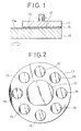
- Fig. 1 shows the major components of a polishing apparatus for polishing one face of the semiconductor wafer.
- one semiconductor wafer 12 having undergone processes such as lapping, beveling and etching is bonded with wax to the central under surface of the glass plate 11.
- a total of eight dummy wafers 15, serving as thickness regulating members are so arranged on the under surface of the glass plate 11 as to encircle the above semiconductor wafer 12.
- the semiconductor wafer 12 is bonded to the surface of the glass plate 11 after molten wax is uniformly sprayed in very fine particles by a sprayer on the surface of the wafer 12 to be bonded; or the semiconductor wafer 12 and the dummy wafers 15 are heated after being just placed on the surface of the glass plate 11, and then the wax is introduced to the gaps under the wafers having been melted at a point of the periphery already warmed up before the semiconductor wafer 12 and the dummy wafers 15 are pressed and cooled to fix in order to decrease the gaps and thus clear the severest precision of less than 0 ⁇ .1 ⁇ m.
- the surface layers of the dummy wafers 15 are made of a material slower to polish than the semiconductor wafer 12.
- the matrix of the dummy wafer 15 is made of silicon and a silicon oxide or silicon nitride film is formed on the surface layer of the dummy wafer 15.
- the silicon oxide film may be a thermal oxide film or an oxide film obtained by chemical vapor deposition method (CVD) and is preferably a thermal oxide film, which is slower to remove in polishing by the mechanochemical polishing method.
- the dummy wafers 15 are bonded with wax to the glass plate 11 in the same manner as in the semiconductor wafer 12, that is, they can be attached or removed, or they are bonded semipermanently with epoxy resin or the like to the glass plate 11.
- the dummy wafer 15 is made of a material considerably slower to polish than the semiconductor wafer 12, it is convenient to bond the dummy wafer 15 semipermanently to the glass plate 11.
- the matrix of the dummy wafer 15 is made of silicon, it is possible to control the thickness of the semiconductor 12 very effectively and accurately.
- a polishing cloth 13a is bonded to the upper surface of the turntable 11 under the glass plate 11.
- Polishing is performed by using the polishing apparatus as follows: the semiconductor wafer 12 contacts the polishing cloth 13a under the pressure of the glass plate 11. At the same time, the turntable 13 rotates to cause the glass plate 11, supporting the semiconductor wafer 12, to rotate so as to bring the semiconductor wafer 12 into contact with the polishing cloth 13a. As a result, the main surface of the semiconductor wafer 12 bonded to the under surface of the glass plate 11 is polished.
- a polishing agent during the polishing operation, colloidal silica, dispersed in an aqueous solution with a pH adjusted to weak alkalinity with NaOH or NH4OH, is employed.
- the semiconductor wafer 12 to be polished is bonded to the central under surface of the glass plate 11, and at the same time, dummy wafers 15, made of a material slower to polish than the semiconductor wafer 12, are arranged around the semiconductor 12 under the glass plate 11.
- the polishing speed for the dummy wafer 15 is, depending upon polishing conditions, 1/20 ⁇ 0 ⁇ or less of the polishing speed of the silicon.
- the semiconductor wafer 12 is polished by using the dummy wafers 15 as a stopper, even if polishing speed increases owing to the condition that the semiconductor wafer 12 is pressed to the turntable 11 under increased pressure, part of the pressure will be borne by the dummy wafers 15 through the whole polishing operation. As a result, the polishing speed slows according to an amount of the pressure shared with the dummy wafers, and thus it is easy to control the polishing amount of the semiconductor wafer 12 as well as the thickness across the whole surface of the semiconductor wafer 12. The polished surface of the semiconductor wafer 12 thus becomes even in thickness across and specular.
- the semiconductor wafer 12 is so polished that the surfaces of the dummy wafers 15 on the turntable side 11 are substantially flush with the semiconductor wafer 12, thereby contributing to a less uneven thickness of the semiconductor wafer 12 where one surface is the surface to be polished. For all the reasons described above, a highly geometrically controlled semiconductor wafer 12 can be obtained.
- Fig. 3 there are nine positions for measuring the thickness of the semiconductor wafer.
- the dummy wafer 15 whose matrix is silicon and with a silicon oxide film formed on its surface layer
- a dummy wafer whose matrix is silicon and with a silicon nitride film formed on its surface layer
- the shape of the dummy wafer is not necessarily the same as that of the semiconductor wafer.
- a ring-shaped dummy wafer can be employed so as to encircle the semiconductor wafer 12.
- the important thing to be considered is to use a dummy wafer, which is capable of sharing part of the pressure used to polish the semiconductor wafer on the turntable and which is capable of serving as a stopper.
- the semiconductor wafer is polished to its desired thickness by pressing it against the rotating turntable side, the semiconductor wafer is bonded to the plate, and at the same time, the thickness regulating member, whose surface layer is made of a material slower to polish than the semiconductor wafer, is arranged on the plane of the plate.
- the thickness regulating member controls the semiconductor wafer thickness. For these reasons, even if the polishing speed increases, it becomes easy to control the polishing amount of the semiconductor wafer.
- the semiconductor wafer is not polished to a thinner thickness than the thickness of the thickness regulating member. As a result, the uneven thickness of a semiconductor wafer where one surface is the surface to be polished is reduced and thus a highly geometrically controlled semiconductor wafer can be obtained.
Landscapes
- Engineering & Computer Science (AREA)
- Mechanical Engineering (AREA)
- Mechanical Treatment Of Semiconductor (AREA)
- Finish Polishing, Edge Sharpening, And Grinding By Specific Grinding Devices (AREA)
Claims (1)
- Verfahren zum Polieren oder Schleifen einer Halbleiterscheibe (12) auf eine gewünschte Dicke durch Andrücken der Halbleiterscheibe gegen einen Tisch (13) unter Relativdrehung, und bei dem die gewünschte Dicke durch die Bereitstellung einer Mehrzahl von dickeregulierenden Elementen (15) bestimmt wird, deren Oberflächen beständiger als die Halbleiterscheibe gegen Polieren/Schleifen sind, dadurch gekennzeichnet, daß die Scheibe mit der Mitte einer Platte (11) verbunden wird, die Elemente (15) in einer Matrix um die Scheibe herum angeordnet werden und jedes Element aus Silizium mit einem Siliziumoxid- oder Siliziumnitridfilm an seiner Oberfläche hergestellt ist.
Applications Claiming Priority (2)
| Application Number | Priority Date | Filing Date | Title |
|---|---|---|---|
| JP1153748A JPH0319336A (ja) | 1989-06-16 | 1989-06-16 | 半導体ウェーハの研磨方法 |
| JP153748/89 | 1989-06-16 |
Publications (3)
| Publication Number | Publication Date |
|---|---|
| EP0403287A2 EP0403287A2 (de) | 1990-12-19 |
| EP0403287A3 EP0403287A3 (de) | 1991-10-23 |
| EP0403287B1 true EP0403287B1 (de) | 1994-10-05 |
Family
ID=15569254
Family Applications (1)
| Application Number | Title | Priority Date | Filing Date |
|---|---|---|---|
| EP90306519A Expired - Lifetime EP0403287B1 (de) | 1989-06-16 | 1990-06-14 | Verfahren zum Polieren von Halbleiterplättchen |
Country Status (3)
| Country | Link |
|---|---|
| EP (1) | EP0403287B1 (de) |
| JP (1) | JPH0319336A (de) |
| DE (1) | DE69013065T2 (de) |
Cited By (1)
| Publication number | Priority date | Publication date | Assignee | Title |
|---|---|---|---|---|
| CN105199610A (zh) * | 2015-10-16 | 2015-12-30 | 郑州磨料磨具磨削研究所有限公司 | 一种蓝宝石抛光组合物及其制备方法 |
Families Citing this family (5)
| Publication number | Priority date | Publication date | Assignee | Title |
|---|---|---|---|---|
| US5366924A (en) * | 1992-03-16 | 1994-11-22 | At&T Bell Laboratories | Method of manufacturing an integrated circuit including planarizing a wafer |
| US5445996A (en) * | 1992-05-26 | 1995-08-29 | Kabushiki Kaisha Toshiba | Method for planarizing a semiconductor device having a amorphous layer |
| GB2275129B (en) * | 1992-05-26 | 1997-01-08 | Toshiba Kk | Method for planarizing a layer on a semiconductor wafer |
| JP2778659B2 (ja) | 1993-12-24 | 1998-07-23 | キヤノン株式会社 | 導光体及び照明装置及び画像読取装置 |
| JP3983887B2 (ja) * | 1998-04-09 | 2007-09-26 | 沖電気工業株式会社 | 基板研磨用治具及び半導体ウエハの研磨方法 |
Citations (2)
| Publication number | Priority date | Publication date | Assignee | Title |
|---|---|---|---|---|
| JPS6471663A (en) * | 1987-09-08 | 1989-03-16 | Hitachi Cable | Lapping method for gaas wafer |
| JPH1051268A (ja) * | 1996-08-05 | 1998-02-20 | Toshiba Corp | 雑音消去に用いられるフィルタ演算装置及びフィルタ演算方法 |
Family Cites Families (5)
| Publication number | Priority date | Publication date | Assignee | Title |
|---|---|---|---|---|
| DE1110544B (de) * | 1957-11-29 | 1961-07-06 | Siemens Ag | Einscheiben-Laeppmaschine fuer Halbleiterscheiben |
| US3559346A (en) * | 1969-02-04 | 1971-02-02 | Bell Telephone Labor Inc | Wafer polishing apparatus and method |
| US4165584A (en) * | 1977-01-27 | 1979-08-28 | International Telephone And Telegraph Corporation | Apparatus for lapping or polishing materials |
| FR2521895A1 (fr) * | 1982-02-23 | 1983-08-26 | Ansermoz Raymond | Tasseau multiple pour le rodage, au lapidaire, de pieces en forme de lames minces |
| JPS6451268A (en) * | 1987-08-19 | 1989-02-27 | Sanyo Electric Co | Mechanical polishing method |
-
1989
- 1989-06-16 JP JP1153748A patent/JPH0319336A/ja active Pending
-
1990
- 1990-06-14 EP EP90306519A patent/EP0403287B1/de not_active Expired - Lifetime
- 1990-06-14 DE DE69013065T patent/DE69013065T2/de not_active Expired - Fee Related
Patent Citations (2)
| Publication number | Priority date | Publication date | Assignee | Title |
|---|---|---|---|---|
| JPS6471663A (en) * | 1987-09-08 | 1989-03-16 | Hitachi Cable | Lapping method for gaas wafer |
| JPH1051268A (ja) * | 1996-08-05 | 1998-02-20 | Toshiba Corp | 雑音消去に用いられるフィルタ演算装置及びフィルタ演算方法 |
Non-Patent Citations (1)
| Title |
|---|
| PATENT ABSTRACTS OF JAPAN vol. 13, no. 244 (M-834)(3592) 07 June 1989 ; & JP-A-1 051 268; & JP-A-64 051 268 * |
Cited By (2)
| Publication number | Priority date | Publication date | Assignee | Title |
|---|---|---|---|---|
| CN105199610A (zh) * | 2015-10-16 | 2015-12-30 | 郑州磨料磨具磨削研究所有限公司 | 一种蓝宝石抛光组合物及其制备方法 |
| CN105199610B (zh) * | 2015-10-16 | 2017-12-19 | 郑州磨料磨具磨削研究所有限公司 | 一种蓝宝石抛光组合物及其制备方法 |
Also Published As
| Publication number | Publication date |
|---|---|
| EP0403287A2 (de) | 1990-12-19 |
| EP0403287A3 (de) | 1991-10-23 |
| DE69013065D1 (de) | 1994-11-10 |
| DE69013065T2 (de) | 1995-01-26 |
| JPH0319336A (ja) | 1991-01-28 |
Similar Documents
| Publication | Publication Date | Title |
|---|---|---|
| US5191738A (en) | Method of polishing semiconductor wafer | |
| US5032544A (en) | Process for producing semiconductor device substrate using polishing guard | |
| JP3925580B2 (ja) | ウェーハ加工装置および加工方法 | |
| US6180020B1 (en) | Polishing method and apparatus | |
| US5702290A (en) | Block for polishing a wafer during manufacture of integrated circuits | |
| US4256535A (en) | Method of polishing a semiconductor wafer | |
| EP0737546B1 (de) | Haltevorrichtung für ein Substrat und Verfahren und Vorrichtung zum Polieren eines Substrates | |
| US3857123A (en) | Apparatus for waxless polishing of thin wafers | |
| EP0264572B1 (de) | Poliermaschine | |
| KR20010092732A (ko) | 배면 손상을 형성하는 반도체 웨이퍼 처리방법 | |
| US5643405A (en) | Method for polishing a semiconductor substrate | |
| US6271140B1 (en) | Coaxial dressing for chemical mechanical polishing | |
| US6406357B1 (en) | Grinding method, semiconductor device and method of manufacturing semiconductor device | |
| EP0860238B1 (de) | Poliervorrichtung | |
| EP0403287B1 (de) | Verfahren zum Polieren von Halbleiterplättchen | |
| US6004860A (en) | SOI substrate and a method for fabricating the same | |
| US6478977B1 (en) | Polishing method and apparatus | |
| US5934981A (en) | Method for polishing thin plate and apparatus for polishing | |
| JPS6365473B2 (de) | ||
| US20020049029A1 (en) | System and method for chemical mechanical polishing | |
| JPH01321161A (ja) | 研磨方法 | |
| US6254465B1 (en) | Method of machining wafer for making filmed head sliders and device for machining the same | |
| JPH11216661A (ja) | ウェーハの枚葉式研磨方法とその装置 | |
| JPS6319309B2 (de) | ||
| JPH06132264A (ja) | 研磨による半導体基板の作成方法 |
Legal Events
| Date | Code | Title | Description |
|---|---|---|---|
| PUAI | Public reference made under article 153(3) epc to a published international application that has entered the european phase |
Free format text: ORIGINAL CODE: 0009012 |
|
| AK | Designated contracting states |
Kind code of ref document: A2 Designated state(s): DE FR GB |
|
| PUAL | Search report despatched |
Free format text: ORIGINAL CODE: 0009013 |
|
| AK | Designated contracting states |
Kind code of ref document: A3 Designated state(s): DE FR GB |
|
| 17P | Request for examination filed |
Effective date: 19920416 |
|
| 17Q | First examination report despatched |
Effective date: 19930712 |
|
| GRAA | (expected) grant |
Free format text: ORIGINAL CODE: 0009210 |
|
| AK | Designated contracting states |
Kind code of ref document: B1 Designated state(s): DE FR GB |
|
| REF | Corresponds to: |
Ref document number: 69013065 Country of ref document: DE Date of ref document: 19941110 |
|
| ET | Fr: translation filed | ||
| PLBE | No opposition filed within time limit |
Free format text: ORIGINAL CODE: 0009261 |
|
| STAA | Information on the status of an ep patent application or granted ep patent |
Free format text: STATUS: NO OPPOSITION FILED WITHIN TIME LIMIT |
|
| 26N | No opposition filed | ||
| PGFP | Annual fee paid to national office [announced via postgrant information from national office to epo] |
Ref country code: GB Payment date: 19990609 Year of fee payment: 10 |
|
| PGFP | Annual fee paid to national office [announced via postgrant information from national office to epo] |
Ref country code: FR Payment date: 19990610 Year of fee payment: 10 |
|
| PGFP | Annual fee paid to national office [announced via postgrant information from national office to epo] |
Ref country code: DE Payment date: 19990614 Year of fee payment: 10 |
|
| PG25 | Lapsed in a contracting state [announced via postgrant information from national office to epo] |
Ref country code: GB Free format text: LAPSE BECAUSE OF NON-PAYMENT OF DUE FEES Effective date: 20000614 |
|
| GBPC | Gb: european patent ceased through non-payment of renewal fee |
Effective date: 20000614 |
|
| PG25 | Lapsed in a contracting state [announced via postgrant information from national office to epo] |
Ref country code: FR Free format text: LAPSE BECAUSE OF NON-PAYMENT OF DUE FEES Effective date: 20010228 |
|
| REG | Reference to a national code |
Ref country code: FR Ref legal event code: ST |
|
| PG25 | Lapsed in a contracting state [announced via postgrant information from national office to epo] |
Ref country code: DE Free format text: LAPSE BECAUSE OF NON-PAYMENT OF DUE FEES Effective date: 20010403 |