EP0403880A2 - Strahlungsabschirmung für thermoelektrisch gekühlte Infrarotdetektoren - Google Patents
Strahlungsabschirmung für thermoelektrisch gekühlte Infrarotdetektoren Download PDFInfo
- Publication number
- EP0403880A2 EP0403880A2 EP90110714A EP90110714A EP0403880A2 EP 0403880 A2 EP0403880 A2 EP 0403880A2 EP 90110714 A EP90110714 A EP 90110714A EP 90110714 A EP90110714 A EP 90110714A EP 0403880 A2 EP0403880 A2 EP 0403880A2
- Authority
- EP
- European Patent Office
- Prior art keywords
- radiation
- reflector
- detector
- set forth
- stage
- Prior art date
- Legal status (The legal status is an assumption and is not a legal conclusion. Google has not performed a legal analysis and makes no representation as to the accuracy of the status listed.)
- Granted
Links
- 230000005855 radiation Effects 0.000 title claims abstract description 119
- 238000001816 cooling Methods 0.000 claims description 17
- 238000000034 method Methods 0.000 claims description 13
- 230000003247 decreasing effect Effects 0.000 claims description 4
- 239000006096 absorbing agent Substances 0.000 claims description 3
- 230000002401 inhibitory effect Effects 0.000 claims 1
- 238000003384 imaging method Methods 0.000 abstract description 9
- 230000004907 flux Effects 0.000 description 12
- 230000008901 benefit Effects 0.000 description 7
- 230000006872 improvement Effects 0.000 description 7
- 230000003287 optical effect Effects 0.000 description 6
- 230000000694 effects Effects 0.000 description 5
- 238000007747 plating Methods 0.000 description 5
- 238000010521 absorption reaction Methods 0.000 description 4
- PCHJSUWPFVWCPO-UHFFFAOYSA-N gold Chemical compound [Au] PCHJSUWPFVWCPO-UHFFFAOYSA-N 0.000 description 4
- 239000010931 gold Substances 0.000 description 4
- 229910052737 gold Inorganic materials 0.000 description 4
- 230000003595 spectral effect Effects 0.000 description 4
- 238000004458 analytical method Methods 0.000 description 3
- 239000000463 material Substances 0.000 description 3
- 239000007787 solid Substances 0.000 description 3
- 229910000661 Mercury cadmium telluride Inorganic materials 0.000 description 2
- 239000004642 Polyimide Substances 0.000 description 2
- 238000004364 calculation method Methods 0.000 description 2
- 238000010276 construction Methods 0.000 description 2
- 238000010168 coupling process Methods 0.000 description 2
- 238000005859 coupling reaction Methods 0.000 description 2
- 229920001721 polyimide Polymers 0.000 description 2
- 230000009467 reduction Effects 0.000 description 2
- 239000011358 absorbing material Substances 0.000 description 1
- 239000000853 adhesive Substances 0.000 description 1
- 230000001070 adhesive effect Effects 0.000 description 1
- MCMSPRNYOJJPIZ-UHFFFAOYSA-N cadmium;mercury;tellurium Chemical compound [Cd]=[Te]=[Hg] MCMSPRNYOJJPIZ-UHFFFAOYSA-N 0.000 description 1
- 239000000919 ceramic Substances 0.000 description 1
- 238000000576 coating method Methods 0.000 description 1
- 230000001427 coherent effect Effects 0.000 description 1
- 238000010835 comparative analysis Methods 0.000 description 1
- 230000001186 cumulative effect Effects 0.000 description 1
- 230000000593 degrading effect Effects 0.000 description 1
- 230000001788 irregular Effects 0.000 description 1
- 238000012986 modification Methods 0.000 description 1
- 230000004048 modification Effects 0.000 description 1
- 238000005457 optimization Methods 0.000 description 1
- 238000013433 optimization analysis Methods 0.000 description 1
- 239000004033 plastic Substances 0.000 description 1
- 239000002985 plastic film Substances 0.000 description 1
- 229920006255 plastic film Polymers 0.000 description 1
- 238000005498 polishing Methods 0.000 description 1
- 210000001747 pupil Anatomy 0.000 description 1
- 239000000758 substrate Substances 0.000 description 1
- 238000001931 thermography Methods 0.000 description 1
Images

Classifications
-
- H—ELECTRICITY
- H10—SEMICONDUCTOR DEVICES; ELECTRIC SOLID-STATE DEVICES NOT OTHERWISE PROVIDED FOR
- H10F—INORGANIC SEMICONDUCTOR DEVICES SENSITIVE TO INFRARED RADIATION, LIGHT, ELECTROMAGNETIC RADIATION OF SHORTER WAVELENGTH OR CORPUSCULAR RADIATION
- H10F77/00—Constructional details of devices covered by this subclass
- H10F77/60—Arrangements for cooling, heating, ventilating or compensating for temperature fluctuations
-
- F—MECHANICAL ENGINEERING; LIGHTING; HEATING; WEAPONS; BLASTING
- F25—REFRIGERATION OR COOLING; COMBINED HEATING AND REFRIGERATION SYSTEMS; HEAT PUMP SYSTEMS; MANUFACTURE OR STORAGE OF ICE; LIQUEFACTION SOLIDIFICATION OF GASES
- F25B—REFRIGERATION MACHINES, PLANTS OR SYSTEMS; COMBINED HEATING AND REFRIGERATION SYSTEMS; HEAT PUMP SYSTEMS
- F25B21/00—Machines, plants or systems, using electric or magnetic effects
- F25B21/02—Machines, plants or systems, using electric or magnetic effects using Peltier effect; using Nernst-Ettinghausen effect
-
- G—PHYSICS
- G01—MEASURING; TESTING
- G01J—MEASUREMENT OF INTENSITY, VELOCITY, SPECTRAL CONTENT, POLARISATION, PHASE OR PULSE CHARACTERISTICS OF INFRARED, VISIBLE OR ULTRAVIOLET LIGHT; COLORIMETRY; RADIATION PYROMETRY
- G01J5/00—Radiation pyrometry, e.g. infrared or optical thermometry
- G01J5/02—Constructional details
- G01J5/06—Arrangements for eliminating effects of disturbing radiation; Arrangements for compensating changes in sensitivity
-
- H—ELECTRICITY
- H10—SEMICONDUCTOR DEVICES; ELECTRIC SOLID-STATE DEVICES NOT OTHERWISE PROVIDED FOR
- H10F—INORGANIC SEMICONDUCTOR DEVICES SENSITIVE TO INFRARED RADIATION, LIGHT, ELECTROMAGNETIC RADIATION OF SHORTER WAVELENGTH OR CORPUSCULAR RADIATION
- H10F77/00—Constructional details of devices covered by this subclass
- H10F77/30—Coatings
- H10F77/306—Coatings for devices having potential barriers
- H10F77/331—Coatings for devices having potential barriers for filtering or shielding light, e.g. multicolour filters for photodetectors
- H10F77/334—Coatings for devices having potential barriers for filtering or shielding light, e.g. multicolour filters for photodetectors for shielding light, e.g. light blocking layers or cold shields for infrared detectors
-
- H—ELECTRICITY
- H10—SEMICONDUCTOR DEVICES; ELECTRIC SOLID-STATE DEVICES NOT OTHERWISE PROVIDED FOR
- H10F—INORGANIC SEMICONDUCTOR DEVICES SENSITIVE TO INFRARED RADIATION, LIGHT, ELECTROMAGNETIC RADIATION OF SHORTER WAVELENGTH OR CORPUSCULAR RADIATION
- H10F77/00—Constructional details of devices covered by this subclass
- H10F77/40—Optical elements or arrangements
- H10F77/407—Optical elements or arrangements indirectly associated with the devices
Definitions
- This invention relates generally to radiation shields for radiation detectors and, in particular, to a radiation shield having uncooled case mounted elements including shaped reflecting elements which generate an optically equivalent effect of a physical attachment to a cold stage.
- High performance infrared detector packages generally employ some form of coldshielding to limit radiation on the detector element in order to maintain an optimum performance available within the given characteristics of the optical system, object and detector.
- coldshields are mounted upon the cold focal plane to establish an efficient definition of the desired ray cone.
- this technique increases both the physical and the thermal mass at the cryogenic focal plane.
- Warmshielding employing an uncooled reflector, has also been employed in cryogenic infrared detector packages in order to reduce the physical size of the coldshield.
- Warmshields block radiation from outside the detector's field of view, but may still increase heatload and thermal mass on the cooler due to a requirement that they image the detector upon a cold target, typically the focal plane surrounding the detector and/or the coldshield.
- thermoelectric coolers A particular problem associated with cryogenic packages that employ thermoelectrically cooled detectors is that a small increase in heatload at the coldest stage or stages significantly increases the cold-end temperature and/or significantly increases the power dissipated by the cooler.
- one known type of thermoelectric cooler operated with a heatsink temperature of 50°C that attains a detector stage temperature of -88°C (185K) experiences a temperature increase under heatload of approximately 0.3°C/mW.
- an additional cold end heatload of 10 mW increases the detector temperature from 185K to approximately 188K.
- the energy so inhibited from this unwanted transfer includes energy that enters the coldstop obliquely and is not directly incident upon the coldest stage, as well as energy that has been reflected by the coldest stage.
- an uncooled radiation shield for a cryogenically cooled radiation detector the shield being physically mounted to structure other than a thermoelectric cooler.
- the shield has surfaces that image the detector and coldest stages of the thermoelectric cooler onto the top and side surfaces of lower and relatively warmer cooler stages that, however, are sufficiently cool such that radiative self-emission is insignificant.
- a radiation shield for reflecting radiation originating from a surface region maintained at a cold temperature away from that surface region.
- the radiation shield includes a first reflector for being positioned over the surface region and having an interior surface shape corresponding to a toric segment for reflecting any radiation originating from the surface region away from the surface region.
- the radiation shield also includes, as a matter of preference but not of necessity, a second reflector coupled to the first reflector for guiding radiation originating from the surface region and reflecting from the first reflector away from said the first reflector.
- the radiation shield also includes an absorbing region as part of one or more the aforesaid stages of the thermoelectric cooler, the absorbing region being warmer than the coldest stage but still sufficiently cold that unwanted radiative self-emission is not introduced along the reverse path to the coldest stage.
- a radiation detector assembly that includes a radiation detector means having a surface for receiving radiation to be detected and a cooler having a first end portion thermally coupled to the detector for cooling the detector and a second opposing end portion.
- the assembly further includes a radiation shield disposed around the detector and at least partially enclosing a length of the cooler.
- the radiation shield includes a first reflector having an aperture for admitting radiation to the surface of the detector; the first reflector having an interior surface shape corresponding to a toric segment and facing the detector for reflecting radiation originating from the surface of the detector away from that surface.
- the radiation shield further includes a second reflector coupled to the first reflector for guiding radiation reflecting from the first reflector away from uncooled outer walls and towards the second end of the cooler.
- thermoelectric cooler for cooling the detector to a desired operating temperature
- the method includes the steps of (a) reflecting, with a first reflector having a reflecting surface having the shape of a toric segment, thermal radiation emanating from the detector and from an upper surface of the upper stage, the radiation being reflected to a position below the upper stage, (b) guiding the reflected thermal radiation down along the cooler and towards a warmer, lower stage by reflecting the thermal radiation with at least one second reflector which is spaced away from and which surrounds the upper stage, and (c) absorbing the thermal radiation at a position away from and below the upper stage.
- the radiation is absorbed at a position having a sufficiently low temperature such that unwanted thermal emittance is not introduced along a reverse path back to the coldest upper stage.
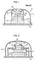
- Fig. 1 shows a simplified cross-sectional view of a thermoelectrically cooled detector assembly 10 of the prior art.
- Assembly 10 includes a backplate or chassis 12 to which are mounted a dewar vacuum shell 14 and a six stage (1-6) thermoelectric cooler 16.
- Mounted to the sixth and coldest stage of the cooler 16 is an IR radiation detector chip 18 having an associated substrate 20 and hookup wiring 22.
- Electrical cabling 24 couples the detector 18 to associated electronics (not shown).
- coldshield 26 having an aperture 28 defining a coldstop is mounted to the second stage of the cooler 16 and is cooled thereby.
- a dewar window 30 is positioned relative to the aperture 28 to admit IR radiation into the assembly 10 for viewing by the detector 18.
- the sixth stage of the cooler 20 and detector 18 mounted thereupon typically attains a coldest temperature of approximately 185 K under ambient temperature conditions of 323 K (+50°C), although the exact temperature is not critical to this invention.
- the cooler 16 has a shape defined by larger, higher temperature stages positioned beneath smaller, lower temperature stages. The resulting somewhat conical shape of the cooler 16 is exploited by the radiation shield of the invention as will be described below.
- the coldshield 26 is not required to be mounted to the coldest stage of the cooler 18 in that thermal, as opposed to photon noise, dominates detector performance at 185 K operating temperatures. If the coldshield 26 were cooled further by mounting it to the coldest stage, only an insignificant reduction in detector 18 background flux would occur while radiative transfer into the coldshield would be conducted directly to the coldest stage increasing coldest-stage heatloads, thereby raising the detector 18 temperature and degrading performance. Furthermore, mounting the coldshield 18 to the coldest cooler stage would detrimentally reduce the ruggedness of the assembly 10.
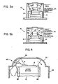
- Fig. 2 there is shown a simplified view of the assembly 10 of Fig. 1 wherein the coldshield 26 is replaced by the uncooled radiation shield 40 of the invention.
- the shield 40 is mounted via mounting apparatus 41 to the outer case of the assembly 10 and is not affixed to any part of cooler 18.
- the shield 40 has a curved reflective upper surface 42 having the shape of a toric segment and circular cylindrical or rectangular parallelepiped reflective sidewalls 46 for imaging the detector 18 and the upper cooler stage upon the tops and sides of lower and warmer cooler stages. This beneficially reduces the heatload upon the coldest stage by excluding warmer surfaces from its view.
- An aperture 46 defines the effective coldstop for the detector 18.
- the shield 40 of the invention exploits an important optical characteristic of toric reflectors, that is, toric reflectors image a point into a focussed annular region which surrounds the point. Therefore points of the detector 18 and the coldest cooler stage are imaged into rings surrounding the detector and the coldest stage. In accordance with the invention, the rings are further imaged beyond the edge of the detector 18 and the coldest stage of the cooler and eventually upon cooled absorptive surface(s) 52b below the detector and coldest stage.
- toric reflectors overcomes several problems associated with many conventional reflectors that image points to points; that is, total ray blockage does not occur when reflective obstructions such as cabling lie within the imaged ring, and also ghost imaging and optical crosstalk are not generated in that reflections from points of the detector 18 are not imaged back upon the detector.
- the toric shape of the reflector 42 is generated by placing the surface generating point A on or near the edge of detector 18. This orients the toric surface of reflector 42 for reflecting rays B behind the detector 18 and to the warmer and larger cooler 16 stages. Any ray from the detector 18 is reflected away from the detector since the angle of reflection from the toric surface is equal and opposite to the angle of incidence, these angles being measured with respect to the reflector 42 surface normal which approximately intercepts the edge of the detector.
- the optimization of the shape and placement of reflector 42 is preferably achieved through known optical ray tracing techniques in order to achieve the lowest flux reflections upon the coldest cooler stage.
- Another feature of the invention is the containment of energy within distinct zones of similar temperature. This provides that, even if rays strike reflective surfaces such as wiring, the rays are re-reflected by the reflective sidewalls 44 of the radiation shield until the rays strike an absorbing surface.
- the upper side surfaces of the cooler 16 are enclosed within an optically reflective and thermally insulating sheath 48.
- One suitable material for the sheath 48 is a gold-plated polyimide plastic of a type commonly used in fine-line electronics cables.
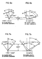
- the single toric segment reflector 42 is readily fabricated as are the lower cylindrical or rectangular reflector segments. If desired, and as shown in Fig. 3a, a lower toric reflector 50 can be provided to direct rays more inwardly and towards the intermediate temperature stages. Furthermore, and as shown in Fig. 3b and Fig. 2, for many applications it may be preferable to cause the shield 40 to closely follow or fit the shape of the cooler 16. For some applications where additional height is desired multiple toric reflectors can be provided further from the detector 18 than primary toric shield 42, in a manner as shown in U.S. Patent No. 4,820,923, in order to direct energy across the central volume of the assembly 10 to avoid interference with the lower toric shield.
- thermoelectric cooler 16 stages are provided with one or more extensions 52 to their thermally conductive plates in order to better control radiative transfer.
- the lower surface 52a of each plate 52 is preferably plated or otherwise treated to increase reflectance and decrease absorptance while the upper surface 52b is treated to be absorptive for viewing by the reflective shield, thereby effectively forming an exit aperture for disposing of energy that otherwise might be reflected back to the coldest stage.
- the side surfaces of the upper cooler stage(s) are sheathed and at least in part made reflective, as noted above, to augment imaging upon the lower absorptive areas, thereby improving this desirable absorption of unwanted energy.
- Another desirable effect is to prevent the intermediate temperature cooler stages from viewing hotter or case-temperature surfaces; instead these intermediate stages are reimaged upon themselves or upon stages which are only slightly warmer than themselves.
- the cooler 16 is modeled as shown in Fig. 5, and includes typical temperatures and surface areas at each stage.
- the model represents a typical six stage thermoelectric cooler that attains a coldest stage temperature of approximately 185 K under worst case ambient conditions of +50°C.
- the cooler model considers both lateral and vertical surface areas. For each stage the surface area excludes the "footprint" of an overlying stage and includes the areas of above and below half-sides.
- the topmost cooler stage is assumed to have a circular cylindrical shape with a diameter of 7.5 mm.
- the cooler stage heights are 2.0 mm and the stage lateral dimensions are taken as increasing in the ratio of 1.5:1 at every other stage. Rectangular or square shapes of the same areas would yield similar results.
- the upper stage absorption is taken to be 50% (0.5 W/W) which allows for reflective gold wiring over half the surface of otherwise absorptive materials such as ceramic, adhesive, Si or HgCdTe.
- the effective upper stage area is 0.9 cm2.
- the conventional true coldshield 26 is mounted upon the second stage of the cooler 16.
- the heatload of the coldshield is minimized by gold-plating the shield exterior to reduce absorption.
- this heatload causes some rise in shield temperature, for example, approximately 20°C to a coldshield temperature of 297 K.
- This heat rise is critical if the coldshield interior is blackened, hence capable of emitting significant flux.
- radiant emittance is 44 mW/cm2 over the full spectral band. Because the shield 26 surrounds the cold stage it can be shown that a flux of 44 mW/cm2 x 0.9 cm2 x 0.5 W/W, or approximately 20 mW, is incident upon the coldest stage.
- the coldshield 26 interior is reflective, not blackened, there is an apparent emittance because the shield reflects objects that it encloses. This can be considered a diffuse emittance for it is due to reflections not having any coherent imaging.
- the equivalent shield temperature can be cooler than the actual temperature for it is both an area-weighted and an emittance-weighted average of objects within the cavity.
- the radiant emittance is 25 mW/cm2 over the full spectral band and a flux of 25 mW/cm2 x 0.9 cm2 x 0.97 x 0.5 W/W, or approximately 11mW, is incident upon the coldest stage.
- direct radiance upon the coldest stage is 44 mW/cm2 x 0.5 W/W x 0.9 cm2 x 0.03, or approximately 1 mW.
- the coldstop 28 subtends a solid angle of approximately 1.7 steradians. Through it, energy within the dewar also is reflected upon the detector 18 in that the stop is placed well below the bandpass filter of window 30. This is because the window 30 and coldshield exterior are reflective and because the geometry allows substantial reflections of warm objects within the dewar, such as the dewar case and base.
- the direct radiance upon the upper cooler stage from objects at 323 K ambient temperature is 0.7 x 1.7/pi x 62 mW/cm2 x 0.9 cm2 x 0.5 W/W, or approximately 10 mW.
- the total radiative heatload on the coldest stage of cooler 16 can be estimated to be (11 + 1 + 10) or approximately 22 mW.
- the detector 18 would be surrounded by 323 K radiation and would receive 62 mW/cm2 x 0.9 cm2 x 0.5 W/W, or approximately of 28 mW of flux.
- the conventional coldshield has reduced the unwanted flux by approximately 6 mW.
- this conventional coldshield 26 reduces detector 18 temperatures by approximately 2°C as compared with an unshielded design.
- the detector 18 sees no temperatures warmer than the 231 K of cooler stage 4, thus it experiences a reflected heatload from the shield of less than 16 mW/cm2 x 0.97 x 0.9 cm2 x 0.5 W/W, or approximately 7 mW.
- Thermal conduction from the above-described reflective sheath 48 involves a series path, through the supporting material as well as along the reflective film. It can be shown that the thermal conductivity of a gold film, 700 angstroms thick, 0.24 cm wide, and 0.2 cm long, is approximately 3000 mW/cm K x (1/0.2 cm) x 0.24 cm x 700 angstroms x 10 ⁇ 8cm/angstroms, or approximately 0.025 mW/K. Conductivity of the supporting polyimide plastic film, 0.004-inch thick, perfectly contacting a cooler 16 stage edge area of 0.05 cm x 0.24 cm is 1.2 mW/K x (1/0.01 cm) x 0.05 cm x 0.24 cm, or approximately 1 mW/K.
- thermal conduction through the sheath 48 certainly is no greater than that of the gold film alone. Therefore, with or without the supporting thermally insulating sheath, gold plating of the upper stage sides adds a negligible heatload of 0.025 mW/K x 46 K or approximately 1 mW, which is far less than the radiative load that would be incurred without plating. It should be noted that plating or sheathing of the cooler 16 sides was consistently considered into the overall coldest-stage absorption of 50% employed in all calculations.
- Some unwanted flux results from the non-zero emissivity and warm temperature of the reflector 40.
- the cold stage experiences an added radiative heatload of 62 mW/cm2 x 0.03 W/W x 0.9 cm2 x 0.5 W/W or approximately 1 mW.
- This lower detector operating temperature improves minimum detectable signal by 5%, based upon typical photovoltaic mercury-cadmium-telluride detector characteristics, and is realized solely by employing the radiation shield of the invention.
- shield design can now be modified other improvements also can be made, as are shown below.
- the heatload due to coldstage reflections by the shield will increase from 7 mW to 33 mW/cm2 x 0.97 x 0.8 cm2 x 0.5 W/W or approximately 14 mW, but other heatloads will remain the same.
- detector temperature will increase by approximately 2.3°C, and minimum detectable signal will be degraded by 9%, relative to the better performance design previously described, again without changing the coldstop location.
- This variation degrades minimum detectable signal by 4% as compared with the prior art exemplary baseline, but still offers improved ruggedness of construction and other advantages of this invention.
- the placement and the concave shape of the conventional coldshield front surface shown in Fig. 1 are chosen to avoid some undesirable system-optics imaging effects.
- the relatively short height above the detector 18 also avoids placing a large cantilevered mass upon the cooler 16, thereby avoiding structural problems due to the fragility of the cooler 16.
- the shield exterior can be made absorptive or diffusely reflecting, and still achieve acceptable rejection of images.
- the shield 40 can be made large and/or massive without posing structural design problems. Therefore, other shapes become feasible such that the aperture 46 can be placed nearer to the window 30. This reduces detector background flux significantly.
- the conventional stop is only a few detector dimensions above the detector 18 surface, hence the stop is oversized to avoid vignetting.
- the stop is made effectively F/0.2 in the long array dimension, and F/0.7 in the short dimension.
- the imaging ray bundle is contained within an F/1.5 cone, except for effects of pupil wander, and the conventional stop admits only an F/1.1 (24° half-angle cone) without vignetting. Due to its proximity to the detector 18, the conventional stop subtends a large solid angle of approximately 1.7 steradians.
- Figs. 7a and 7b If, without changing the dewar envelope, the stop is placed as shown in Figs. 7a and 7b, a better fit is achieved to the system focal number.
- This stop at 0.200-inch height, is approximately F/0.6 by F/1.0, and subtends an equivalent solid angle of approximately 1.0 steradian. It might be inferred that the radiation through the coldstop will be reduced to 1/1.7 or approximately 0.6 of the conventional value. However, a larger improvement results, since the closer spacing to the window 30 inhibits energy emitted by warm surfaces within the dewar from reaching the coldest stage through window reflections.
- window reflections generally include large amounts of LWIR flux which are well reflected by the MWIR filter coatings typically applied to window 30.
- the previously described reflection-coupling efficiency of 70% is reduced to less than 5%.
- This 9 mW/cm2 heatload reduction reduces detector operating temperature another 3K.
- detector photon noise depends upon the radiation within the detector sensitive spectral band.
- the foregoing radiometric analyses quantify the performance advantages of the radiation shield of the invention and of improvements that it enables in coldstop placement.
- the improved detector-cooler-dewar unit achieves a minimum detectable signal improvement of approximately 15%, together with better producibility and reliability.
- thermoelectrically-cooled infrared detector While the above description has been made in the context of a specific embodiment of a thermoelectrically-cooled infrared detector, it is clear that other cryogenically-cooled components can benefit these teachings.
- a magnetic or nuclear radiation sensor may require no coldstop aperture inasmuch as the entire radiation shield can be transparent to the energy being sensed.
- the technique also works in reverse for infrared or thermal objects that are to be viewed by external sensing systems.
- the teaching of the invention is applicable to the construction of calibration targets for thermal imaging systems.
Landscapes
- Physics & Mathematics (AREA)
- Engineering & Computer Science (AREA)
- General Physics & Mathematics (AREA)
- Spectroscopy & Molecular Physics (AREA)
- Mechanical Engineering (AREA)
- Thermal Sciences (AREA)
- General Engineering & Computer Science (AREA)
- Photometry And Measurement Of Optical Pulse Characteristics (AREA)
- Radiation Pyrometers (AREA)
Applications Claiming Priority (2)
| Application Number | Priority Date | Filing Date | Title |
|---|---|---|---|
| US07/370,556 US4990782A (en) | 1989-06-23 | 1989-06-23 | Radiation shield for thermoelectrically cooled infrared detectors |
| US370556 | 1989-06-23 |
Publications (3)
| Publication Number | Publication Date |
|---|---|
| EP0403880A2 true EP0403880A2 (de) | 1990-12-27 |
| EP0403880A3 EP0403880A3 (de) | 1991-02-06 |
| EP0403880B1 EP0403880B1 (de) | 1996-08-14 |
Family
ID=23460178
Family Applications (1)
| Application Number | Title | Priority Date | Filing Date |
|---|---|---|---|
| EP90110714A Expired - Lifetime EP0403880B1 (de) | 1989-06-23 | 1990-06-06 | Strahlungsabschirmung für thermoelektrisch gekühlte Infrarotdetektoren |
Country Status (5)
| Country | Link |
|---|---|
| US (1) | US4990782A (de) |
| EP (1) | EP0403880B1 (de) |
| JP (1) | JPH0731081B2 (de) |
| DE (1) | DE69028046T2 (de) |
| IL (1) | IL94440A0 (de) |
Cited By (5)
| Publication number | Priority date | Publication date | Assignee | Title |
|---|---|---|---|---|
| WO1994018530A1 (de) * | 1993-02-04 | 1994-08-18 | Steinheil Optronik Gmbh | Infrarot-strahlendetektoreinrichtung |
| EP0646972A3 (de) * | 1993-10-01 | 1995-04-19 | Texas Instruments Incorporated | Verbesserungen von oder bezüglich auf Detektoranordnungen |
| DE19522444A1 (de) * | 1995-01-24 | 1996-01-25 | Walz Heinz Gmbh | Tragbare Gaswechselkammer |
| RU2149365C1 (ru) * | 1998-07-16 | 2000-05-20 | Закрытое акционерное общество "Матричные технологии" | Приемник ик излучения |
| US11946598B2 (en) | 2018-09-12 | 2024-04-02 | The Regents of of the University of Colorado, a body corporate | Cryogenically cooled vacuum chamber radiation shields for ultra-low temperature experiments and extreme high vacuum (XHV) conditions |
Families Citing this family (33)
| Publication number | Priority date | Publication date | Assignee | Title |
|---|---|---|---|---|
| JP2977829B2 (ja) * | 1989-01-11 | 1999-11-15 | 株式会社東芝 | 動画像再生装置および動画像再生方法 |
| US5128796A (en) * | 1989-03-31 | 1992-07-07 | The United States Of America As Represented By The Administrator Of The National Aeronautics And Space Administration | Cryogenic shutter |
| US5089705A (en) * | 1990-02-16 | 1992-02-18 | Fujitsu Limited | Infrared detector having dewar with film coatings to suppress reflections |
| US5081358A (en) * | 1990-02-23 | 1992-01-14 | Shimadzu Corporation | Detector of fourier transform infrared spectrometer |
| US5298752A (en) * | 1992-09-30 | 1994-03-29 | Loral Fairchild Corporation | Retroreflectors for increasing cold shield efficiency |
| DE4327656A1 (de) * | 1993-08-17 | 1995-02-23 | Steinheil Optronik Gmbh | Infrarot-Objektiv |
| US5444250A (en) * | 1994-08-15 | 1995-08-22 | Hughes Aircraft Company | Optical warm stop with fresnel type reflective surface |
| FR2738355B1 (fr) * | 1995-08-28 | 1997-10-31 | Aerospatiale | Piege a lumiere |
| US5763885A (en) * | 1995-12-19 | 1998-06-09 | Loral Infrared & Imaging Systems, Inc. | Method and apparatus for thermal gradient stabilization of microbolometer focal plane arrays |
| US6318035B1 (en) | 1999-06-01 | 2001-11-20 | Lockheed Martin Corporation | Window frame assembly for use in an aircraft and associated method of manufacture |
| US6396061B1 (en) * | 1999-09-24 | 2002-05-28 | The Regents Of The University Of California | Actively driven thermal radiation shield |
| US6610984B2 (en) | 2000-03-17 | 2003-08-26 | Infrared Components Corporation | Method and apparatus for correction of microbolometer output |
| US6630674B2 (en) | 2000-03-17 | 2003-10-07 | Infrared Components Corporation | Method and apparatus for correction of microbolometer output |
| US6596997B2 (en) * | 2001-08-03 | 2003-07-22 | Irvine Sensors Corporation | Retro-reflector warm stop for uncooled thermal imaging cameras and method of using the same |
| US20040065850A1 (en) * | 2002-10-02 | 2004-04-08 | Kane Todd A. | Thermal imaging identification signage |
| US7002154B2 (en) * | 2003-04-25 | 2006-02-21 | Raytheon Company | Optical system for a wide field of view staring infrared sensor having improved optical symmetry |
| DE10325906B4 (de) * | 2003-06-05 | 2007-03-15 | Erwin Martin Heberer | Vorrichtung zur Abschirmung von kohärenter elektromagnetischer Strahlung sowie Laserkabine mit einer solchen Vorrichtung |
| US20050245364A1 (en) * | 2004-04-30 | 2005-11-03 | Juliu Horvath | Exercise device |
| DE102004028022B4 (de) * | 2004-06-09 | 2006-11-16 | Perkinelmer Optoelectronics Gmbh & Co.Kg | Sensor |
| US6969840B1 (en) | 2004-08-02 | 2005-11-29 | Raytheon Company | Imaging optical system including a telescope and an uncooled warm-stop structure |
| US7180067B2 (en) * | 2005-02-15 | 2007-02-20 | Raytheon Company | Infrared imaging system with ellipsoid reflective warm baffle and method |
| US8516834B2 (en) | 2008-08-14 | 2013-08-27 | S2 Corporation | Apparatus and methods for improving vibration isolation, thermal dampening, and optical access in cryogenic refrigerators |
| JP5225829B2 (ja) * | 2008-12-24 | 2013-07-03 | 浜松ホトニクス株式会社 | 分光測定装置 |
| JP5221322B2 (ja) * | 2008-12-24 | 2013-06-26 | 浜松ホトニクス株式会社 | 分光測定装置及びデュワ |
| US9157806B2 (en) * | 2010-02-18 | 2015-10-13 | Rafael Advanced Defense Systems Ltd. | System and method for changing spectral range of a cryogenically cooled detector |
| JP4637274B1 (ja) * | 2010-07-06 | 2011-02-23 | 株式会社光文書院 | 算数教習具 |
| WO2012049683A1 (en) * | 2010-10-14 | 2012-04-19 | Semi Conductor Devices-Elbit Systems-Rafael Partnership | Dewar assembly for ir detection systems |
| JP6706522B2 (ja) * | 2016-03-25 | 2020-06-10 | 株式会社日立ハイテクサイエンス | 試料容器及び熱分析装置 |
| US10753805B2 (en) | 2017-04-05 | 2020-08-25 | Kaiser Optical Systems Inc. | Radiation shield for near-infrared detectors |
| US10190907B1 (en) * | 2017-09-29 | 2019-01-29 | Raytheon Company | Convex warm shield for thermal imaging device |
| CN111405147B (zh) * | 2019-01-02 | 2021-12-07 | 三赢科技(深圳)有限公司 | 镜头模组及电子装置 |
| CN111403504B (zh) * | 2020-03-23 | 2023-06-02 | 长春长光奥闰光电科技有限公司 | 一种大靶面探测器阵列式多级半导体制冷方法 |
| US20220123161A1 (en) * | 2020-10-21 | 2022-04-21 | University Of Iowa Research Foundation | Cascaded type ii superlattice infrared detector operating at 300 k |
Family Cites Families (12)
| Publication number | Priority date | Publication date | Assignee | Title |
|---|---|---|---|---|
| US2738700A (en) * | 1949-06-20 | 1956-03-20 | Northrop Aircraft Inc | Glare-stopped optical system |
| US3445659A (en) * | 1967-01-09 | 1969-05-20 | Philco Ford Corp | Cryogenically cooled radiation detection apparatus |
| US3648056A (en) * | 1970-01-12 | 1972-03-07 | Honeywell Inc | Optical detector with radiant energy absorbing chamber |
| SU495633A1 (ru) * | 1972-11-27 | 1975-12-15 | Оптическа система | |
| US4217026A (en) * | 1978-08-25 | 1980-08-12 | The United States Of America As Represented By The Secretary Of The Air Force | Elliptic cylindrical baffle assembly |
| US4339748A (en) * | 1980-04-08 | 1982-07-13 | American District Telegraph Company | Multiple range passive infrared detection system |
| US4431917A (en) * | 1981-11-27 | 1984-02-14 | Texas Instruments Incorporated | Compact, high cold shield efficiency optical system |
| GB2115143B (en) * | 1982-02-17 | 1985-09-25 | British Aerospace | Infra-red radiation detector assembly |
| US4507551A (en) * | 1983-03-14 | 1985-03-26 | Honeywell Inc. | Optical detection system having a detector lens comprising a rear landscape lens |
| US4542963A (en) * | 1984-03-28 | 1985-09-24 | The United States Of America As Represented By The United States National Aeronautics And Space Administration | Optical system with reflective baffles |
| US4820923A (en) * | 1986-06-19 | 1989-04-11 | Santa Barbara Research Center | Uncooled reflective shield for cryogenically-cooled radiation detectors |
| DE3716358A1 (de) * | 1987-05-15 | 1988-12-01 | Steinheil Optronik Gmbh | Infrarot-strahlungsdetektor |
-
1989
- 1989-06-23 US US07/370,556 patent/US4990782A/en not_active Expired - Fee Related
-
1990
- 1990-05-18 IL IL94440A patent/IL94440A0/xx not_active IP Right Cessation
- 1990-06-06 DE DE69028046T patent/DE69028046T2/de not_active Expired - Fee Related
- 1990-06-06 EP EP90110714A patent/EP0403880B1/de not_active Expired - Lifetime
- 1990-06-22 JP JP2163016A patent/JPH0731081B2/ja not_active Expired - Fee Related
Cited By (6)
| Publication number | Priority date | Publication date | Assignee | Title |
|---|---|---|---|---|
| WO1994018530A1 (de) * | 1993-02-04 | 1994-08-18 | Steinheil Optronik Gmbh | Infrarot-strahlendetektoreinrichtung |
| US6057550A (en) * | 1993-02-04 | 2000-05-02 | Steinheil Optronik Gmbh | Infrared objective |
| EP0646972A3 (de) * | 1993-10-01 | 1995-04-19 | Texas Instruments Incorporated | Verbesserungen von oder bezüglich auf Detektoranordnungen |
| DE19522444A1 (de) * | 1995-01-24 | 1996-01-25 | Walz Heinz Gmbh | Tragbare Gaswechselkammer |
| RU2149365C1 (ru) * | 1998-07-16 | 2000-05-20 | Закрытое акционерное общество "Матричные технологии" | Приемник ик излучения |
| US11946598B2 (en) | 2018-09-12 | 2024-04-02 | The Regents of of the University of Colorado, a body corporate | Cryogenically cooled vacuum chamber radiation shields for ultra-low temperature experiments and extreme high vacuum (XHV) conditions |
Also Published As
| Publication number | Publication date |
|---|---|
| US4990782A (en) | 1991-02-05 |
| JPH0731081B2 (ja) | 1995-04-10 |
| JPH03142330A (ja) | 1991-06-18 |
| DE69028046D1 (de) | 1996-09-19 |
| DE69028046T2 (de) | 1997-03-20 |
| IL94440A0 (en) | 1991-03-10 |
| EP0403880B1 (de) | 1996-08-14 |
| EP0403880A3 (de) | 1991-02-06 |
Similar Documents
| Publication | Publication Date | Title |
|---|---|---|
| EP0403880B1 (de) | Strahlungsabschirmung für thermoelektrisch gekühlte Infrarotdetektoren | |
| US4754139A (en) | Uncooled high resolution infrared imaging plane | |
| US5371369A (en) | Conformal cold baffle for optical imaging systems | |
| JP3839487B2 (ja) | デュアルバンドマルチレベルマイクロブリッジ検出器 | |
| US7262412B2 (en) | Optically blocked reference pixels for focal plane arrays | |
| US3963926A (en) | Detector cold shield | |
| US4937450A (en) | Infrared detector comprising an evacuated and cooled Dewar having an elliptical spheroid end window | |
| EP1060370B1 (de) | Verfahren und vorrichtung zum messen der substrattemperatur | |
| AU1866595A (en) | Noncontact active temperature sensor | |
| WO1997021250A1 (en) | Infrared radiation detector having a reduced active area | |
| US5075553A (en) | IR sensor for a scanned staggered element linear array having improved cold shielding | |
| EP1709406B1 (de) | Thermisch stabilisierter strahlungsdetektor mit temperaturgeregeltem strahlungsfilter | |
| EP0646972A2 (de) | Verbesserungen von oder bezüglich auf Detektoranordnungen | |
| US5408100A (en) | Chromatic radiance attenuator | |
| US5260575A (en) | Infrared detector | |
| US5021657A (en) | Thermal imager | |
| US6091069A (en) | Infrared optical system | |
| US5525801A (en) | Two-color photo-conductive linear detector | |
| US6677588B1 (en) | Detector assembly having reduced stray light ghosting sensitivity | |
| US5017786A (en) | V2 O3 protection for IR detector arrays against intense thermal radiation | |
| US4987305A (en) | Infra-red sensing system | |
| US5485005A (en) | Cooled x-ray sensitive photoconductor | |
| Swift | Performance of background-limited systems for space use | |
| EP0412646A2 (de) | Reflexionseinrichtung für Infrarotdetektoren | |
| US3163760A (en) | Refractive optics infrared scanning system |
Legal Events
| Date | Code | Title | Description |
|---|---|---|---|
| PUAI | Public reference made under article 153(3) epc to a published international application that has entered the european phase |
Free format text: ORIGINAL CODE: 0009012 |
|
| PUAL | Search report despatched |
Free format text: ORIGINAL CODE: 0009013 |
|
| AK | Designated contracting states |
Kind code of ref document: A2 Designated state(s): DE FR GB IT NL |
|
| AK | Designated contracting states |
Kind code of ref document: A3 Designated state(s): DE FR GB IT NL |
|
| 17P | Request for examination filed |
Effective date: 19910708 |
|
| 17Q | First examination report despatched |
Effective date: 19920727 |
|
| GRAH | Despatch of communication of intention to grant a patent |
Free format text: ORIGINAL CODE: EPIDOS IGRA |
|
| GRAH | Despatch of communication of intention to grant a patent |
Free format text: ORIGINAL CODE: EPIDOS IGRA |
|
| GRAA | (expected) grant |
Free format text: ORIGINAL CODE: 0009210 |
|
| AK | Designated contracting states |
Kind code of ref document: B1 Designated state(s): DE FR GB IT NL |
|
| REF | Corresponds to: |
Ref document number: 69028046 Country of ref document: DE Date of ref document: 19960919 |
|
| ET | Fr: translation filed | ||
| ITF | It: translation for a ep patent filed | ||
| PLBE | No opposition filed within time limit |
Free format text: ORIGINAL CODE: 0009261 |
|
| STAA | Information on the status of an ep patent application or granted ep patent |
Free format text: STATUS: NO OPPOSITION FILED WITHIN TIME LIMIT |
|
| 26N | No opposition filed | ||
| REG | Reference to a national code |
Ref country code: GB Ref legal event code: 732E |
|
| NLS | Nl: assignments of ep-patents |
Owner name: RAYTHEON COMPANY;HUGHES AIRCRAFT COMPANY;HE HOLDIN |
|
| REG | Reference to a national code |
Ref country code: FR Ref legal event code: TP Ref country code: FR Ref legal event code: CD Ref country code: FR Ref legal event code: CA |
|
| REG | Reference to a national code |
Ref country code: GB Ref legal event code: IF02 |
|
| PGFP | Annual fee paid to national office [announced via postgrant information from national office to epo] |
Ref country code: FR Payment date: 20060511 Year of fee payment: 17 |
|
| PGFP | Annual fee paid to national office [announced via postgrant information from national office to epo] |
Ref country code: NL Payment date: 20060515 Year of fee payment: 17 |
|
| PGFP | Annual fee paid to national office [announced via postgrant information from national office to epo] |
Ref country code: GB Payment date: 20060516 Year of fee payment: 17 |
|
| PGFP | Annual fee paid to national office [announced via postgrant information from national office to epo] |
Ref country code: DE Payment date: 20060523 Year of fee payment: 17 |
|
| PGFP | Annual fee paid to national office [announced via postgrant information from national office to epo] |
Ref country code: IT Payment date: 20060630 Year of fee payment: 17 |
|
| GBPC | Gb: european patent ceased through non-payment of renewal fee |
Effective date: 20070606 |
|
| NLV4 | Nl: lapsed or anulled due to non-payment of the annual fee |
Effective date: 20080101 |
|
| REG | Reference to a national code |
Ref country code: FR Ref legal event code: ST Effective date: 20080229 |
|
| PG25 | Lapsed in a contracting state [announced via postgrant information from national office to epo] |
Ref country code: NL Free format text: LAPSE BECAUSE OF NON-PAYMENT OF DUE FEES Effective date: 20080101 Ref country code: DE Free format text: LAPSE BECAUSE OF NON-PAYMENT OF DUE FEES Effective date: 20080101 |
|
| PG25 | Lapsed in a contracting state [announced via postgrant information from national office to epo] |
Ref country code: GB Free format text: LAPSE BECAUSE OF NON-PAYMENT OF DUE FEES Effective date: 20070606 |
|
| PG25 | Lapsed in a contracting state [announced via postgrant information from national office to epo] |
Ref country code: FR Free format text: LAPSE BECAUSE OF NON-PAYMENT OF DUE FEES Effective date: 20070702 |
|
| PG25 | Lapsed in a contracting state [announced via postgrant information from national office to epo] |
Ref country code: IT Free format text: LAPSE BECAUSE OF NON-PAYMENT OF DUE FEES Effective date: 20070606 |