EP0404080A2 - Schaltung zur Speisung einer externen Schaltung und eines Vorteilers mit einem Oszillatorsignal - Google Patents
Schaltung zur Speisung einer externen Schaltung und eines Vorteilers mit einem Oszillatorsignal Download PDFInfo
- Publication number
- EP0404080A2 EP0404080A2 EP90111596A EP90111596A EP0404080A2 EP 0404080 A2 EP0404080 A2 EP 0404080A2 EP 90111596 A EP90111596 A EP 90111596A EP 90111596 A EP90111596 A EP 90111596A EP 0404080 A2 EP0404080 A2 EP 0404080A2
- Authority
- EP
- European Patent Office
- Prior art keywords
- transistor
- oscillator
- transistors
- base
- power supply
- Prior art date
- Legal status (The legal status is an assumption and is not a legal conclusion. Google has not performed a legal analysis and makes no representation as to the accuracy of the status listed.)
- Granted
Links
Images


Classifications
-
- H—ELECTRICITY
- H03—ELECTRONIC CIRCUITRY
- H03B—GENERATION OF OSCILLATIONS, DIRECTLY OR BY FREQUENCY-CHANGING, BY CIRCUITS EMPLOYING ACTIVE ELEMENTS WHICH OPERATE IN A NON-SWITCHING MANNER; GENERATION OF NOISE BY SUCH CIRCUITS
- H03B5/00—Generation of oscillations using amplifier with regenerative feedback from output to input
- H03B5/08—Generation of oscillations using amplifier with regenerative feedback from output to input with frequency-determining element comprising lumped inductance and capacitance
- H03B5/12—Generation of oscillations using amplifier with regenerative feedback from output to input with frequency-determining element comprising lumped inductance and capacitance active element in amplifier being semiconductor device
- H03B5/1231—Generation of oscillations using amplifier with regenerative feedback from output to input with frequency-determining element comprising lumped inductance and capacitance active element in amplifier being semiconductor device the amplifier comprising one or more bipolar transistors
-
- H—ELECTRICITY
- H03—ELECTRONIC CIRCUITRY
- H03B—GENERATION OF OSCILLATIONS, DIRECTLY OR BY FREQUENCY-CHANGING, BY CIRCUITS EMPLOYING ACTIVE ELEMENTS WHICH OPERATE IN A NON-SWITCHING MANNER; GENERATION OF NOISE BY SUCH CIRCUITS
- H03B5/00—Generation of oscillations using amplifier with regenerative feedback from output to input
- H03B5/08—Generation of oscillations using amplifier with regenerative feedback from output to input with frequency-determining element comprising lumped inductance and capacitance
- H03B5/12—Generation of oscillations using amplifier with regenerative feedback from output to input with frequency-determining element comprising lumped inductance and capacitance active element in amplifier being semiconductor device
- H03B5/1206—Generation of oscillations using amplifier with regenerative feedback from output to input with frequency-determining element comprising lumped inductance and capacitance active element in amplifier being semiconductor device using multiple transistors for amplification
- H03B5/1212—Generation of oscillations using amplifier with regenerative feedback from output to input with frequency-determining element comprising lumped inductance and capacitance active element in amplifier being semiconductor device using multiple transistors for amplification the amplifier comprising a pair of transistors, wherein an output terminal of each being connected to an input terminal of the other, e.g. a cross coupled pair
- H03B5/1215—Generation of oscillations using amplifier with regenerative feedback from output to input with frequency-determining element comprising lumped inductance and capacitance active element in amplifier being semiconductor device using multiple transistors for amplification the amplifier comprising a pair of transistors, wherein an output terminal of each being connected to an input terminal of the other, e.g. a cross coupled pair the current source or degeneration circuit being in common to both transistors of the pair, e.g. a cross-coupled long-tailed pair
-
- H—ELECTRICITY
- H03—ELECTRONIC CIRCUITRY
- H03B—GENERATION OF OSCILLATIONS, DIRECTLY OR BY FREQUENCY-CHANGING, BY CIRCUITS EMPLOYING ACTIVE ELEMENTS WHICH OPERATE IN A NON-SWITCHING MANNER; GENERATION OF NOISE BY SUCH CIRCUITS
- H03B5/00—Generation of oscillations using amplifier with regenerative feedback from output to input
- H03B5/08—Generation of oscillations using amplifier with regenerative feedback from output to input with frequency-determining element comprising lumped inductance and capacitance
- H03B5/12—Generation of oscillations using amplifier with regenerative feedback from output to input with frequency-determining element comprising lumped inductance and capacitance active element in amplifier being semiconductor device
- H03B5/1237—Generation of oscillations using amplifier with regenerative feedback from output to input with frequency-determining element comprising lumped inductance and capacitance active element in amplifier being semiconductor device comprising means for varying the frequency of the generator
- H03B5/1271—Generation of oscillations using amplifier with regenerative feedback from output to input with frequency-determining element comprising lumped inductance and capacitance active element in amplifier being semiconductor device comprising means for varying the frequency of the generator the frequency being controlled by a control current, i.e. current controlled oscillators
-
- H—ELECTRICITY
- H03—ELECTRONIC CIRCUITRY
- H03B—GENERATION OF OSCILLATIONS, DIRECTLY OR BY FREQUENCY-CHANGING, BY CIRCUITS EMPLOYING ACTIVE ELEMENTS WHICH OPERATE IN A NON-SWITCHING MANNER; GENERATION OF NOISE BY SUCH CIRCUITS
- H03B2200/00—Indexing scheme relating to details of oscillators covered by H03B
- H03B2200/003—Circuit elements of oscillators
- H03B2200/0034—Circuit elements of oscillators including a buffer amplifier
-
- H—ELECTRICITY
- H03—ELECTRONIC CIRCUITRY
- H03B—GENERATION OF OSCILLATIONS, DIRECTLY OR BY FREQUENCY-CHANGING, BY CIRCUITS EMPLOYING ACTIVE ELEMENTS WHICH OPERATE IN A NON-SWITCHING MANNER; GENERATION OF NOISE BY SUCH CIRCUITS
- H03B2200/00—Indexing scheme relating to details of oscillators covered by H03B
- H03B2200/006—Functional aspects of oscillators
- H03B2200/0098—Functional aspects of oscillators having a balanced output signal
-
- H—ELECTRICITY
- H03—ELECTRONIC CIRCUITRY
- H03B—GENERATION OF OSCILLATIONS, DIRECTLY OR BY FREQUENCY-CHANGING, BY CIRCUITS EMPLOYING ACTIVE ELEMENTS WHICH OPERATE IN A NON-SWITCHING MANNER; GENERATION OF NOISE BY SUCH CIRCUITS
- H03B5/00—Generation of oscillations using amplifier with regenerative feedback from output to input
- H03B5/02—Details
- H03B5/04—Modifications of generator to compensate for variations in physical values, e.g. power supply, load, temperature
Definitions
- This invention relates to an oscillator usable in various apparatuses such as mobile radio communication equipments.
- a good way of miniaturizing an oscillator is to form at least part of the oscillator by an integrated circuit (IC).
- IC integrated circuit
- Japanese published unexamined patent application 64-8704 discloses an oscillator designed to be formed by an IC.
- a power supply voltage is directly applied to the collectors of transistors, so that the amplitude of an oscillator output vibrates around the power supply voltage and an RF oscillator signal tends to leak toward the potter supply.
- the base bias voltages can not be freely set to optimal values which are determined from the standpoint of a C/N ratio (a carrier-to-noise ratio).
- the base voltages and the collector voltages fluctuate with variations in the power supply voltage, so that the C/N ratio tends to be lowered by the variations in the power supply voltage.
- an oscillator comprises first and second transistors; a parallel resonant circuit having first and second ends, wherein the first end of the resonant circuit is connected to a base of the first transistor and a collector of the second transistor, and the second end of the resonant circuit is connected to a base of the second transistor and a collector of the first transistor; a power supply; and voltage dropping means connected between the first end of the resonant circuit and the power supply for providing a voltage drop to expose the first and second transistors to driving voltages lower than a voltage of the power supply.
- an arrangement comprises an oscillator; and a buffer connected to the oscillator and including a differential amplifier; wherein the oscillator comprises first and second transistors; a parallel resonant circuit having first and second ends, wherein the first end of the resonant circuit is connected to a base of the first transistor and a collector of the second transistor, and the second end of the resonant circuit is connected to a base of the second transistor and a collector of the first transistor; a power supply; and voltage dropping means connected between the first end of the resonant circuit and the power supply for providing a voltage drop to expose the first and second transistors to driving voltages lower than a voltage of the power supply.
- an arrangement for supplying an oscillation signal to an external circuit and a prescaler comprises an oscillator; a first buffer connected between the oscillator and the external circuit and including at least one differential amplifier of a single-phase drive type; and a second buffer connected between the oscillator and the prescaler and including at least one differential amplifier of a single-phase drive type; wherein the differential amplifier of each of the first and second buffers comprises first and second transistors, a resistor, and a bypass capacitor, wherein a base of the first transistor is directly connected to the oscillator and a base of the second transistor is connected to the oscillator via the resistor, and the base of the second transistor is grounded via the capacitor, and wherein a collector of the second transistor is connected to one of the external circuit and the prescaler.
- an arrangement for supplying an oscillation signal to an external circuit and a prescaler comprises an oscillator; a first buffer connected between the oscillator and the external circuit and including at least one differential amplifier of a single-phase drive type; and a second buffer connected between the oscillator and the prescaler and including at least one differential amplifier of a single-phase drive type; wherein the differential amplifier of each of the first and second buffers comprises first and second transistors, a resistor, and a bypass capacitor, wherein a base of the first transistor is directly connected to the oscillator and a base of the second transistor is connected to the oscillator via the resistor, and the base of the second transistor is grounded via the capacitor, and wherein a collector of the second transistor is connected to one of the external circuit and the prescaler; wherein the oscillator comprises third and fourth transistors, a parallel resonant circuit having first and second ends, wherein the first end of the resonant circuit is connected to a base of the third transistor and a
- an oscillator of a first embodiment of this invention includes a pair of NPN transistors 1 and 2.
- the emitters of the transistors 1 and 2 are connected in common at a junction 13, and the junction 13 is grounded via a current control circuit 30.
- the base of the transistor 1 is connected to the collector of the transistor 2.
- the base of the transistor 2 is connected to the collector of the transistor 1.
- a parallel resonant circuit 4 includes a parallel combination of an inductor 5 and a capacitor 6. One end of the resonant circuit 4 is connected to the collector of the transistor 1. The other end of the resonant circuit 4 is connected to the collector of the transistor 2.
- the junction 11 between the collector of the transistor 2 and the resonant circuit 4 is connected to a positive terminal 7 of a power supply via a resistor 10.
- the positive terminal 7 of the power supply has a positive potential Vcc relative to the ground. It should be noted that a negative terminal of the power supply is grounded.
- the transistors 1 and 2 cooperate to generate an oscillation signal whose frequency is determined by the resonant circuit 4.
- the junction 11 between the collector of the transistor 2 and the resonant circuit 4, and the junction 14 between the collector of the transistor 1 and the resonant circuit 4 are used as output terminals for transmitting the oscillation signal an external circuit.
- a voltage drop occurs across the resistor 10 in dependence on currents flowing from the power supply through the transistors 1 and 2.
- the resistor 10 enables the collector voltages of the transistors 1 and 2 to be lower than the power supply voltage Vcc. Therefore, the center of the amplitude of the oscillation output signal is lower than the power supply voltage Vcc, and the oscillation signal is prevented from leaking toward the power supply.
- the resistance of the resistor 10 is chosen so as to ensure optimal operation of the transistors 1 and 2.
- Fig. 2 shows a second embodiment of this invention which is similar to the embodiment of Fig. 1 except that a diode 16 is used in place of the resistor 10.
- the anode of the diode 16 is connected to the positive power supply terminal 7.
- the cathode of the diode 16 is connected to the junction 11 between the collector of the transistor 2 and the resonant circuit 4.
- a voltage drop occurs across the diode 16 in correspondence with the threshold voltage of the diode 16.
- the diode 16 enables the collector voltages of the transistors 1 and 2 to be lower than the power supply voltage Vcc. Therefore, the center of the amplitude of the oscillation output signal is lower than the power supply voltage Vcc, and the oscillation signal is prevented from leaking toward the power supply.
- Fig. 3 shows a third embodiment of this invention which is similar to the embodiment of Fig. 1 except that a resistor 12 is used in place of the current control circuit 30.
- the resistor 12 has a function similar to the function of the current control circuit 30.
- the basic operation and advantage of the embodiment of Fig. 3 are similar to those of the embodiment of Fig. 1. It should be noted that the resistor 10 may be replaced by a diode as in the embodiment of Fig. 2.
- Fig. 4 shows a fourth embodiment of this invention which is similar to the embodiment of Fig. 1 except that a combination of an NPN transistor 17 and a resistor 18 is used in place of the current control circuit 30.
- the base of the transistor 17 is connected to the junction 11 between the collector of the transistor 2 and the resonant circuit 4.
- the collector of the transistor 17 is connected to the junction 13 between the emitters of the transistors 1 and 2.
- the emitter of the transistor 17 is grounded via the resistor 18.
- the combination of the transistor 17 and the resistor 18 has a function similar to the function of the current control circuit 30.
- the basic operation and advantage of the embodiment of Fig. 4 are similar to those of the embodiment of Fig. 1. It should be noted that the resistor 10 may be replaced by a diode as in the embodiment of Fig. 2.
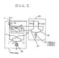
- Fig. 5 shows a fifth embodiment of this invention which is similar to the embodiment of Fig. 1 except that a differential amplifier 20 is added.
- the differential amplifier 20 serves as a buffer for the oscillator.
- the differential amplifier 20 includes a pair of NPN transistors 21 and 22.
- the collectors of the transistors 21 and 22 are connected to the positive power supply terminal 7 via resistors 21A and 22A respectively.
- the base of the transistor 21 is connected to the junction 14 between the collector of the transistor 1 and the resonator 4 within the oscillator.
- the base of the transistor 22 is connected to the junction 11 between the collector of the transistor 2 and the resonator 4 within the oscillator. In this way, the buffer amplifier 20 is directly coupled to the oscillator without using any coupling capacitor.
- the emitters of the transistors 21 and 22 are connected in common, and are grounded via a constant current circuit 23.
- the buffer amplifier 20 dispenses with any bypass capacitor or grounding capacitor. It should be noted that the resistor 10 may be replaced by a diode as in the embodiment of Fig. 2.
- a pair of RF signals are generated at the collectors of the transistors 21 and 22 respectively in accordance with the oscillation signal. These RF signals have opposite phases. In general, at least one of the RF signals is outputted to an external circuit.
- Fig. 6 shows a sixth embodiment of this invention.
- the embodiment of Fig. 6 includes an oscillating section 100 identical with any one of the oscillators of Figs. 1-4.
- the embodiment of Fig. 6 includes a cascade combination of buffer amplifiers 40 and 60, and a cascade combination of buffer amplifiers 50 and 70.
- the buffer amplifiers 40, 50, 60, and 70 have similar internal designs. Specifically, each of the buffer amplifiers 40, 50, 60, and includes a differential amplifier of a single-phase drive type.
- the cascade combination of the buffer amplifiers 40 and 60 is connected between the oscillating section 100 and an external circuit.
- the oscillation signal is transmitted to the external circuit via the buffer amplifiers 40 and 60.
- the cascade combination of the buffer amplifiers 50 and 70 is connected between the oscillating section 100 and a prescaler. The oscillation signal is transmitted to the prescaler via the buffer amplifiers 50 and 70.
- the buffer amplifier 40 includes a pair of NPN transistors 44 and 45.
- the collectors of the transistors 44 and 45 are connected to the positive power supply terminal 7 via resistors 42 and 43 respectively.
- the base of the transistor 44 is directly coupled to an output terminal of the oscillating section 100 which corresponds to the junction 11 or 14 (see Figs. 1-4).
- the base of the transistor 45 is connected to the output terminal of the oscillating section 100 via a resistor 47.
- the emitters of the transistors 44 and 45 are connected in common, and are grounded via a constant current circuit 46.
- the base of the transistor 45 is grounded via a bypass capacitor 48.
- the bypass capacitor 48 shunts an RF signal to the ground which returns from the collector to the base of the transistor 45, so that a good isolation between an input side and an output side of the buffer amplifier 40 is ensured with respect to the RF signal.
- the buffer amplifier 60 includes a pair of NPN transistors 64 and 65. The collectors of the transistors
- the 64 and 65 are connected to the positive power supply terminal 7 via resistors 62 and 63 respectively.
- the base of the transistor 64 is directly connected to the collector of the transistor 45 within the buffer amplifier 40.
- the base of the transistor 65 is connected to the collector of the transistor 45 within the buffer amplifier 40 via a resistor 67.
- the emitters of the transistors 64 and 65 are connected in common, and are grounded via a constant current circuit 66.
- the base of the transistor 65 is grounded via a bypass capacitor 68.
- the operation and effect of the bypass capacitor 68 are similar to those of the bypass capacitor 48 of the buffer amplifier 40.
- An RF signal is generated at the collector of the transistor 65 in accordance with the oscillation signal. The RF signal is outputted from the collector of the transistor 65 to the external circuit.
- the buffer amplifier 50 includes a pair of NPN transistors 54 and 55.
- the collectors of the transistors 54 and 55 are connected to the positive power supply terminal 7 via resistors 52 and 53 respectively.
- the base of the transistor 54 is directly coupled to the output terminal of the oscillating section 100.
- the base of the transistor 55 is connected to the output terminal the oscillating section 100 via a resistor 57.
- the emitters of the transistors 54 and 55 are connected in common, and are grounded via a constant current circuit 56.
- the base of the transistor 55 is grounded via a bypass capacitor 58.
- the operation and effect of the bypass capacitor 58 are similar to those of the bypass capacitor 48 of the buffer amplifier 40.
- the buffer amplifier 70 includes a pair of NPN transistors 74 and 75.
- the collectors of the transistors 74 and 75 are connected to the positive power supply terminal 7 via resistors 72 and 73 respectively.
- the base of the transistor 74 is directly connected to the collector of the transistor 55 within the buffer amplifier 50.
- the base of the transistor 75 is connected to the collector of the transistor 55 within the buffer amplifier 50 via a resistor 77.
- the emitters of the transistors 74 and 75 are connected in common, and are grounded via a constant current circuit 76.
- the base of the transistor 75 is grounded via a bypass capacitor 78.
- the operation and effect of the bypass capacitor 78 are similar to those of the bypass capacitor 48 of the buffer amplifier 40.
- a pair of RF signals are generated at the collectors of the transistors 74 and 75 respectively in accordance with the oscillation signal. These RF signals have opposite phases. The RF signals are outputted from the collectors of the transistors 74 and 75 to the prescaler.
- An oscillator includes first and second transistors and a parallel resonant circuit.
- the resonant circuit has first and second ends. The first end of the resonant circuit is connected to a base of the first transistor and a collector of the second transistor. The second end of the resonant circuit is connected to base of the second transistor and a collector of the first transistor.
- a voltage dropping device is connected between the first end of the resonant circuit and a power supply for providing a voltage drop to expose the first and second transistors to driving voltages lower than a voltage of the power supply.
Landscapes
- Inductance-Capacitance Distribution Constants And Capacitance-Resistance Oscillators (AREA)
Applications Claiming Priority (4)
| Application Number | Priority Date | Filing Date | Title |
|---|---|---|---|
| JP158673/89 | 1989-06-21 | ||
| JP1158673A JPH0324806A (ja) | 1989-06-21 | 1989-06-21 | 発振器 |
| JP25403/90 | 1990-02-05 | ||
| JP2025403A JP2621536B2 (ja) | 1990-02-05 | 1990-02-05 | 発振器 |
Publications (3)
| Publication Number | Publication Date |
|---|---|
| EP0404080A2 true EP0404080A2 (de) | 1990-12-27 |
| EP0404080A3 EP0404080A3 (de) | 1991-04-17 |
| EP0404080B1 EP0404080B1 (de) | 1996-04-24 |
Family
ID=26362995
Family Applications (1)
| Application Number | Title | Priority Date | Filing Date |
|---|---|---|---|
| EP90111596A Expired - Lifetime EP0404080B1 (de) | 1989-06-21 | 1990-06-19 | Schaltung zur Speisung einer externen Schaltung und eines Vorteilers mit einem Oszillatorsignal |
Country Status (3)
| Country | Link |
|---|---|
| US (1) | US5055804A (de) |
| EP (1) | EP0404080B1 (de) |
| DE (1) | DE69026649T2 (de) |
Cited By (2)
| Publication number | Priority date | Publication date | Assignee | Title |
|---|---|---|---|---|
| GB2284953A (en) * | 1993-12-14 | 1995-06-21 | Samsung Electronics Co Ltd | Oscillator for synchronous video detector using anti-resonant circuit in differential amplifier inputs and feedback |
| EP0689283A1 (de) * | 1994-06-24 | 1995-12-27 | Plessey Semiconductors Limited | Abstimmbarer Oszillator |
Family Cites Families (12)
| Publication number | Priority date | Publication date | Assignee | Title |
|---|---|---|---|---|
| JPS4966056A (de) * | 1972-10-27 | 1974-06-26 | ||
| US3963996A (en) * | 1974-09-05 | 1976-06-15 | Zenith Radio Corporation | Oscillation system for integrated circuit |
| JPS5274263A (en) * | 1975-12-17 | 1977-06-22 | Sony Corp | Oscillation circuit |
| US4063193A (en) * | 1976-10-12 | 1977-12-13 | National Semiconductor Corporation | Differential transistor pair integrated circuit oscillator with L-C tank circuit |
| US4243953A (en) * | 1979-02-16 | 1981-01-06 | Rca Corporation | Voltage controlled oscillator presenting high impedance to parallel resonant tank circuit |
| US4270102A (en) * | 1979-04-26 | 1981-05-26 | General Electric Company | Integrated circuit FM local oscillator with AFC control and temperature compensation |
| US4346351A (en) * | 1980-02-28 | 1982-08-24 | National Semiconductor Corporation | High frequency voltage-controlled oscillator |
| US4353039A (en) * | 1980-05-15 | 1982-10-05 | Gte Automatic Electric Laboratories, Inc. | Monolithic astable multivibrator circuit |
| JPS57133705A (en) * | 1981-02-12 | 1982-08-18 | Toshiba Corp | Variable frequency oscillating circuit |
| JPS5814604A (ja) * | 1981-07-20 | 1983-01-27 | Sanyo Electric Co Ltd | Am変調回路 |
| US4633195A (en) * | 1985-11-21 | 1986-12-30 | Motorola, Inc. | Balanced oscillator with constant emitter voltage level |
| JP2521963B2 (ja) * | 1987-07-01 | 1996-08-07 | ソニー株式会社 | 発振回路 |
-
1990
- 1990-06-08 US US07/534,866 patent/US5055804A/en not_active Expired - Lifetime
- 1990-06-19 EP EP90111596A patent/EP0404080B1/de not_active Expired - Lifetime
- 1990-06-19 DE DE69026649T patent/DE69026649T2/de not_active Expired - Lifetime
Cited By (3)
| Publication number | Priority date | Publication date | Assignee | Title |
|---|---|---|---|---|
| GB2284953A (en) * | 1993-12-14 | 1995-06-21 | Samsung Electronics Co Ltd | Oscillator for synchronous video detector using anti-resonant circuit in differential amplifier inputs and feedback |
| GB2284953B (en) * | 1993-12-14 | 1998-06-24 | Samsung Electronics Co Ltd | Controlled oscillator as for synchronous video detector |
| EP0689283A1 (de) * | 1994-06-24 | 1995-12-27 | Plessey Semiconductors Limited | Abstimmbarer Oszillator |
Also Published As
| Publication number | Publication date |
|---|---|
| DE69026649T2 (de) | 1996-09-26 |
| EP0404080B1 (de) | 1996-04-24 |
| US5055804A (en) | 1991-10-08 |
| EP0404080A3 (de) | 1991-04-17 |
| DE69026649D1 (de) | 1996-05-30 |
Similar Documents
| Publication | Publication Date | Title |
|---|---|---|
| US5513389A (en) | Push pull buffer with noise cancelling symmetry | |
| US4536662A (en) | Bidirectional constant current driving circuit | |
| EP0893878B1 (de) | Hochfrequenz-Oszillatorschaltung | |
| US5418500A (en) | High-frequency oscillator circuit | |
| US5717363A (en) | Oscillation circuit and oscillation method | |
| US4660002A (en) | High frequency oscillator using a diode for frequency switching and FM modulation | |
| US6163222A (en) | Buffer amplifier with frequency selective mechanism | |
| US4194158A (en) | Integrated front end circuit for VHF receiver | |
| US5055804A (en) | Oscillator | |
| EP0760554A1 (de) | Direktmischende, ein unsymmetrisches Signal empfangende und eine Ausgangsspannung mit minimierter Offsetspannung am Ausgang liefernde Frequenzmischschaltung | |
| US6542042B1 (en) | Low power crystal oscillator with feedback resistor pair | |
| EP0140430B1 (de) | Schaltungsanordnung zur Frequenzvervielfachung | |
| US6836190B2 (en) | Oscillator device and electronic apparatus using the same | |
| US4633195A (en) | Balanced oscillator with constant emitter voltage level | |
| EP0232560A1 (de) | Verstärker-Mischerschaltung für UHF | |
| JP2004023570A (ja) | 平衡型発振器およびそれを用いた電子装置 | |
| US5584069A (en) | HF mixing stage in the form of a common-base circuit | |
| US6388517B1 (en) | Input change-over type amplifier and frequency change-over type oscillator using the same | |
| EP0821470A1 (de) | Spannungsgesteuerte Oszillatorschaltung | |
| US6522211B1 (en) | Frequency-switching oscillator and communication apparatus using same | |
| JPH0974321A (ja) | 送受信機 | |
| US4303890A (en) | Circuit arrangement for transferring a signal | |
| US7205856B2 (en) | Piezoelectric oscillator | |
| JPH09162641A (ja) | 電圧制御発振器 | |
| SU1633501A1 (ru) | Входное устройство радиоприемника |
Legal Events
| Date | Code | Title | Description |
|---|---|---|---|
| PUAI | Public reference made under article 153(3) epc to a published international application that has entered the european phase |
Free format text: ORIGINAL CODE: 0009012 |
|
| 17P | Request for examination filed |
Effective date: 19900619 |
|
| AK | Designated contracting states |
Kind code of ref document: A2 Designated state(s): DE FR GB |
|
| PUAL | Search report despatched |
Free format text: ORIGINAL CODE: 0009013 |
|
| AK | Designated contracting states |
Kind code of ref document: A3 Designated state(s): DE FR GB |
|
| 17Q | First examination report despatched |
Effective date: 19931214 |
|
| RAP1 | Party data changed (applicant data changed or rights of an application transferred) |
Owner name: MATSUSHITA ELECTRIC INDUSTRIAL CO., LTD. |
|
| GRAA | (expected) grant |
Free format text: ORIGINAL CODE: 0009210 |
|
| AK | Designated contracting states |
Kind code of ref document: B1 Designated state(s): DE FR GB |
|
| REF | Corresponds to: |
Ref document number: 69026649 Country of ref document: DE Date of ref document: 19960530 |
|
| ET | Fr: translation filed | ||
| PLBE | No opposition filed within time limit |
Free format text: ORIGINAL CODE: 0009261 |
|
| STAA | Information on the status of an ep patent application or granted ep patent |
Free format text: STATUS: NO OPPOSITION FILED WITHIN TIME LIMIT |
|
| 26N | No opposition filed | ||
| REG | Reference to a national code |
Ref country code: GB Ref legal event code: IF02 |
|
| PGFP | Annual fee paid to national office [announced via postgrant information from national office to epo] |
Ref country code: DE Payment date: 20090615 Year of fee payment: 20 Ref country code: GB Payment date: 20090617 Year of fee payment: 20 |
|
| REG | Reference to a national code |
Ref country code: GB Ref legal event code: PE20 Expiry date: 20100618 |
|
| PG25 | Lapsed in a contracting state [announced via postgrant information from national office to epo] |
Ref country code: GB Free format text: LAPSE BECAUSE OF EXPIRATION OF PROTECTION Effective date: 20100618 |
|
| PG25 | Lapsed in a contracting state [announced via postgrant information from national office to epo] |
Ref country code: DE Free format text: LAPSE BECAUSE OF EXPIRATION OF PROTECTION Effective date: 20100619 |
|
| PGFP | Annual fee paid to national office [announced via postgrant information from national office to epo] |
Ref country code: FR Payment date: 20090611 Year of fee payment: 20 |