EP0404225A2 - Funkempfänger - Google Patents
Funkempfänger Download PDFInfo
- Publication number
- EP0404225A2 EP0404225A2 EP90201518A EP90201518A EP0404225A2 EP 0404225 A2 EP0404225 A2 EP 0404225A2 EP 90201518 A EP90201518 A EP 90201518A EP 90201518 A EP90201518 A EP 90201518A EP 0404225 A2 EP0404225 A2 EP 0404225A2
- Authority
- EP
- European Patent Office
- Prior art keywords
- filter
- resonators
- filter section
- adjacent
- radio receiver
- Prior art date
- Legal status (The legal status is an assumption and is not a legal conclusion. Google has not performed a legal analysis and makes no representation as to the accuracy of the status listed.)
- Withdrawn
Links
Images

Classifications
-
- H—ELECTRICITY
- H03—ELECTRONIC CIRCUITRY
- H03H—IMPEDANCE NETWORKS, e.g. RESONANT CIRCUITS; RESONATORS
- H03H7/00—Multiple-port networks comprising only passive electrical elements as network components
- H03H7/01—Frequency selective two-port networks
- H03H7/09—Filters comprising mutual inductance
-
- H—ELECTRICITY
- H04—ELECTRIC COMMUNICATION TECHNIQUE
- H04B—TRANSMISSION
- H04B1/00—Details of transmission systems, not covered by a single one of groups H04B3/00 - H04B13/00; Details of transmission systems not characterised by the medium used for transmission
- H04B1/06—Receivers
- H04B1/16—Circuits
- H04B1/1638—Special circuits to enhance selectivity of receivers not otherwise provided for
Definitions
- the present invention relates to a radio receiver having a front end filter comprising helical resonators.
- filters having helical resonators in radio frequency applications represents a well known technology. These devices can be used in the 10 MHz to 1.5 GHz region with typical Q's from 200 to 5000. Currently such devices are being used as high Q bandpass filters, band rejection filters, reference cavities, tuning elements for oscillators, front end filters for receivers, and for many other applications where high Q is paramount and large size prohibitive.
- a conventional helical filter consists of a number of helical resonators enclosed in a rectangular or circular shield, each consisting of a quarter-wavelength transmission line wound in the form of a single layer helix on a circular former, the helical transmission lines being wound in the same direction, short-circuited at the same end (to the shield) and open circuited at the other.
- the resonators are coupled to each other via openings in partitions between them, the size and location of the openings affecting the coupling coefficient between the resonators and thereby the frequency response of the filter.
- a disadvantage of using conventional helical resonators in the front end filter of a radio receiver is that in order to obtain satisfactory image frequency rejection many conventional helical resonators are needed, involving significant costs.
- a further disadvantage of using conventional helical resonators is that the amount of coupling is controlled by the size and location of the openings in the partitions which must be accurately machined, again involving significant costs.
- the invention comprises a radio receiver comprising a filter having one or more filter sections, each filter section comprising a shield having therein a plurality of helical resonators each having a quarter-wavelength transmission line wound in the form of a helix with the transmission lines adjacent resonators being wound in opposite directions and being grounded at opposite ends, whereby the frequency response of the filter section has a transmission notch on the high frequency side of the filter section passband, and one or more grounded shielding pins being disposed between adjacent helical resonators at such locations whereby the transmission notch in the frequency response of the filter section is steered to be coincident with or near to the image frequency.
- the present invention is based on the recognition that by using such a filter section as distinct from one using conventional helical resonators a transmission notch is generated on the high frequency side of the passband and that by steering the transmission notch in the frequency response to be coincident with or near to the image frequency, extra image frequency rejection is gained. As a consequence a reduced number of helical resonators may be utilised to obtain the required image frequency rejection than if conventional helical resonators were used. Moreover the use of shielding pins avoids the costs that are associated with the use of partitions in conventional helical resonators.
- the filter comprises two said filter sections, the output of one being coupled to the input of the other, and each filter section having two said helical resonators.
- This receiver which is suitable for operation in the VHF band, uses a limited number of helical resonators as compared with a conventional receiver.
- each of the filter sections comprises one shielding pin which is disposed between said adjacent helical resonators at a central location. It has been found that by using a central shielding pin the receiver is suitable for operation over the band (146 MHz - 174 MHz), with the central location of the shielding pin steering the transmission notch near to the image frequency.
- each of the filter section comprises two shieldings pins which are disposed between said adjacent helical resonators, the shielding pins being located at opposite ends of the adjacent resonators. It has been found that this filter is suitable for operation over the band (68 MHz - 88 MHz), with the configuration of the shielding pins steering the transmission notch near to the image frequency.
- the output of one filter section is coupled to the input of another filter section via an amplifier.
- This embodiment has the advantage that the S/N ratio of the output signal of the first filter section does not significantly deteriorate beyond the amplifier.
- each of the helical resonators is coupled to a varicap diode network whereby the filter can be electronically tuned.
- This embodiment provides a receiver with a wide tuning range end ensures good image rejection over the passband.
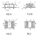
- the filter section 1 shown in Figures 1A, 1B, 1C has its application in a VHF radio receiver front-end for operation over the band (146 - 174 MHz), the radio receiver front-end being illustrated in Figure 3.
- the filter section 1 consists of two helical resonators 2, 3 coupled to each other via an opening 4, each helical resonator being a quarter-wave length section of a shielding helical transmission line 8, grounded at one end 6 and open circuited at the other end 7.
- the helices 8 are formed by winding 24 gauge wire of enamelled copper on respective horizontal cylindrical formers 9a, 9b of low-loss thermoplastic. Each helix has 10 turns and is evenly distributed over the former in a single layer.
- a shielding pin 14 which is made of tin copper wire having a diameter of 1 mm is disposed between the helical resonators 2, 3 at a central position and is secured to a shield cover 10 and grounded to the circuit board 13. This shielding pin 14 is used to control the coupling between the resonators 2, 3 and in turn the frequency response of the filter section 1.
- the filter section may comprise more than two helical resonators, wherein adjacent helical resonators have opposite winding directions, are grounded at opposing ends and have shielding pins located between them.
- each former 9a, 9b of the filter section 1 has a diameter of 5.5 mm and length of 10 mm, and is disposed with in the shield cover 10 so that its longitudinal axis is 5 mm from both the top and side wall of the shield with the longitudinal axes of the formers being 13 mm apart.
- the shield cover 10 is made of brass and is of a rectangular cross section of dimensions 10 mm x 17 mm x 23 mm with open ends 11, 12 and is attached and grounded to the circuit board 13. Experiments have shown that this shield cover does not adversely effect filter performance and there appears to be very little fringing field exterior to the shield cover and no detuning effects are apparent when operated in the presence of a overall housing.
- the initial fine tuning and alignment is achieved with copper or aluminium slugs (not shown) inserted into the high voltage ends of the coils, namely the open circuited ends.
- input and output coupling to the filter section is provided by taps, not shown, to the appropriate impedance points on the helical transmission lines.
- the input and output coupling to the filter section may be provided by means of a probe or a loop in known manner.
- a "helical interdigital" coil structure which has been derived in part from the microwave stripline counterpart and the more conventional helical resonators.
- This "helical interdigital" coil structure is shown in figure 1C.
- the winding directions of these adjacent helices 8 are opposite, being clockwise on former 9a and anticlockwise on former 9b, and the helices 8 being grounded at ends 6 which oppose each other.
- the frequency response of the filter section 1 is shown in Figure 4.
- This filter section has been electronically tuned to a centre frequency 31 of 174 MHz by a varicap diode network and has a transmission notch 32 at 203 MHz on the high frequency side of the centre frequency.
- This transmission notch is generated due to the nature of the coupling mechanism between the resonators 2,3 of the filter section 1, the helices winding direction and their orientation with respect to ground.
- the current magnitude in the loaded helical resonators reach a maximum at the grounded end 6 and the voltage reach a maximum at the open circuited end 7 which in the "interdigital helical" coil structure are opposing one another.
- the locating of the grounded shielded pin at the centre between the helical resonators will decrease the transmission notch frequency, which appears to be the result of the mutual coupling being reduced by virtue of the shorted turn effect reflecting an increased inductance into each helical winding, which in turn raises the equivalent coupling inductance and lowers the transmission notch frequency.
- one or more shielded pins 14 may be located between the helices at the ends of the resonators which raises the transmission notch frequency, which appears to be the result of the pins tending to increase the electric flux to ground and reducing the mutually coupled capacitance and thereby raising the transmission notch frequency.
- the pin diameter has a significant effect on coupling between the helices and a second order effect on the notch position wherein there is an optimal pin diameter for each band, however a pin diameter of 1 mm is suitable for all bands.
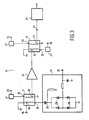
- FIG 3 shows a circuit diagram of a front end filter 15 for a radio receiver.
- the front end filter consists of two filter sections 16, 17 both of the same type as shown in Figures 1A, 1B, 1C.
- the RF signal is fed to input 18 of the front end filter 15 which is coupled to the tap 19 of the filter section 16, the output signal of filter section 16 is supplied by tap 20, and is fed to an RF amplifier 21 so that the S/N ratio of the signal does not significantly deteriorate beyond the amplifier, and this signal is fed to the tap 22 of filter section 17, the output signal of filter section 17 being supplied by tap 23 and fed to the output 24 of the front end filter 15 which is coupled to the mixer 25.
- the front end filter may comprise one filter section and a RF amplifier coupled thereto, the output of the filter being taken from the output of the RF amplifier.
- the frequency response of the filter 15 when tuned to a centre frequency 31 of 174 MHz is illustrated in Figure 5.
- the full rejection of the image frequency 33 of 217 MHz cannot be resolved without overloading the RF amplifier but is in principle greater than 85 dB over the full band (146-174 MHz).
- a front end filter using conventional helical resonators would require more resonators than the present filter in order to obtain image rejection specifications of 85 dB.
- Each open circuited end 26 of the helices in the filter 15 is end loaded with a varicap diode network 27 which is used to electronically tune the filter 15 over the band (146-174 MHz) with a 1 db nose bandwidth of 4 MHz.
- the electronic tuning of the resonators is provided by the varicap diodes which are biased by an appropriate voltage supplied on a voltage source input 30.
- the capacitance end loading of the helices will lower the unloaded resonant frequency of the filter sections and is used to down tune the filter sections 16, 17 to the desired frequency in the band (146-174 MHz).
- Experiments have confirmed that the location of the transmission notch tracks closely to the passband when electronically tuned ensuring good image rejection over the tuning bandwidth.
- the unloaded resonant frequency of the filter sections 16, 17 may be chosen to be 2.4 to 2.8 times that of the top frequency in the band (146-174 MHz) which represents a good compromise between tuning range and insertion loss and the number of turns is then determined from the helical filter design equations of Zverev.
- fu unloaded resonator frequency
- f1 loaded resonator frequency
- Zo resonantor characteristic impedance.
- the varicap diode network 27 is used to minimize intermodulation distortion and four varicap diodes 28 are used to limit the insertion loss of the filter section to less than 2.5dB with a typical 1dB nose bandwidth of 5MHz.
- the value of capacitance of the capacitor 29 and varicap diodes 28 in series with the open circuited end 26 of the helix is set in conjunction with the varicap tuning range and the number of turns of the helix to cover the desired band. Fine tuning is achieved with copper or aluminium tuning slugs.
- the tap point on each helix is chosen to be at 3/4 of a turn for the band (146-174MHz). This was chosen to be compatible with the type of horizontal formers 9a,9b used and any mismatch in impedance may be accounted for by a capacitor divider network in known manner (not shown).
- the insertion loss of a filter of this type increases when the open circuited end 26 of the resonator is taken to a circuit board pad connection. This is due to losses within the circuit board itself and is reduced in this application by relieving the ground plane area underneath the end connection of the helix.
- FIG. 2 A further embodiment of a filter section which is suitable for operation over the band (68-88MHz) is shown in figure 2. It has been found that the transmission notch associated with a single central pin has dropped too low to be effective in image rejection in this band. In this embodiment the transmission notch is raised by using two edge pins in lieu of one central pin, a common shield cover 10 is used with provision for both pin locations.
Landscapes
- Engineering & Computer Science (AREA)
- Computer Networks & Wireless Communication (AREA)
- Signal Processing (AREA)
- Control Of Motors That Do Not Use Commutators (AREA)
- Input Circuits Of Receivers And Coupling Of Receivers And Audio Equipment (AREA)
Applications Claiming Priority (2)
| Application Number | Priority Date | Filing Date | Title |
|---|---|---|---|
| AUPJ481289 | 1989-06-19 | ||
| AU4812/89 | 1989-06-19 |
Publications (2)
| Publication Number | Publication Date |
|---|---|
| EP0404225A2 true EP0404225A2 (de) | 1990-12-27 |
| EP0404225A3 EP0404225A3 (de) | 1992-07-01 |
Family
ID=3774001
Family Applications (1)
| Application Number | Title | Priority Date | Filing Date |
|---|---|---|---|
| EP19900201518 Withdrawn EP0404225A3 (de) | 1989-06-19 | 1990-06-13 | Funkempfänger |
Country Status (5)
| Country | Link |
|---|---|
| US (1) | US5036302A (de) |
| EP (1) | EP0404225A3 (de) |
| JP (1) | JPH0334702A (de) |
| CA (1) | CA2019073A1 (de) |
| FI (1) | FI903018A7 (de) |
Families Citing this family (6)
| Publication number | Priority date | Publication date | Assignee | Title |
|---|---|---|---|---|
| US7064749B1 (en) | 1992-11-09 | 2006-06-20 | Adc Technology Inc. | Portable communicator |
| JP4736212B2 (ja) * | 2001-03-14 | 2011-07-27 | 井関農機株式会社 | 畝立成形装置 |
| JP3684506B2 (ja) | 2002-03-22 | 2005-08-17 | 株式会社東京機械製作所 | 縦ミシン目形成装置 |
| JP2005244456A (ja) * | 2004-02-25 | 2005-09-08 | Sharp Corp | 回路装置 |
| US8471664B1 (en) * | 2012-04-24 | 2013-06-25 | Zippy Technology Corp. | Transformer without coil racks |
| CN109712777B (zh) * | 2019-02-26 | 2023-11-24 | 中国科学院上海微系统与信息技术研究所 | 滤波器、测试系统及滤波器的制备方法 |
Family Cites Families (7)
| Publication number | Priority date | Publication date | Assignee | Title |
|---|---|---|---|---|
| US3939443A (en) * | 1972-01-07 | 1976-02-17 | Finommechanikai Vallalat | Frequency-selective coupling for high-frequency electromagnetic waves |
| GB1602770A (en) * | 1977-06-03 | 1981-11-18 | Matsushita Electric Industrial Co Ltd | Band pass filter |
| CA1128152A (en) * | 1978-05-13 | 1982-07-20 | Takuro Sato | High frequency filter |
| JPS58182501U (ja) * | 1982-05-27 | 1983-12-05 | アルプス電気株式会社 | 中間周波帯域炉波器 |
| JPS60140901A (ja) * | 1983-12-27 | 1985-07-25 | Matsushita Electric Ind Co Ltd | ヘリカルフイルタ |
| US4662001A (en) * | 1985-08-15 | 1987-04-28 | Zenith Electronics Corporation | Tunable notch filter for image frequency and conducted local oscillator leakage rejection |
| JPS6292602A (ja) * | 1985-10-18 | 1987-04-28 | Fujitsu Ltd | ヘリカルフイルタ |
-
1990
- 1990-06-13 EP EP19900201518 patent/EP0404225A3/de not_active Withdrawn
- 1990-06-15 CA CA002019073A patent/CA2019073A1/en not_active Abandoned
- 1990-06-15 FI FI903018A patent/FI903018A7/fi not_active Application Discontinuation
- 1990-06-15 US US07/539,094 patent/US5036302A/en not_active Expired - Fee Related
- 1990-06-15 JP JP2157421A patent/JPH0334702A/ja active Pending
Also Published As
| Publication number | Publication date |
|---|---|
| FI903018A7 (fi) | 1990-12-20 |
| FI903018A0 (fi) | 1990-06-15 |
| US5036302A (en) | 1991-07-30 |
| JPH0334702A (ja) | 1991-02-14 |
| CA2019073A1 (en) | 1990-12-19 |
| EP0404225A3 (de) | 1992-07-01 |
Similar Documents
| Publication | Publication Date | Title |
|---|---|---|
| JP3238167B2 (ja) | チューニング可能なバンドパス・フィルタ | |
| US5023866A (en) | Duplexer filter having harmonic rejection to control flyback | |
| US4431977A (en) | Ceramic bandpass filter | |
| DE68913574T2 (de) | An der Oberfläche angebrachtes Filter mit integralem Übertragungsleitunsanschluss. | |
| US4963843A (en) | Stripline filter with combline resonators | |
| KR920010600B1 (ko) | 대역저지 기능을 갖춘 필터 및 송수절환기 | |
| US5717368A (en) | Varactor tuned helical resonator for use with duplex filter | |
| US4074214A (en) | Microwave filter | |
| US6686815B1 (en) | Microwave filter | |
| US6215374B1 (en) | Magnetically coupled resonators for achieving low cost narrow band pass filters having high selectivity, low insertion loss and improved out-of-band rejection | |
| US5594395A (en) | Diode tuned resonator filter | |
| US5515015A (en) | Transceiver duplex filter utilizing saw filter | |
| US4456895A (en) | Band selectable tunable bandpass filter | |
| GB2165098A (en) | Radio frequency filters | |
| KR900008522B1 (ko) | 송신선 장치 | |
| JP3344428B2 (ja) | 誘電体共振器および誘電体共振部品 | |
| CA2089155C (en) | Multi-stage monolithic ceramic bandstop filter with isolated filter stages | |
| US3936776A (en) | Interspersed double winding helical resonator with connections to cavity | |
| DE10202699B4 (de) | Nichtreziprokes Schaltungsbauelement und Kommunikationsvorrichtung, die dasselbe enthält | |
| US5406234A (en) | Tunable microwave filter apparatus having a notch resonator | |
| US4247837A (en) | Multi-conductor ferromagnetic resonant coupling structure | |
| US5036302A (en) | Radio receiver filter with image rejection | |
| US4586007A (en) | Notch filter | |
| KR102686326B1 (ko) | 세라믹 유전체를 이용하여 소형화 및 고출력이 가능한 대역저지필터 | |
| US4313097A (en) | Image frequency reflection mode filter for use in a high-frequency receiver |
Legal Events
| Date | Code | Title | Description |
|---|---|---|---|
| PUAI | Public reference made under article 153(3) epc to a published international application that has entered the european phase |
Free format text: ORIGINAL CODE: 0009012 |
|
| AK | Designated contracting states |
Kind code of ref document: A2 Designated state(s): DE FR GB IT SE |
|
| PUAL | Search report despatched |
Free format text: ORIGINAL CODE: 0009013 |
|
| AK | Designated contracting states |
Kind code of ref document: A3 Designated state(s): DE FR GB IT SE |
|
| 17P | Request for examination filed |
Effective date: 19921221 |
|
| 17Q | First examination report despatched |
Effective date: 19941012 |
|
| STAA | Information on the status of an ep patent application or granted ep patent |
Free format text: STATUS: THE APPLICATION IS DEEMED TO BE WITHDRAWN |
|
| 18D | Application deemed to be withdrawn |
Effective date: 19950606 |