EP0405424A2 - Gerät zur Herstellung eines elektrostatischen latenten Bildes - Google Patents
Gerät zur Herstellung eines elektrostatischen latenten Bildes Download PDFInfo
- Publication number
- EP0405424A2 EP0405424A2 EP90112085A EP90112085A EP0405424A2 EP 0405424 A2 EP0405424 A2 EP 0405424A2 EP 90112085 A EP90112085 A EP 90112085A EP 90112085 A EP90112085 A EP 90112085A EP 0405424 A2 EP0405424 A2 EP 0405424A2
- Authority
- EP
- European Patent Office
- Prior art keywords
- styluses
- control electrodes
- latent image
- recording medium
- electrostatic
- Prior art date
- Legal status (The legal status is an assumption and is not a legal conclusion. Google has not performed a legal analysis and makes no representation as to the accuracy of the status listed.)
- Granted
Links
Images


Classifications
-
- B—PERFORMING OPERATIONS; TRANSPORTING
- B41—PRINTING; LINING MACHINES; TYPEWRITERS; STAMPS
- B41J—TYPEWRITERS; SELECTIVE PRINTING MECHANISMS, i.e. MECHANISMS PRINTING OTHERWISE THAN FROM A FORME; CORRECTION OF TYPOGRAPHICAL ERRORS
- B41J2/00—Typewriters or selective printing mechanisms characterised by the printing or marking process for which they are designed
- B41J2/385—Typewriters or selective printing mechanisms characterised by the printing or marking process for which they are designed characterised by selective supply of electric current or selective application of magnetism to a printing or impression-transfer material
- B41J2/39—Typewriters or selective printing mechanisms characterised by the printing or marking process for which they are designed characterised by selective supply of electric current or selective application of magnetism to a printing or impression-transfer material using multi-stylus heads
-
- G—PHYSICS
- G03—PHOTOGRAPHY; CINEMATOGRAPHY; ANALOGOUS TECHNIQUES USING WAVES OTHER THAN OPTICAL WAVES; ELECTROGRAPHY; HOLOGRAPHY
- G03G—ELECTROGRAPHY; ELECTROPHOTOGRAPHY; MAGNETOGRAPHY
- G03G15/00—Apparatus for electrographic processes using a charge pattern
- G03G15/22—Apparatus for electrographic processes using a charge pattern involving the combination of more than one step according to groups G03G13/02 - G03G13/20
- G03G15/32—Apparatus for electrographic processes using a charge pattern involving the combination of more than one step according to groups G03G13/02 - G03G13/20 in which the charge pattern is formed dotwise, e.g. by a thermal head
- G03G15/321—Apparatus for electrographic processes using a charge pattern involving the combination of more than one step according to groups G03G13/02 - G03G13/20 in which the charge pattern is formed dotwise, e.g. by a thermal head by charge transfer onto the recording material in accordance with the image
- G03G15/325—Apparatus for electrographic processes using a charge pattern involving the combination of more than one step according to groups G03G13/02 - G03G13/20 in which the charge pattern is formed dotwise, e.g. by a thermal head by charge transfer onto the recording material in accordance with the image using a stylus or a multi-styli array
Definitions
- the present invention relates to an electrostatic latent image forming apparatus of the uniplane control type which is capable of forming, by applying voltage pulses of opposite polarities to styluses and control electrodes which are arranged closely to one-another in one plane, an electrostatic latent image on an electrostatic latent image recording medium formed by a dielectric layer or by a combination of a dielectric layer and at least one conductive layer, which medium is in contact with the styluses and the control electrodes.
- Figure 6 is a schematic sectional view of a conventional example of such uniplane control type electrostatic latent image forming apparatus
- Figure 7 is an electric equivalent circuit diagram thereof.
- reference numeral 11 denotes an electrostatic recording paper as an electrostatic latent image recording medium, which is formed by four layers including a surface electrostatic layer 1, an intermediate conductive layer 2, a paper base 3 and a back resistance layer (conductive layer) 4.
- Reference numeral 8 denotes a stylus
- numerals 7a and 7b denote control electrodes.
- Reference numeral 9 denotes a stylus drive circuit for applying to the stylus 8 a recording voltage pulse having a negative polarity
- numeral 10 denotes a control electrode drive circuit for applying to the control electrodes 7a and 7b a recording voltage pulse having a positive polarity.
- Reference numeral 6 denotes a pad roller used for pressing the electrostatic recording paper 11 against the stylus 8 and the control electrodes 7a and 7b, which pad roller is made of an insulating material (such as polyurethane foam).
- the stylus drive circuit 9 acts to apply a recording voltage pulse of a negative polarity to the stylus 8 and, at the same time, the control electrode drive circuit 10 acts to apply a recording voltage pulse of a positive polarity to the control electrodes 7a and 7b.
- the difference in potential between the stylus 8 and the dielectric layer 1 at the position directly below the stylus 8 exceeds a predetermined value, so that discharge is caused to take place between the stylus 8 and the dielectric layer 1. Then, negative charge is transferred from the stylus 8 to the dielectric layer 1 and stored in the latter, thereby forming an electrostatic latent image on the electrostatic recording paper 11.
- Each of the layers of the electrostatic recording paper 11 has the following function or service.
- the surface dielectric layer 1 is made of a mixture of insulating thermoplastic resin and insulating pigment so that it serves as a charge carrier for holding charged particles for a long time and it serves to form a discharge gap of about 10 ⁇ m between the stylus 8 and the control electrodes 7a and 7b with the aid of an insulating pigment having a diameter of about 3 to 6 ⁇ m.
- Function of the intermediate conductive layer 2 is to effectively concentrate the positive voltage applied to the control electrodes 7a and 7b in the dielectric layer 1 at a position thereof located directly below the stylus 8.
- This layer also serves as a liquid barrier so that, in coating the dielectric layer 1 on the paper base 3, the resin and the pigment are prevented from immersing into cavities in the paper base 3 to assure the coating with a uniform thickness.
- the paper base 3 serves as a part for constituting a base on which the intermediate layer 2 and the dielectric layer 1 are formed and, at the same time, it usually contains water existing in equilibrium with the ambient humidity so as to perform the same function as the intermediate conductive layer 2.
- the back resistance layer 4 does not directly take part in the formation of the electrostatic latent image like the intermediate layer 2, except that it serves to raise the potential at a position directly below the stylus 8, but it contributes to prevention of any fog caused by the bias due to the rise in potentials of the intermediate layer 2 and the paper base 3 in forming the electrostatic latent image.
- the intermediate conductive layer and the back resistance layer of the electrostatic recording paper are made of an electronic conductive material so as to be hardly affected by the humidity (water content).
- this gives rise to another problem that the cost of the electrostatic recording paper is increased.
- an object of the present invention is to provide a uniplane control type electrostatic latent image forming apparatus which is capable of forming stably an electrostatic latent image without being affected by the humidity even with use of the same electrostatic recording paper as a conventional one.
- a conductive member is provided to be brought into pressure contact with a portion of an electrostatic latent image recording medium at the back surface thereof which portion is opposed to styluses and control electrodes.
- the resistance of the conductive member is connected in parallel to the resistance of the electrostatic latent image recording medium itself so that apparent resistance value of the electrostatic latent image recording medium in areas between the stylus and the control electrodes is reduced and less varies due to humidity, with the result that the potential at a position directly below the stylus can rise sufficiently even at high or low humidity, thereby making it possible to stably form a electrostatic latent image.
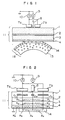
- Figure 1 is a schematic sectional view of a uniplane control type electrostatic latent image forming apparatus according to a first embodiment of the present invention
- Figure 2 is an electric equivalent circuit diagram thereof.
- the same reference numerals as those in Figures 6 and 7 are used to denote the same or corresponding parts so that explanation thereof will be omitted.
- reference numeral 12 denotes a pad roller used for pressing an electrostatic recording paper 11 against a stylus 8 and control electrodes 7a and 7b, which pad roller is formed by bonding on the surface of a roller member 13 made of an insulating material such as polyurethane foam a conductive rubber member 14 having a surface resistivity of about 105 ⁇ to 107 ⁇ as a conductive member introduced by the present invention.
- the conductive rubber member 14 is brought into pressure contact at constant pressure with a portion of the back surface of the electrostatic recording paper 11, which portion is opposed to the stylus 8 and the control electrodes 7a and 7b, as shown in Figure 1. Further, the conductive rubber member 14 is kept from coming in direct contact with other conductive members.
- the surface resistivity of the conductive rubber member 14 can be measured by means of, for example, "High Resistance Meter 4329A” and “Resistivity Cell 16008A” which are manufactured by YOKOGAWA Hewlett-Packard Co., Ltd.
- the stylus drive circuit 9 and the control electrode drive circuit 10 act to apply simultaneously a recording voltage pulse of a negative polarity and a recording voltage pulse of a positive polarity respectively to the stylus 8 and the control electrodes 7a and 7b which are opposed to the electrostatic recording paper 11 with a proper discharge gap kept therebetween.
- the recording voltage pulse of a positive polarity applied to the control electrodes 7a and 7b raises electric potentials of the intermediate conductive layer 2, the paper base 3, the back resistance layer 4 and the conductive rubber member 14 at positions thereof located directly below the control electrodes 7a and 7b placed in capacitive coupling by an electrostatic capacitance Cc possessed by the dielectric layer 1.
- This rise in the potential is transferred to a position of each layer directly below the stylus 8 by resistivities Rc, Rp, Rb and Rs of the intermediate conductive layer 2, the paper base 3, the back resistance layer 4 and the conductive rubber member 14, respectively, and then appears on the surface of the dielectric layer 1 at a position directly below the stylus 8 through an electrostatic capacitance Cp.
- the resistance value between points directly below the stylus 8 and the control electrode 7a, 7b is determined mainly by the smallest resistance value among the above four resistivities. Namely, if the surface resistivity Rs of the conductive rubber member 14 is set at a value smaller than Rc, Rp and Rb, the resistance value between the points directly below the stylus 8 and the control electrodes 7a, 7b is mainly dominated by Rs and prevented from exceeding the value of Rs (Rc and Rb at normal temperature and humidity are generally set at about 107 ⁇ ).
- Rc is set at a proper value smaller than Rc, Rp and Rb, it is possible to maintain the condition that discharge takes place stably between the stylus 8 and the electrostatic recording paper 11 because, even at high or low humidity which causes Rc, Rp and Rb to decrease or increase, a change in the resistance value between the points directly below the stylus 8 and the control electrodes 7a, 7b can be minimized. It is therefore possible to stably form an electrostatic latent image without being affected by the ambient humidity.
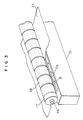
- FIG 3 is a schematic perspective view of a more practical uniplane control type electrostatic latent image forming apparatus according to a second embodiment of the present invention.
- reference numeral 15 denotes a multistylus electrostatic recording head, in which styluses 8 are arranged in a line at constant intervals in its face opposite to the electrostatic recording paper 11 with the control electrodes 7a and 7b (7b being not shown) arranged in two lines in a manner to interpose the styluses 8 therebetween.
- Figure 4 illustrates the detailed structure of the multistylus electrostatic recording head 14.
- the styluses 8 belonging to the A-channel blocks are connected correspondingly to A-channel stylus drive circuits 9a in number m through common signal lines, while the styluses 8 belonging to the B-channel blocks are connected correspondingly to B-channel stylus drive circuits 9b in number m through common signal lines.
- control electrodes 7a, 7b each have a width substantially equal to the width of arrangement of the styluses 8 of one block and are disposed to interpose therebetween half the styluses 8 of two adjacent blocks as shown in the drawing.
- Each pair of control electrodes 7a and 7b are connected to the associated control electrode drive circuit 10 through a common signal line.
- the electrodes are driven in the following manner.
- the A-channel stylus drive circuits 9a are activated to apply recording voltage pulse of a negative polarity to the styluses 8 belonging to the A-channel blocks and, at the same time, the control electrode drive circuits 10 are activated to apply recording voltage pulse of a positive polarity to two pairs of control electrodes 7a and 7b between which the styluses 8 of a first A-channel block (Block No. A-1 shown in Figure 4) are interposed, thus forming a part of the electrostatic latent image directly below the styluses 8 of Block No. A-1.
- the B-channel stylus drive circuits 9b are activated to apply the recording voltage pulse to the styluses 8 belonging to the B-channel blocks and, at the same time, the recording voltage pulse is applied to two pairs of control electrodes 7a and 7b between which the styluses 8 of Block No. B-1 are interposed, thus forming another part of the electrostatic latent image directly below the styluses 8 of Block No. B-1.
- the electrostatic latent image part for each block is formed alternately by the A-channel blocks and the B-channel blocks.
- reference numeral 16 denotes a pad roller used for pressing the electrostatic recording paper 11 against the styluses 8 and the control electrodes 7a and 7b, which pad roller is formed by attaching separate conductive members 18 on the surface of a roller member 17 made of an insulating material (such as polyurethane foam).
- a roller member 17 made of an insulating material (such as polyurethane foam).
- Each of the separate conductive members 18 is made of a material which has a surface resistivity of about 0 ⁇ and is regarded as a perfect conductor.
- the conductive members 18 are electrically insulated from one another. Further, it goes without saying that the respective conductive members 18 are prevented from coming in direct contact with other conductive members.
- Each of the separate conductive members 18 has a width substantially equal to the width of the control electrodes 7a, 7b and is located in a manner to be brought into pressure contact with the back surface of the electrostatic recording paper 11 only in an area opposed to an appointed pair of control electrodes 7a and 7b and the styluses 8 interposed between them.
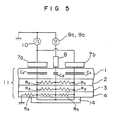
- the electric equivalent circuit of the apparatus of this embodiment can be expressed as shown in Figure 5, because the conductive member 18 is almost a perfect conductor. Namely, the resistance value between the points directly below the stylus 8 and the control electrodes 7a, 7b is nearly zero and the potentials of the dielectric layer 1 at the positions directly below the stylus 8 and the control electrodes 7a, 7b are substantially equal to each other.
- the electrostatic latent image forming process adopted in this embodiment is the same as that in the aforesaid first embodiment.
- the conductive member 18 is brought into pressure contact to raise the potential at the position directly below the stylus 8 up to a potential substantially equal to the potential at the position directly below the control electrodes 7a, 7b and therefore, it is possible to allow discharge to take place efficiently between the stylus 8 and the dielectric layer 1.
- This condition is unchanged even if Rc, Rp and Rb of the electrostatic recording paper 11 are varied in accordance with the change in the ambient humidity. In consequence, it is possible to stably form an electrostatic latent image even at low or high humidity.
- the conductive members 18 are separate, the potentials of only the conductive members 18 corresponding to two pairs of control electrodes to which the positive polarity recording voltage pulse is applied, are raised without substantially raising the potentials of other conductive members 18. Accordingly, there is no possibility of occurrence of the ghost image due to expansion of the potential into the unnecessary portion.
- the potential of the whole conductive member 18 is raised to allow the ghost image to occur. It is not permissible, therefore, to use a perfect conductor as a material for the conductive member 18, and it is required to use a material having a certain surface resistivity, such as conductive rubber.
- these resistance values may be set at rather high level.
- the conductive member is mounted on the pad roller so as to be rotated together with electrostatic recording paper, it may be formed as an elastic sheet member, for example.
- the coefficient of friction thereof with the electrostatic recording paper should be reduced so as not to apply load to the electrostatic recording paper during conveyance.
- the separate conductive members can also be made of a material having a certain surface resistivity, such as conductive rubber.
- the electrostatic latent image recording medium is not limited to one described in connection with the above embodiments.
- the thickness of the conductive layer which causes increase in cost of the electrostatic latent image recording medium can be made thin (resulting in the increase of the resistance value thereof), thereby making it possible as well to reduce the cost of the electrostatic latent image recording medium.
Landscapes
- Physics & Mathematics (AREA)
- General Physics & Mathematics (AREA)
- Printers Or Recording Devices Using Electromagnetic And Radiation Means (AREA)
- Dot-Matrix Printers And Others (AREA)
- Electrophotography Using Other Than Carlson'S Method (AREA)
Applications Claiming Priority (2)
| Application Number | Priority Date | Filing Date | Title |
|---|---|---|---|
| JP1165934A JPH0329965A (ja) | 1989-06-28 | 1989-06-28 | 静電潜像形成装置 |
| JP165934/89 | 1989-06-28 |
Publications (3)
| Publication Number | Publication Date |
|---|---|
| EP0405424A2 true EP0405424A2 (de) | 1991-01-02 |
| EP0405424A3 EP0405424A3 (en) | 1991-04-24 |
| EP0405424B1 EP0405424B1 (de) | 1994-03-23 |
Family
ID=15821794
Family Applications (1)
| Application Number | Title | Priority Date | Filing Date |
|---|---|---|---|
| EP90112085A Expired - Lifetime EP0405424B1 (de) | 1989-06-28 | 1990-06-26 | Gerät zur Herstellung eines elektrostatischen latenten Bildes |
Country Status (4)
| Country | Link |
|---|---|
| US (1) | US5150133A (de) |
| EP (1) | EP0405424B1 (de) |
| JP (1) | JPH0329965A (de) |
| DE (1) | DE69007551T2 (de) |
Cited By (1)
| Publication number | Priority date | Publication date | Assignee | Title |
|---|---|---|---|---|
| WO1997030380A1 (en) * | 1996-02-15 | 1997-08-21 | Minnesota Mining And Manufacturing Company | Method and apparatus to reduce fogging in electrostatic printing |
Families Citing this family (2)
| Publication number | Priority date | Publication date | Assignee | Title |
|---|---|---|---|---|
| DE4205304A1 (de) * | 1992-02-21 | 1993-08-26 | Heidelberger Druckmasch Ag | Schaltungsanordnung fuer einen reversiblen bildaufbau einer druckform einer druckmaschine |
| US6137519A (en) * | 1997-06-12 | 2000-10-24 | 3M Innovative Properties Company | System and method for reducing striations in electrostatic printing |
Family Cites Families (8)
| Publication number | Priority date | Publication date | Assignee | Title |
|---|---|---|---|---|
| US3626422A (en) * | 1969-07-28 | 1971-12-07 | Varian Associates | Electrographic-writing head having a preponderance of conductive portions engaging the recording medium |
| US4366491A (en) * | 1978-11-21 | 1982-12-28 | Masaru Ohnishi | Electrographic imaging system |
| JPS57124752A (en) * | 1981-01-27 | 1982-08-03 | Fuji Xerox Co Ltd | Forming method for electrostatic recording picture image |
| JPS57138959A (en) * | 1981-02-23 | 1982-08-27 | Fuji Xerox Co Ltd | Holding mechanism of electrostatic recording head |
| JPS5814774A (ja) * | 1981-07-20 | 1983-01-27 | Ricoh Co Ltd | 静電記録方法および装置 |
| JPS58107375A (ja) * | 1981-12-21 | 1983-06-27 | Minolta Camera Co Ltd | 静電記録装置 |
| JPH0614670B2 (ja) * | 1983-09-26 | 1994-02-23 | 株式会社リコー | 静電記録装置 |
| FR2589273B1 (fr) * | 1985-10-28 | 1987-12-11 | Telephonie Ind Commerciale | Tete d'impression electrostatique d'image |
-
1989
- 1989-06-28 JP JP1165934A patent/JPH0329965A/ja active Pending
-
1990
- 1990-06-20 US US07/540,942 patent/US5150133A/en not_active Expired - Fee Related
- 1990-06-26 EP EP90112085A patent/EP0405424B1/de not_active Expired - Lifetime
- 1990-06-26 DE DE69007551T patent/DE69007551T2/de not_active Expired - Fee Related
Cited By (2)
| Publication number | Priority date | Publication date | Assignee | Title |
|---|---|---|---|---|
| WO1997030380A1 (en) * | 1996-02-15 | 1997-08-21 | Minnesota Mining And Manufacturing Company | Method and apparatus to reduce fogging in electrostatic printing |
| US5815188A (en) * | 1996-02-15 | 1998-09-29 | Minnesota Mining And Manufacturing Co. | Method and apparatus to reduce fogging in electrostatic printing |
Also Published As
| Publication number | Publication date |
|---|---|
| EP0405424B1 (de) | 1994-03-23 |
| DE69007551T2 (de) | 1994-09-01 |
| EP0405424A3 (en) | 1991-04-24 |
| US5150133A (en) | 1992-09-22 |
| JPH0329965A (ja) | 1991-02-07 |
| DE69007551D1 (de) | 1994-04-28 |
Similar Documents
| Publication | Publication Date | Title |
|---|---|---|
| US3611419A (en) | Electrographic imaging system and heads therefor | |
| CA1140982A (en) | Electrographic stylus writing apparatus | |
| US4920343A (en) | Capacitive keyswitch membrane with self contained sense-to-ground capacitance | |
| EP0567019B1 (de) | Plasmaadressierte elektrooptische Vorrichtung | |
| US3626422A (en) | Electrographic-writing head having a preponderance of conductive portions engaging the recording medium | |
| US5359395A (en) | Contact charge supply device | |
| US4030107A (en) | Electrographic recording devices employing electrostatic induction electrodes | |
| US3792495A (en) | Electrostatic recorder employing three voltage level switching between the stylus electrodes and the backplate sections | |
| US5150133A (en) | Electrostatic latent image forming apparatus | |
| US6515692B2 (en) | Image forming apparatus having writing electrodes as a writing device | |
| GB1580391A (en) | Electrographic writing system | |
| US4438444A (en) | Multi-stylus head | |
| US4607269A (en) | Electrostatic print head | |
| US4476473A (en) | Electrostatic record image forming method | |
| US4719481A (en) | Electrographic ion writing head driver system | |
| US3596284A (en) | Electrographic apparatus employing plural inkers of different colors for separating signal levels or channels according to color | |
| US6160567A (en) | Electrostatic write head for electronic printing press | |
| US3217330A (en) | Electrostatic printing utilizing printthrough recording | |
| US3235874A (en) | Electrostatic printer utilizing an array of mutually insulated pin electrodes | |
| US4366491A (en) | Electrographic imaging system | |
| EP0013160B1 (de) | Verfahren und Vorrichtung zur Bestimmung der Spannung, bei der in der Elektrographie ein Paschen-Durchbruch auftritt | |
| US4811158A (en) | Solid state charger | |
| GB1559641A (en) | Electrographic printing head | |
| JPH0343991B2 (de) | ||
| JPS5848060A (ja) | 静電記録体および静電記録方法 |
Legal Events
| Date | Code | Title | Description |
|---|---|---|---|
| PUAI | Public reference made under article 153(3) epc to a published international application that has entered the european phase |
Free format text: ORIGINAL CODE: 0009012 |
|
| AK | Designated contracting states |
Kind code of ref document: A2 Designated state(s): DE FR GB |
|
| 17P | Request for examination filed |
Effective date: 19901228 |
|
| PUAL | Search report despatched |
Free format text: ORIGINAL CODE: 0009013 |
|
| AK | Designated contracting states |
Kind code of ref document: A3 Designated state(s): DE FR GB |
|
| 17Q | First examination report despatched |
Effective date: 19920929 |
|
| GRAA | (expected) grant |
Free format text: ORIGINAL CODE: 0009210 |
|
| AK | Designated contracting states |
Kind code of ref document: B1 Designated state(s): DE FR GB |
|
| REF | Corresponds to: |
Ref document number: 69007551 Country of ref document: DE Date of ref document: 19940428 |
|
| ET | Fr: translation filed | ||
| PLBE | No opposition filed within time limit |
Free format text: ORIGINAL CODE: 0009261 |
|
| STAA | Information on the status of an ep patent application or granted ep patent |
Free format text: STATUS: NO OPPOSITION FILED WITHIN TIME LIMIT |
|
| 26N | No opposition filed | ||
| PGFP | Annual fee paid to national office [announced via postgrant information from national office to epo] |
Ref country code: FR Payment date: 19970610 Year of fee payment: 8 |
|
| PGFP | Annual fee paid to national office [announced via postgrant information from national office to epo] |
Ref country code: GB Payment date: 19970617 Year of fee payment: 8 |
|
| PGFP | Annual fee paid to national office [announced via postgrant information from national office to epo] |
Ref country code: DE Payment date: 19970704 Year of fee payment: 8 |
|
| PG25 | Lapsed in a contracting state [announced via postgrant information from national office to epo] |
Ref country code: GB Free format text: LAPSE BECAUSE OF NON-PAYMENT OF DUE FEES Effective date: 19980626 |
|
| GBPC | Gb: european patent ceased through non-payment of renewal fee |
Effective date: 19980626 |
|
| PG25 | Lapsed in a contracting state [announced via postgrant information from national office to epo] |
Ref country code: FR Free format text: LAPSE BECAUSE OF NON-PAYMENT OF DUE FEES Effective date: 19990226 |
|
| PG25 | Lapsed in a contracting state [announced via postgrant information from national office to epo] |
Ref country code: DE Free format text: LAPSE BECAUSE OF NON-PAYMENT OF DUE FEES Effective date: 19990401 |
|
| REG | Reference to a national code |
Ref country code: FR Ref legal event code: ST |