EP0405530A2 - Dispositif de commutation de cellules - Google Patents
Dispositif de commutation de cellules Download PDFInfo
- Publication number
- EP0405530A2 EP0405530A2 EP90112305A EP90112305A EP0405530A2 EP 0405530 A2 EP0405530 A2 EP 0405530A2 EP 90112305 A EP90112305 A EP 90112305A EP 90112305 A EP90112305 A EP 90112305A EP 0405530 A2 EP0405530 A2 EP 0405530A2
- Authority
- EP
- European Patent Office
- Prior art keywords
- cell
- cells
- output
- stage
- input
- Prior art date
- Legal status (The legal status is an assumption and is not a legal conclusion. Google has not performed a legal analysis and makes no representation as to the accuracy of the status listed.)
- Granted
Links
Images


Classifications
-
- H—ELECTRICITY
- H04—ELECTRIC COMMUNICATION TECHNIQUE
- H04L—TRANSMISSION OF DIGITAL INFORMATION, e.g. TELEGRAPHIC COMMUNICATION
- H04L12/00—Data switching networks
- H04L12/54—Store-and-forward switching systems
- H04L12/56—Packet switching systems
- H04L12/5601—Transfer mode dependent, e.g. ATM
-
- H—ELECTRICITY
- H04—ELECTRIC COMMUNICATION TECHNIQUE
- H04L—TRANSMISSION OF DIGITAL INFORMATION, e.g. TELEGRAPHIC COMMUNICATION
- H04L49/00—Packet switching elements
- H04L49/25—Routing or path finding in a switch fabric
- H04L49/253—Routing or path finding in a switch fabric using establishment or release of connections between ports
- H04L49/255—Control mechanisms for ATM switching fabrics
-
- H—ELECTRICITY
- H04—ELECTRIC COMMUNICATION TECHNIQUE
- H04L—TRANSMISSION OF DIGITAL INFORMATION, e.g. TELEGRAPHIC COMMUNICATION
- H04L12/00—Data switching networks
- H04L12/54—Store-and-forward switching systems
- H04L12/56—Packet switching systems
- H04L12/5601—Transfer mode dependent, e.g. ATM
- H04L2012/5672—Multiplexing, e.g. coding, scrambling
Definitions
- the present invention relates to a cell exchange apparatus for high-speed exchange of various information such as sound, data and picture information in the form of blocks which are called cells.
- a switching network which is called Banyan-network, has heretofore been known as one example of the system in which data is divided into cells and the header information of each cell is directly referred to by hardware means to thereby perform high-speed switching.
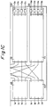
- Fig. 7 is a block diagram of a conventional cell exchange apparatus which is disclosed, for example in IEEE Journal on Selected Areas in Communications Vol. SAC-4, No. 8, November 1986, pp. 1373 - 1380.
- reference numerals 1a and 1b denote cells each comprising a header section and a data section, 2 input ports to which cells 1 (1 denoting generally the cells 1a and 1b) are inputted, 3 a cell exchange apparatus that performs switching of cells 1 which are inputted to input ports 2, 4 2x2 unit switches serving as space switches which constitute the cell exchange apparatus 3, and 5 output ports of the cell exchange apparatus 3.
- each of the unit switches 4 that are arrayed in the first row from the left as viewed in Fig. 7 performs a switching operation such that, if the top bit in the header section of a cell 1 is "0", the unit switch 4 connects the input port thereof to the upper output port thereof, whereas, if the top bit is "1", it connects the input port to the lower output port.
- the unit switches 4 that are arrayed in the second row from the left similarly perform a switching operation in accordance with the state of the second bit in the header section of the cell 1. If such unit switches 4 are interconnected as shown in Fig. 7 and the number of a desired output port 5 in the final stage is expressed as a binary number and put to the header section of a cell 1, the cell 1 arrives at the desired output port 5 no matter from which input port 2 it is inputted.
- the conventional cell exchange apparatus having the above-described arrangement suffers, however, from the following problems. If cells 1a and 1b which are directed to the same output port 5 are simultaneously inputted to input ports 2, blocking (collision) occurs. In order to solve this problem, a system wherein a buffer memory is provided in the input section or inside of each unit switch 4 has been proposed. With this prior art system, however, the buffer memory is likely to be blocked when cells 1 which are directed to one output port 5 are concentrated therein.
- a cell exchange apparatus comprising: an input-stage cell exchange switch module having an input-stage cell multiplexing means which subjects input cells to time-division multiplexing for each of a plurality of groups each comprising a plurality of input ports through which cells are inputted, and an input-stage cell selecting means which selects, from an output signal from the input-stage cell multiplexing means, a cell that is directed to a specific one of a plurality of groups each comprising a plurality of output ports and outputs the selected cell; at least one output-stage cell exchange switch module having memory means each of which stores a cell that is outputted from a cell selecting means in the pre-stage to a specific output port group, a memory control means which controls and stores the addresses of cells stored in each memory means according to the destination and reads out cells from the memory means according to a predetermined output rule, an output-stage cell multiplexing means which multiplexes cells that are outputted from the memory means, and an output-
- cells which arrive at all input ports are divided into a plurality of groups and once multiplexed by the input-stage cell multiplexing means that is provided in an input-stage cell exchange switch module for each group before being distributed to respective output ports through address filters that comprise the cell selecting means.
- At least one output-stage cell exchange switch module that receives the output of the input-stage cell exchange switch module writes the cells into the memory means and effects multiplexing of cells again by the cell multiplexing means for each of a plurality of groups of output ports under the control of the memory control means. Thereafter, the multiplexed cells are each distributed to the desired output port through a final address filter that comprises the cell selecting means. Thus, the probability of cells being wasted is lowered.
- each individual buffer memory in the above-described cell exchange apparatus is adapted to be common to all the incoming lines to make uniform the amount of cells being held in each buffer memory, thereby preventing the occurrence of blocking and even more effectively reducing the effect of the concentration of cells in one output port on other output ports.
- the cell exchange apparatus is further provided with a space switch that effects spatial switching with respect to each of the cells which are outputted from the cell selecting means in the input-stage cell exchange switch module, and cells which are outputted from the space switch are written into memory means.
- the memory control means controls and stores the addresses of cells stored in the memory means, according to the destination, and monitors the amount of cells being held in the memory means and reads out cells preferentially from one which is directed to a destination for which a relatively large amount of cells is being held in the memory means.
- the output-stage cell exchange switch module can preferentially store cells into memory means which have a relatively small amount of cells being held therein and can also read cells preferentially from one which is directed to a destination for which a relatively large amount of cells is being held in the memory means. It is therefore possible to make uniform the amount of cells being held in each memory means (buffer memory). Thus, the probability of cells being wasted is lowered, and even if cells are concentrated in one output port, the cell exchange apparatus is capable of switching without affecting cells which are directed to other output ports.
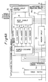
- Fig. 1 is a circuit diagram showing the general arrangement of a cell exchange apparatus 3 according to a first embodiment of the present invention.
- the cell exchange apparatus 3 has input-stage cell exchange switch modules 60 to 63 which are provided to correspond to respective groups of cell input ports 2 to exchange cells which are inputted to the corresponding groups of input ports 2, output-stage cell exchange switch modules 70 to 73 which exchange cells that are delivered from cell exchange switch modules in the pre-stage to specific output port groups, and cell output-stage modules 80 to 83 which constitute final-stage modules.
- the module 60 for example, has an input-stage cell multiplexing circuit 7 which subjects cells to time-division multiplexing, and input-stage cell selecting circuits 8a to 8d each of which selects and outputs through an address filter a cell which is directed to a specific one of the groups of output ports.
- the output-stage cell exchange switch modules 70 to 73 for example, the switch module 70, which is shown in Fig.
- header processing circuits 9a to 9d each of which reads and analyzes the destination information of a cell that is outputted from the corresponding cell selecting circuit in the pre-stage to a specific output port group and then outputs the cell; memory circuits 10a to 10d in which when write addresses are designated, cells that are outputted from the header processing circuits 9a to 9d are stored at the designated addresses, and when read addresses are designated, the stored cells are read out irrespective of the order in which they were written; an address exchange circuit 16 which is provided in a memory control circuit 11 to distribute the addresses of cells that are written in the memory circuits 10a to 10d into output port groups (hereinafter referred to as "outgoing lines") while referring to the header processing circuits 9a to 9d; outgoing line corresponding address FIFO memories 17a to 17d which enables distributed addresses to be written therein in correspondence to outgoing lines and in the order of arrival; a read enable circuit 18 which gives a read address to each of the memory circuits 10
- Fig. 5 exemplarily shows the operation of the input-stage cell exchange switch module 60.
- Cells in input signals A to D are subjected to time-division multiplexing in the cell multiplexing circuit 7 to form a signal E that is shown in Fig. 5.
- the signal E is delivered to the input-stage cell selecting circuits 8a to 8d which respectively correspond to the output ports of the inputstage cell exchange switch module 60, in which the first addresses that are put to the header sections of cells are detected to select and output cells which are to be delivered to given output ports, as exemplarily shown by signals F and P.
- FIG. 5 shows the way in which a cell, the first address of which is "1”, is outputted as a signal F, while a cell, the first address of which is "2", is outputted as a signal P.
- multiplexing is effected at a rate which is determined by multiplying the link rate of input ports by the number of ports, for example, with synchronized time slots each corresponding to one cell, as shown in Fig. 5.
- a time slot which contains no input cell is defined as a vacant slot, which is assigned a first address that corresponds to none of the output ports.
- Fig. 2 exemplarily shows the module 70.
- the signals F to I comprise cells which are delivered to the signals lines in a burst matter at the speed of multiplexing and therefore vary in the number of cells. Accordingly, these signals are supplied to the memory circuits 10a to 10d for buffering, which are provided to correspond to the input ports in the output-stage cell exchange switch module 70.
- the outputs of the memory circuits 10a to 10d are multiplexed in the output-stage cell multiplexing circuit 12. It is considered that if input cells arrive uniformly both temporally and spatially, all cells which are inputted to the output-stage cell exchange switch module 70 can be multiplexed without being wasted on condition that the rate of the output signal J from the output-stage cell multiplexing circuit 12 is not lower than a rate which is determined by multiplying the input link rate of the output-stage cell exchange switch module 70 by the number of ports. In actual practice, however, the arrival of cells varies both temporally and spatially and it is therefore necessary to buffer cells in the memory circuits 10a to 10d to thereby absorb overflow of cells.
- the memory control circuit 11 has a function to prevent successively reading cells which are addressed to the same outgoing line and also prevent inversion of the order in which cells are read out. More specifically, when cells are stored in the memory circuits 10a to 10d, the addresses of the cells in the memory circuits 10a to 10d are distributed into outgoing lines by the address exchange circuit 16 and these addresses are then stored in the outgoing line corresponding address FIFO memories 17a to 17d in order to control and store the addresses of the cells in the memory circuits 10a to 10d in correspondence to the outgoing lines.
- the read enable circuit 18 refers to the outputs of the FIFO memories 17a to 17d and gives read addresses to all the memory circuits 10a to 10d to send out cells therefrom within the range in which the output-stage (post-stage) cell multiplexing circuit 12 is capable of multiplexing the outputs of all the memory circuits 10a to 10d.
- a variety of methods may be considered usable to control reading from the memory circuits 10a to 10d, for example, a method wherein N (an integer not less than 2) cells are read out in successivesion with respect to an outgoing line for which the amount of cells being held in the FIFO memories 17a to 17d is greater than a predetermined value, while n (1 or 0) cell is read out with respect to other outgoing lines, thereby effecting multiplexing; and a method wherein the amounts of cells which are addressed to various outgoing lines are compared with each other, and N cells are read out in succession with respect to an outgoing line for which the amount of cells being held is the largest, while n cell is read out with respect to other outgoing lines, for multiplexing purpose.
- an output-stage cell exchange switch module 70 as one example, which is not one in the final stage but in an intermediate stage that is followed by another output-stage cell exchange switch module.
- the description will be made with reference to the timing charts of Figs. 5 and 6, in regard to a multiplexing method wherein two cells are read out in succession with respect to an outgoing line for which the number of cells being held exceeds 4 (equivalent to the number of input ports), while 1 or 0 cell is read out with respect to an outgoing line for which said number is not greater than 4.
- the signal G shows that a series of nine cells is delivered from the input-stage cell exchange switch module 61 to outgoing lines K, L, M and N.
- the FIFO memories 17a, 17b, 17c and 17d correspond to the outgoing lines K, L, M and N, respectively.
- the read enable circuit 18 monitors the amount of cells being held in each of the FIFO memories 17a to 17d. First, at the time when the address at which a first cell is stored is stored in any of the FIFO memories 17a to 17d, the read gate of the FIFO memory 17a corresponding to the outgoing line K is opened to fetch an address.
- the first cell is a first cell in the signal F, which is directed to the outgoing line K (each cell being hereinafter denoted by a number, e.g., Fl, that is put to the data section of the cell).
- an address is first fetched from the FIFO memory 17a and this address is given as a read address to the memory circuit 10a to read out and multiplex the corresponding cell.
- the read address is supplied to the vacant address control circuit 191a.
- an address is fetched from the FIFO memory 17b corresponding to the outgoing line L to multiplex the cell G2.
- an address would otherwise be fetched from the FIFO memory 17c corresponding to the outgoing line M, but the FIFO memory 17c is vacant and consequently the process immediately shifts to the FIFO memory 17d corresponding to the outgoing line N.
- an address is fetched therefrom, and the cell G3 is multiplexed.
- the cell Gl that is addressed to the outgoing line K is multiplexed, followed by the cell I1 to the outgoing line L, the cell G6 to the outgoing line M, and the cell G7 to the outgoing line N.
- the process then proceeds to the FIFO memory 17a corresponding to the outgoing line K. Since the number of cells being held in the FIFO memory 17a at this time is 5 (indicated by O in Fig. 4), two addresses are successively read out therefrom. Thus, the cells H1 and G4 are multiplexed. Thereafter, the cells H2, H3, G5, G9, F3, H5, F2, H4, I2, G8, F4 and G10 are multiplxed in the mentioned order.
- the FIFO memories 17a to 17b in the output-stage cell exchange switch module 70 it is possible to control the addresses in the memory circuits 10a to 10d and cells can be temporarily stored therein.
- the sum total of cells which are supplied to the output-stage cell exchange switch modules 70 to 73 from the signal lines corresponds, on the average, to a rate which is determined by multiplying the input link rate by the number of input ports as long as there is neither temporal nor spatial deviation, and it is therefore considered to be equal to or less than the total number of cells which can be multiplexed on multiplex signals that are produced in the output-stage cell exchange switch modules 70 to 73.
- the memory circuits 10a to 10d in the output-stage cell exchange switch modules 70 to 73 are capable of writing at a high rate of multiplexing and also capable of reading at the link rate of the outgoing lines even if a plurality of cells arrive simultaneously. Accordingly, even if a plurality of cells are concentrated at the same time, no cell is wasted as long as the number of cells concentrated is within the capacity of the memory circuits 10a to 10d.
- the respective numbers of input and output ports in the whole cell exchange switch are the same, the numbers of input and output ports may be different from each other.
- the number of stages of the output-stage cell exchange switch modules 70 to 73 may also be increased as desired.
- the numbers of input and output ports in the whole cell exchange switch are each 16 and each cell exchange switch module has 4 input ports and 4 output ports, these numbers may be changed as desired.
- the cell exchange apparatus of the present invention is not necessarily divided into modules such as those described above but may be fabricated in the form of a single cell exchange switch.
- the number of an outgoing line is put to the header section of a cell for each of the two address sections for two groups of cell exchange switch modules which are provided in two stages.
- the number of an outgoing line may be represented by another form, for example, a coded number which is put to a single address section of a cell.
- the arrangement may also be such that the header and data sections of cells are separated from each other and these sections are assigned to a plurality of signal lines, which are arranged in parallel, by use of respective circuits which have different rates of transmission.
- the link rate of the input ports is the same as the output port rate, if the rate of reading from the output-stage memory circuits 10a to 10d, shown in Fig. 1, is made higher than the input port link rate, traffic concentration can be achieved, and it is also possible to make the input port link rate higher than the output port rate.
- the multiplexing rate of the signal J is the same as that of the signal E, if the multiplexing rate of the signal J is made higher, it is possible to further reduce the rate at which cells are wasted in transmission between cell exchange switch module stages.
- the FIFO memories 17a to 17d are provided to correspond to the outgoing lines, respectively, of the output-stage cell exchange switch module 70, it is also possible to provide a plurality of FIFO memories for each outgoing line according to the order of priority so that a cell of higher priority" is first multiplexed on the basis of a sign representative of a level of priority that is added to the header section of a cell in addition to an address.
- the read enable circuit 18 is arranged such that when the number of cells being held in any one of the FIFO memories 17a to 17d exceeds 4, two cells are successively read out therefrom, it should be noted that the number is not necessarily limitative to 4 and that any other numerical value may be employed.
- the present invention may be applied to any system wherein reading from an FIFO memory which has a relatively large number of cells being held therein is preferentially executed.
- a serial-to-parallel converter circuit and a parallel-to-serial converter circuit may be added to the input and output ends, respectively, of this switch to process data in the form of parallel signals.
- the cell exchange apparatus is arranged such that input cells are multiplexed in an input-stage cell exchange switch module before being distributed, and in an output-stage cell exchange switch module a cell string which is inputted from a pre-stage cell exchange switch module is stored in memory circuits and the cells in the memory circuits are read out according to a predetermined output rule by a memory control circuit. Accordingly, even if cells are concentrated in a specific output port group at the same time, no cell is wasted as long as the number of cells concentrated is within the capacity of the output-stage memory circuits.
- FIG. 3 the same reference numerals as those shown in Fig. 1 denote the same elements, and in Fig. 4, the same reference numerals as those shown in Fig. 2 denote the same elements.
- the second embodiment is the same as the first embodiment in regard to the arrangements of many portions; therefore, description of the same portions is omitted to prevent complication.
- reference numeral 4 denotes space switches that operate in such a manner that cells, which are outputted from the input-stage cell selecting circuits in the input-stage cell exchange switch modules 60 to 63 to specific output port groups, are preferentially stored in memory means (memory circuits; described later) 10a to 10d (10e to 10h) which have a relatively small amount of cells being held therein, in order to make uniform the amount of cells being held among the memory circuits 10a to 10d (10e to 10h).
- memory means memory circuits; described later
- reference numeral 15 that is shown in the memory control circuit 11 denotes a memory circuit counter which controls the amount of cells being held in each of the memory circuits 10a to 10d.
- the space switch 4 refers to the counter 15 for the amount of cells being held in each of the memory circuits 10a to 10d and stores each input cell preferentially in a memory circuit which has a relatively small amount of cells being held therein, thereby making the amount of cells being held as uniform as possible among the memory circuits 10a to 10d.
- the space switch 4 refers to the memory circuit counter 15 in the memory control circuit 11 and, when m cells arrive at the same time, the space switch 4 selects from among the memory circuits 10a to 10d m memory circuits, from one which has the smallest amount of cells being held therein, and successively writes the cells in the selected memory circuits, respectively.
- the cells that are outputted from the space switch 4 are delivered to given memory circuits 10a to 10d through the corresponding header processing circuits 9a to 9d, which analyze the destinations of the cells concerned and deliver the identification information of the corresponding ones of outgoing lines K to N to the address exchange circuit 16 in the memory control circuit 11.
- the addresses where the cells are stored are delivered to the address exchange circuit 16 by the corresponding vacant address control circuits 19a to 19d.
- the address exchange circuit 16 stores the delivered addresses in the FIFO memories 17a to 17d corresponding to the outgoing lines K to N which are designated by the header processing circuits 9a to 9d.
- the memory circuit counter 15 counts and controls the amount of cells being held in each of the memory circuits 10a to 10d.
- the above-described second embodiment provides the following advantages: Since the space switch 4 is employed to preferentially write cells in memory circuits 10a to 10d (10e to 10h) which have a relatively small amount of cells being held therein in order to make the amount of cells being held as uniform as possible among the memory circuits 10a to 10d (10e to 10h), the memory circuits 10a to 10d (10e to 10h) can perform in substantially the same way as in the case of a single relatively large memory circuit which is mutually used for all the incoming lines. It is therefore possible to further reduce the rate at which cells are wasted due to the fact that the arrival of cells varies both temporally and spatially.
- the output-stage cell exchange switch module when receiving cells which have been once multiplxed and distributed into destinations in the input-stage cell exchange switch module, preferentially writes the cells into memory means which have a relatively small amount of cells being held therein, and the cells are read out from the memory means under the control of the memory control means and multiplexed again for each destination before being distributed to the corresponding output ports. Accordingly, it is possible to obtain a cell exchange apparatus which is free from the problem of blocking and in which, even if cells are concentrated in a specific output port, there is little probability that the cells will be wasted, and switching can be performed without affecting cells which are directed to other output ports.
Landscapes
- Engineering & Computer Science (AREA)
- Computer Networks & Wireless Communication (AREA)
- Signal Processing (AREA)
- Data Exchanges In Wide-Area Networks (AREA)
- Use Of Switch Circuits For Exchanges And Methods Of Control Of Multiplex Exchanges (AREA)
Applications Claiming Priority (4)
| Application Number | Priority Date | Filing Date | Title |
|---|---|---|---|
| JP165645/89 | 1989-06-28 | ||
| JP16564589A JP2726108B2 (ja) | 1989-06-28 | 1989-06-28 | セル交換装置 |
| JP18221589A JP2584868B2 (ja) | 1989-07-14 | 1989-07-14 | セル交換装置 |
| JP182215/89 | 1989-07-14 |
Publications (3)
| Publication Number | Publication Date |
|---|---|
| EP0405530A2 true EP0405530A2 (fr) | 1991-01-02 |
| EP0405530A3 EP0405530A3 (en) | 1991-05-15 |
| EP0405530B1 EP0405530B1 (fr) | 1996-09-18 |
Family
ID=26490308
Family Applications (1)
| Application Number | Title | Priority Date | Filing Date |
|---|---|---|---|
| EP90112305A Expired - Lifetime EP0405530B1 (fr) | 1989-06-28 | 1990-06-27 | Dispositif de commutation de cellules |
Country Status (4)
| Country | Link |
|---|---|
| US (1) | US5210744A (fr) |
| EP (1) | EP0405530B1 (fr) |
| CA (1) | CA2019739C (fr) |
| DE (1) | DE69028580T2 (fr) |
Cited By (4)
| Publication number | Priority date | Publication date | Assignee | Title |
|---|---|---|---|---|
| FR2736779A1 (fr) * | 1995-07-11 | 1997-01-17 | Fujitsu Ltd | Appareil de commutation de donnees ,par exemple dans des reseaux a mode de transport asynchrone |
| WO1997024904A1 (fr) * | 1995-12-29 | 1997-07-10 | Telefonaktiebolaget Lm Ericsson | Appareil de commutation |
| EP0569173A3 (fr) * | 1992-05-06 | 1997-12-03 | AT&T Corp. | Commutateur de paquets à grande vitesse |
| WO1998002013A1 (fr) * | 1996-07-09 | 1998-01-15 | International Business Machines Corporation | Commutateur et procede et appareil de commutation |
Families Citing this family (15)
| Publication number | Priority date | Publication date | Assignee | Title |
|---|---|---|---|---|
| DE69032498T2 (de) * | 1989-10-23 | 1999-03-04 | Mitsubishi Denki K.K., Tokio/Tokyo | Zellenvermittlungseinrichtung |
| JP3073534B2 (ja) * | 1991-01-08 | 2000-08-07 | 株式会社東芝 | セルスイッチ結合網およびその試験方法 |
| US5729755A (en) * | 1991-09-04 | 1998-03-17 | Nec Corporation | Process for transmitting data in a data processing system with distributed computer nodes, communicating via a serial data bus, between which data messages are exchanged, tested for acceptance in a computer node, and stored temporarily |
| US5394408A (en) * | 1992-02-10 | 1995-02-28 | Nec Corporation | Policing control apparatus |
| US5367520A (en) * | 1992-11-25 | 1994-11-22 | Bell Communcations Research, Inc. | Method and system for routing cells in an ATM switch |
| DE69433229T2 (de) * | 1993-02-15 | 2004-08-12 | Mitsubishi Denki K.K. | ATM-Schalter |
| US6049802A (en) * | 1994-06-27 | 2000-04-11 | Lockheed Martin Corporation | System and method for generating a linked list in a computer memory |
| US5487061A (en) * | 1994-06-27 | 1996-01-23 | Loral Fairchild Corporation | System and method for providing multiple loss and service priorities |
| US5553061A (en) * | 1994-06-27 | 1996-09-03 | Loral Fairchild Corporation | Packet processor having service priority and loss priority features |
| JPH08265328A (ja) * | 1995-03-20 | 1996-10-11 | Fujitsu Ltd | 多段接続スイッチおよびその増設方法 |
| KR100318956B1 (ko) | 1995-12-26 | 2002-04-22 | 윤종용 | 비동기전송모드의셀을다중화하는장치및방법 |
| US5991266A (en) * | 1997-03-19 | 1999-11-23 | Mitsubishi Electric Information Technology Center America, Inc. (Ita) | Queue length based ABR flow control system |
| US6901070B2 (en) * | 2000-12-04 | 2005-05-31 | Gautam Nag Kavipurapu | Dynamically programmable integrated switching device using an asymmetric 5T1C cell |
| EP1794944B1 (fr) * | 2004-08-27 | 2014-03-05 | Board of Regents, The University of Texas System | Procédé d'attribution de mémoire, logiciel et système associés |
| JP4867778B2 (ja) * | 2007-05-07 | 2012-02-01 | 株式会社日立製作所 | 分散型スイッチファブリックシステム |
Family Cites Families (11)
| Publication number | Priority date | Publication date | Assignee | Title |
|---|---|---|---|---|
| FR2538976A1 (fr) * | 1982-12-29 | 1984-07-06 | Servel Michel | Systeme de commutation de paquets synchrones de longueur fixe |
| KR900006793B1 (ko) * | 1984-10-18 | 1990-09-21 | 휴우즈 에어크라프트 캄파니 | 패킷 스위치 다중 대기행렬 NxM 스위치 노오드 및 처리 방법 |
| US4821259A (en) * | 1986-09-05 | 1989-04-11 | American Telephone And Telegraph Company, At&T Bell Laboratories | Control information communication arrangement for a distributed control switching system |
| CA1297567C (fr) * | 1987-02-06 | 1992-03-17 | Kazuo Hajikano | Systeme de commutation a acheminement automatique |
| JPH0714164B2 (ja) * | 1987-02-19 | 1995-02-15 | 富士通株式会社 | ヘッダ駆動パケット交換機 |
| US4910731A (en) * | 1987-07-15 | 1990-03-20 | Hitachi, Ltd. | Switching system and method of construction thereof |
| JPH0683261B2 (ja) * | 1987-05-26 | 1994-10-19 | 富士通株式会社 | ヘッダ駆動形パケット交換機 |
| SE462361B (sv) * | 1988-03-30 | 1990-06-11 | Ellemtel Utvecklings Ab | Paketdatavaeljare |
| JP2667868B2 (ja) * | 1988-04-06 | 1997-10-27 | 株式会社日立製作所 | セル・スイッチング・システム |
| EP0351818B1 (fr) * | 1988-07-22 | 1998-12-02 | Hitachi, Ltd. | Système de commutation ATM |
| JPH0758963B2 (ja) * | 1989-01-27 | 1995-06-21 | 日本電気株式会社 | セル交換装置 |
-
1990
- 1990-06-22 US US07/542,244 patent/US5210744A/en not_active Expired - Lifetime
- 1990-06-25 CA CA002019739A patent/CA2019739C/fr not_active Expired - Fee Related
- 1990-06-27 EP EP90112305A patent/EP0405530B1/fr not_active Expired - Lifetime
- 1990-06-27 DE DE69028580T patent/DE69028580T2/de not_active Expired - Fee Related
Cited By (6)
| Publication number | Priority date | Publication date | Assignee | Title |
|---|---|---|---|---|
| EP0569173A3 (fr) * | 1992-05-06 | 1997-12-03 | AT&T Corp. | Commutateur de paquets à grande vitesse |
| FR2736779A1 (fr) * | 1995-07-11 | 1997-01-17 | Fujitsu Ltd | Appareil de commutation de donnees ,par exemple dans des reseaux a mode de transport asynchrone |
| US6011793A (en) * | 1995-07-11 | 2000-01-04 | Fujitsu Limited | Switching apparatus for simultaneously switching a plurality of switch units, with each switch unit including storage regions corresponding to other switch units |
| WO1997024904A1 (fr) * | 1995-12-29 | 1997-07-10 | Telefonaktiebolaget Lm Ericsson | Appareil de commutation |
| US6490640B1 (en) | 1995-12-29 | 2002-12-03 | Telefonaktiebolaget Lm Ericsson (Publ) | Packet data switching apparatus |
| WO1998002013A1 (fr) * | 1996-07-09 | 1998-01-15 | International Business Machines Corporation | Commutateur et procede et appareil de commutation |
Also Published As
| Publication number | Publication date |
|---|---|
| EP0405530B1 (fr) | 1996-09-18 |
| US5210744A (en) | 1993-05-11 |
| CA2019739A1 (fr) | 1990-12-28 |
| DE69028580D1 (de) | 1996-10-24 |
| CA2019739C (fr) | 1997-09-09 |
| EP0405530A3 (en) | 1991-05-15 |
| DE69028580T2 (de) | 1997-02-27 |
Similar Documents
| Publication | Publication Date | Title |
|---|---|---|
| US5210744A (en) | Cell exchange apparatus | |
| US5734486A (en) | Optical packet switching system | |
| US4926416A (en) | Method and facilities for hybrid packet switching | |
| US4910731A (en) | Switching system and method of construction thereof | |
| US5184346A (en) | Switching system | |
| AU675302B2 (en) | Output-buffer switch for asynchronous transfer mode | |
| US4890280A (en) | Frame relay type data switching apparatus | |
| US20010043597A1 (en) | Atm cell switching system | |
| US5355372A (en) | Threshold-based load balancing in ATM switches with parallel switch planes related applications | |
| US4718058A (en) | Digital switching network for switching signals of different bit rates | |
| US5649217A (en) | Switching system having control circuit and plural buffer memories for data exchange in asynchronous transfer mode | |
| AU756112B2 (en) | Multi-port RAM based cross-connect system | |
| EP0809380A2 (fr) | Système de commutation pour commuter une cellule de longueur fixe | |
| US5309266A (en) | Photonic switching matrix | |
| EP0794637B1 (fr) | Commutateur situé entre des portes d'entrée et des portes de sortie d'un système de communication | |
| JP3204996B2 (ja) | 非同期時分割多重伝送装置およびスイッチ素子 | |
| JP2726108B2 (ja) | セル交換装置 | |
| US20010028652A1 (en) | ATM cell switching system | |
| JP2584868B2 (ja) | セル交換装置 | |
| JP2546490B2 (ja) | スイッチング・システム | |
| JP2700041B2 (ja) | セル交換装置 | |
| JP2549200B2 (ja) | セル交換装置 | |
| JP3092202B2 (ja) | Atmスイッチングシステム | |
| AU640551B2 (en) | Optical subscriber access unit | |
| JPH02284542A (ja) | セル交換装置 |
Legal Events
| Date | Code | Title | Description |
|---|---|---|---|
| PUAI | Public reference made under article 153(3) epc to a published international application that has entered the european phase |
Free format text: ORIGINAL CODE: 0009012 |
|
| AK | Designated contracting states |
Kind code of ref document: A2 Designated state(s): DE FR GB SE |
|
| 17P | Request for examination filed |
Effective date: 19901231 |
|
| PUAL | Search report despatched |
Free format text: ORIGINAL CODE: 0009013 |
|
| AK | Designated contracting states |
Kind code of ref document: A3 Designated state(s): DE FR GB SE |
|
| 17Q | First examination report despatched |
Effective date: 19930929 |
|
| GRAH | Despatch of communication of intention to grant a patent |
Free format text: ORIGINAL CODE: EPIDOS IGRA |
|
| GRAH | Despatch of communication of intention to grant a patent |
Free format text: ORIGINAL CODE: EPIDOS IGRA |
|
| GRAA | (expected) grant |
Free format text: ORIGINAL CODE: 0009210 |
|
| AK | Designated contracting states |
Kind code of ref document: B1 Designated state(s): DE FR GB SE |
|
| REF | Corresponds to: |
Ref document number: 69028580 Country of ref document: DE Date of ref document: 19961024 |
|
| ET | Fr: translation filed | ||
| PLBE | No opposition filed within time limit |
Free format text: ORIGINAL CODE: 0009261 |
|
| STAA | Information on the status of an ep patent application or granted ep patent |
Free format text: STATUS: NO OPPOSITION FILED WITHIN TIME LIMIT |
|
| 26N | No opposition filed | ||
| EUG | Se: european patent has lapsed | ||
| REG | Reference to a national code |
Ref country code: GB Ref legal event code: IF02 |
|
| REG | Reference to a national code |
Ref country code: GB Ref legal event code: 746 Effective date: 20020306 |
|
| REG | Reference to a national code |
Ref country code: FR Ref legal event code: D6 |
|
| PGFP | Annual fee paid to national office [announced via postgrant information from national office to epo] |
Ref country code: SE Payment date: 20060607 Year of fee payment: 17 |
|
| PGFP | Annual fee paid to national office [announced via postgrant information from national office to epo] |
Ref country code: FR Payment date: 20060608 Year of fee payment: 17 |
|
| PGFP | Annual fee paid to national office [announced via postgrant information from national office to epo] |
Ref country code: GB Payment date: 20060621 Year of fee payment: 17 |
|
| PGFP | Annual fee paid to national office [announced via postgrant information from national office to epo] |
Ref country code: DE Payment date: 20060622 Year of fee payment: 17 |
|
| EUG | Se: european patent has lapsed | ||
| GBPC | Gb: european patent ceased through non-payment of renewal fee |
Effective date: 20070627 |
|
| REG | Reference to a national code |
Ref country code: FR Ref legal event code: ST Effective date: 20080229 |
|
| PG25 | Lapsed in a contracting state [announced via postgrant information from national office to epo] |
Ref country code: DE Free format text: LAPSE BECAUSE OF NON-PAYMENT OF DUE FEES Effective date: 20080101 |
|
| PG25 | Lapsed in a contracting state [announced via postgrant information from national office to epo] |
Ref country code: GB Free format text: LAPSE BECAUSE OF NON-PAYMENT OF DUE FEES Effective date: 20070627 |
|
| PG25 | Lapsed in a contracting state [announced via postgrant information from national office to epo] |
Ref country code: SE Free format text: LAPSE BECAUSE OF NON-PAYMENT OF DUE FEES Effective date: 20070628 |
|
| PG25 | Lapsed in a contracting state [announced via postgrant information from national office to epo] |
Ref country code: FR Free format text: LAPSE BECAUSE OF NON-PAYMENT OF DUE FEES Effective date: 20070702 |