EP0405653A2 - Elektrische Energie-Leistungskonverter, deren Kommutierung durch eine aktive Steuerung der Versorgungsspannung der Spannungsumpolschaltung unterstützt wird - Google Patents
Elektrische Energie-Leistungskonverter, deren Kommutierung durch eine aktive Steuerung der Versorgungsspannung der Spannungsumpolschaltung unterstützt wird Download PDFInfo
- Publication number
- EP0405653A2 EP0405653A2 EP19900201597 EP90201597A EP0405653A2 EP 0405653 A2 EP0405653 A2 EP 0405653A2 EP 19900201597 EP19900201597 EP 19900201597 EP 90201597 A EP90201597 A EP 90201597A EP 0405653 A2 EP0405653 A2 EP 0405653A2
- Authority
- EP
- European Patent Office
- Prior art keywords
- voltage
- inverter circuit
- inv
- switching
- converter according
- Prior art date
- Legal status (The legal status is an assumption and is not a legal conclusion. Google has not performed a legal analysis and makes no representation as to the accuracy of the status listed.)
- Granted
Links
Images

Classifications
-
- H—ELECTRICITY
- H02—GENERATION; CONVERSION OR DISTRIBUTION OF ELECTRIC POWER
- H02M—APPARATUS FOR CONVERSION BETWEEN AC AND AC, BETWEEN AC AND DC, OR BETWEEN DC AND DC, AND FOR USE WITH MAINS OR SIMILAR POWER SUPPLY SYSTEMS; CONVERSION OF DC OR AC INPUT POWER INTO SURGE OUTPUT POWER; CONTROL OR REGULATION THEREOF
- H02M5/00—Conversion of AC power input into AC power output, e.g. for change of voltage, for change of frequency, for change of number of phases
- H02M5/40—Conversion of AC power input into AC power output, e.g. for change of voltage, for change of frequency, for change of number of phases with intermediate conversion into DC
- H02M5/42—Conversion of AC power input into AC power output, e.g. for change of voltage, for change of frequency, for change of number of phases with intermediate conversion into DC by static converters
- H02M5/44—Conversion of AC power input into AC power output, e.g. for change of voltage, for change of frequency, for change of number of phases with intermediate conversion into DC by static converters using discharge tubes or semiconductor devices to convert the intermediate DC into AC
- H02M5/443—Conversion of AC power input into AC power output, e.g. for change of voltage, for change of frequency, for change of number of phases with intermediate conversion into DC by static converters using discharge tubes or semiconductor devices to convert the intermediate DC into AC using devices of a thyratron or thyristor type requiring extinguishing means
- H02M5/45—Conversion of AC power input into AC power output, e.g. for change of voltage, for change of frequency, for change of number of phases with intermediate conversion into DC by static converters using discharge tubes or semiconductor devices to convert the intermediate DC into AC using devices of a thyratron or thyristor type requiring extinguishing means using semiconductor devices only
Definitions
- the present invention relates to an electrical power converter, comprising a unidirectional electrical voltage source and a voltage reversing circuit arranged to convert said unidirectional electrical voltage into an alternating electrical voltage, possibly polyphase, intended to supply an inductive load , such as an electric motor.
- electrical power converters are used mainly to power inductive loads, such as electric motors.
- inductive loads such as electric motors.
- alternating current the supply of electric motors with alternating current.
- the generation of the alternating voltages intended to supply the electric motors is achieved by the modulation and inversion of a continuous supply voltage (or unidirectional, that is to say having an average value not null and always the same sign), which in turn is usually obtained by the conversion of an alternating voltage.
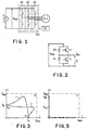
- FIG. 1 of the accompanying drawings shows the block diagram for the generation of variable three-phase alternating voltages applied to an inductive load, such as an electric motor ME, starting from a source E of unidirectional voltage v bus .
- the INV inverter is made up of a certain number of so-called “legs" (legs), equal to the number of phases to be generated, therefore three legs G1, G2, G3 for a three-phase inverter.
- Each leg of the inverter is made using valves made up of semiconductors which fulfill the ideal function.
- the one of a bidirectional switch although the components are per se unidirectional, like the diodes and the transistors, and it is controlled by a control circuit CC which imposes the switching of the transistors (forced switching).
- FIG. 2 shows a typical embodiment of an inverter leg by the use of two transistors T +, T- and two recirculation diodes D +, D-.
- the average value of the output voltage v u can be arbitrarily adjusted between 0 and v bus , by modulating the periods of permanence on the two instantaneous values 0 and v bus , with a switching frequency high enough to limit the current ripples produced by the waveform to two values of the voltage v u .
- Figure 3 shows a typical location vi (voltage-current diagram) for a transistor used in a forced switching circuit.
- the operating area S under safety conditions is ideally determined by the maximum voltage V max as well as by the maximum current I max that the transistor can withstand;
- Ap indicates the opening condition and Co the conduction condition of the transistor;
- line 1 is the diagram of the operating conditions of the transistor during a transition from conduction to opening, and
- line 2 is the diagram of the operating conditions of the transistor during a transition from opening to conduction.
- thyristors cannot be used, which are more robust than transistors in relation to operation in the conduction and opening states, but which cannot switch from conduction to opening only in the absence of any current flowing through them
- FIG. 4 shows the block diagram of a resonant bus power converter supplied by a DC voltage source E, with a LC resonant circuit in series and a non-zero average voltage.
- the legs of the inverter INV do not have switching problems because at each period of oscillation the voltage v bus goes through zero; by choosing these time intervals for performing the switching operations, there is no considerable stress on the semiconductors.
- GTO controlled extinction thyristors
- valves constituting a resonant bus inverter relate to voltage undersizing, because in principle the peak voltage that they must support is greater than or equal to twice the average voltage d which is useful for generating power.
- Figure 5 shows (similarly to Figure 3) a typical location vi for a power valve used in a resonant bus reversing circuit.
- the peak voltage V pk is twice the average voltage V out , useful for power generation. Also in this case, therefore, there is a considerable under-use of semi- conductors.
- the object of the present invention is to improve the power converters of electrical energy, especially for the supply of electric motors, so as to allow obtaining one or more several of the following advantages: obtaining the maximum exploitation of the semiconductors constituting the inverter circuit; obtain the highest reliability and protectability of the system; allow the use of thyristors instead of transistors; eliminate or reduce the need for sophisticated control circuits and protection techniques for circuit protection under fault conditions.
- This object is achieved, according to the invention, in that between the unidirectional electric power source and the voltage reversing circuit is inserted in bypass a system of components arranged to control, in an active and unconditioned manner in the time, the supply voltage of the voltage inverter circuit, in the sense, on the one hand, of limiting the maximum value of the voltage applied to the inverter circuit, and on the other hand of assisting the switching by temporarily canceling (or by temporarily making negative) the supply voltage applied to the inverter circuit, at least in the time intervals in which switches must be made in the inverter circuit.
- said system of components comprises a capacitor connected, through a diode, bypass to the source of voltage. unidirectional sion, a first controlled switch element inserted in bypass to said diode, and a second controlled switch element inserted in a bypass circuit at the input of the inverter circuit.
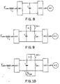
- FIG. 6 there is shown schematically a power converter circuit according to the invention, including the inverting circuit INV (controlling a electric motor ME) is supplied by a DC voltage source E; the supply circuit includes an inductor L.
- This circuit will be described first by neglecting the components EA, DA and SWA, which will be discussed further.
- a system of components comprising a capacitor C connected in bypass to the supply voltage source E through a diode D, a first controlled switch element SW + inserted in bypass said diode D, and a second controlled switch element SW- inserted in bypass at the input of the inverter circuit INV.
- This system of components represents the first essential characteristic of the invention, and it has the function of actively controlling the voltage v bus at the input of the inverter circuit INV between two values 0 and v c , while the mean value of this voltage remains equal to the supply voltage E.
- the function of the capacitor C is, on the one hand, that of absorbing (through the diode D) the excess of the supply voltage with respect to the charging voltage v c of the capacitor. This implies that, by controlling the circuits so as to maintain the charging voltage of the capacitor C within a predetermined maximum limit, surely the application of any voltage substantially greater than the inverter circuit is avoided.
- the function of the capacitor C is also, on the other hand, that of temporarily providing for demands of current i inv absorbed by the inverter circuit, greater than the current i L delivered by the power source. This takes place by the action of the controlled switch SW + whose function is that, when it is in conduction, it allows part of the electrical energy accumulated in the capacitor C to flow towards the inverting circuit INV.
- the function of the controlled switch element SW- is that of establishing a momentary short circuit at the terminals of the input of the inverting circuit INV, thus canceling the voltage v bus which is applied to it.
- v bus 0
- the inverter valves can be switched without stress.
- the dimensioning problems are all displaced on the controlled switch elements SW + and SW-, in a way which depends on the quantitative dimensioning of L and C.
- SW + in the operating conditions it must support the commutations if the differential current (i L -i inv ) has a negative sign; the conduction could be considerable because SW + is in conduction for extended times (almost always); but in practice, because the differential current (i L -i inv ) must be zero on average, the real conduction time of SW + is much more reduced; during the remaining time the current (i L -i inv ) has a positive sign and it then affects the conduction of the diode D. It can be shown that the greater the differential current (i L -i inv ) compared to the one of its more reduced components is the conduction time of SW +.
- the switch elements SW + and SW- must be controlled in a precise manner in order to force the switching operations. Consequently, sophisticated control circuits are necessary for this control, and also switching assistance circuits can be useful, in a manner entirely similar to what is known for controlling the valves of the reversing circuit. On the contrary, by the application of the invention such a necessity does not arise for the inverter valves, which are completely free from switching problems. Because the number of inverter valves is greater than the number (only two) of the switch elements controlled according to the invention, it is possible to obtain a complete conversion structure which is more economical and less dissipative, despite the complication apparent circuits, introduced by the presence of an active control structure of the DC power supply.
- the fault condition to be considered mainly is the short circuit on the load.
- a circuit corresponding to the diagram according to FIG. 6 can have problems only under the conduction conditions of SW +. It is therefore necessary to provide SW + with real-time protection against overcurrent, that is to say a sophisticated and complicated control circuit, substantially according to the known technique. After SW + has been opened you can close SW- and then open the inverter valves to cancel the effects of the short circuit on the load. Then, by reopening SW-, the short-circuit overcurrent transient caused at L is depleted.
- FIG. 6 which is the basic diagram of a power inverter circuit according to the invention, can be improved in a simple manner with the aim of considerably reducing switching losses and making protection easier. of the converter.
- EA source of a reduced voltage compared to the working voltage
- the source EA forms a group with a diode DA, and it can be inserted in parallel with the controlled switch SW- by means of the control of a switch SWA.
- the block constituted by the components EA, DA and SWA is activated by closing SWA before closing SW +, each time the voltage V bus , after having been canceled by SW-, must be restored to its maximum value. The following three phases then take place:
- First phase when SWA is closed, the application of a reduced positive voltage (for example of the order of 10 volts) causes the restoration of the direct polarization of SW- as well as of all the valves forming part of the active legs of the inverter INV, by a lower energy consumption due to the reduced value of the voltage EA.
- a reduced positive voltage for example of the order of 10 volts
- Second phase after obtaining said direct polarization up to the voltage EA, the situation can possibly be controlled by appropriate signaling circuits, to authorize the continuation of the operation only if the polarization is effectively established, while the operation can be blocked otherwise.
- one of the objects of the invention is to allow the use of thyristors instead of the transistors in a forced switching converter.
- the thyristors cannot force the switching operations, and therefore to open one of these components, it is first necessary to cancel the current conduct, wait a certain time and then reapply the voltage across the component. This cannot be done by the basic diagram shown in Figure 6. However, by further development of the basic diagram in Figure 6 the indicated effect can be achieved in an active way according to the criteria of the invention .
- the modified scheme for this purpose is shown in Figure 7 (only for one phase of the AC current delivered), and as can be seen it involves the introduction of an auxiliary voltage produced by a voltage source E aux an appropriate way.
- the auxiliary voltage v aux is capable of producing the natural switching of the thyristors. To extinguish thyristors T +, T-, each having a diode D +, D- connected in antiparallel, it is necessary to bring to an inverted value, even if small, the voltage applied to the thyristors. Referring to in FIG.
- V aux sizing must be done with care, because even small excess errors give rise to high currents in the diodes inserted in antiparallel to the thyristors, while even small faults can prevent extinction. correct thyristors. Indeed the safe extinction is reached when v bus has a value equal to or less than -v d . Therefore v bus , during switching periods, must be between the values -2 v d and -v d . Consequently the factor b of which in the preceding paragraph must be between 1 and 2.
- the voltage v aux can be obtained by means of low voltage circuits controlled so as to adjust v bus according to the condition indicated above.
- a switching circuit supplied by a modulated low voltage can be used to obtain the function of which above.
- the converter is supplied by a unidirectional current, but, in industrial electronics, is of paramount interest the three-phase supply of electric motors by a power obtained from a three-phase network, in general at a frequency of 50 to 60 Hz.
- the invention is particularly suitable for this application, even if and above all when recovery of the mechanical energy from the network is required.
- the characteristic operation according to the invention of the controlled switch elements SW + and SW- intended to assist the switching of the valves included in the inverters, can be controlled on request, namely by intervening each time that the DC control circuits control a switching operation on the inverter circuits, or else this operation can be controlled in cadence with a sufficiently high frequency, and in this case any desired switching is kept on standby until a favorable condition for switching occurs.
Landscapes
- Engineering & Computer Science (AREA)
- Power Engineering (AREA)
- Inverter Devices (AREA)
- Control Of Motors That Do Not Use Commutators (AREA)
- Control Of Stepping Motors (AREA)
- Control Of Electric Motors In General (AREA)
- Stand-By Power Supply Arrangements (AREA)
- Dc-Dc Converters (AREA)
Applications Claiming Priority (2)
| Application Number | Priority Date | Filing Date | Title |
|---|---|---|---|
| IT6751989 | 1989-06-27 | ||
| IT8967519A IT1232122B (it) | 1989-06-27 | 1989-06-27 | Convertitore di potenza di energia elettrica,con commutazione assistita per mezzo di un controllo attivo della tensione di alimentazione del circuito invertitore di tensione |
Publications (3)
| Publication Number | Publication Date |
|---|---|
| EP0405653A2 true EP0405653A2 (de) | 1991-01-02 |
| EP0405653A3 EP0405653A3 (en) | 1991-03-27 |
| EP0405653B1 EP0405653B1 (de) | 1995-04-12 |
Family
ID=11303115
Family Applications (1)
| Application Number | Title | Priority Date | Filing Date |
|---|---|---|---|
| EP90201597A Expired - Lifetime EP0405653B1 (de) | 1989-06-27 | 1990-06-19 | Elektrische Energie-Leistungskonverter, deren Kommutierung durch eine aktive Steuerung der Versorgungsspannung der Spannungsumpolschaltung unterstützt wird |
Country Status (7)
| Country | Link |
|---|---|
| US (1) | US5053938A (de) |
| EP (1) | EP0405653B1 (de) |
| AT (1) | ATE121236T1 (de) |
| DE (1) | DE69018528T2 (de) |
| DK (1) | DK0405653T3 (de) |
| ES (1) | ES2072968T3 (de) |
| IT (1) | IT1232122B (de) |
Families Citing this family (2)
| Publication number | Priority date | Publication date | Assignee | Title |
|---|---|---|---|---|
| CN100338863C (zh) * | 2001-11-05 | 2007-09-19 | 奥地利西门子股份公司 | 电压转换器 |
| KR100784649B1 (ko) * | 2006-04-21 | 2007-12-12 | 경성대학교 산학협력단 | 단상 에스알엠 구동회로 및 구동방법 |
Family Cites Families (14)
| Publication number | Priority date | Publication date | Assignee | Title |
|---|---|---|---|---|
| US3538419A (en) * | 1968-03-25 | 1970-11-03 | Tokyo Shibaura Electric Co | Inverter device |
| DK135478C (da) * | 1972-09-22 | 1977-10-17 | Siemens Ag | Sumslukkeanordning for vekselretterventilerne i en mellemkredsfrekvensomsetter der energiforsyner en elektrisk motor |
| JPS49129827A (de) * | 1973-04-20 | 1974-12-12 | ||
| DE2541700C3 (de) * | 1975-09-18 | 1980-09-11 | Siemens Ag, 1000 Berlin Und 8000 Muenchen | Verfahren zum Betrieb eines Schwingkreisumrichters |
| JPS5953788B2 (ja) * | 1977-10-27 | 1984-12-26 | 株式会社東芝 | インバ−タ装置 |
| US4309751A (en) * | 1978-12-25 | 1982-01-05 | Tokyo Shibaura Denki Kabushiki Kaisha | Method and apparatus for controlling current type inverters |
| DE2937078A1 (de) * | 1979-09-11 | 1981-03-26 | Licentia Gmbh | Selbstgefuehrter weschselrichter mit summenloeschschaltung |
| JPS57170076A (en) * | 1981-04-08 | 1982-10-20 | Mitsubishi Electric Corp | Power invertor |
| JPS57186989A (en) * | 1981-05-12 | 1982-11-17 | Toshiba Corp | Commutation control device of current-type inverter |
| US4567420A (en) * | 1983-05-20 | 1986-01-28 | Ross Hill Controls Corporation | Semi-conductor motor control system |
| DE3347108A1 (de) * | 1983-12-27 | 1985-07-04 | Garbe Lahmeyer & Co Ag | Statische umrichterbruecke |
| US4730242A (en) * | 1986-09-25 | 1988-03-08 | Wisconsin Alumni Research Foundation | Static power conversion and apparatus having essentially zero switching losses |
| FR2613554B1 (fr) * | 1987-03-30 | 1993-05-07 | Telemecanique Electrique | Convertisseur a modulation de largeur d'impulsions |
| US4965709A (en) * | 1989-09-25 | 1990-10-23 | General Electric Company | Switching converter with pseudo-resonant DC link |
-
1989
- 1989-06-27 IT IT8967519A patent/IT1232122B/it active
-
1990
- 1990-06-19 AT AT90201597T patent/ATE121236T1/de not_active IP Right Cessation
- 1990-06-19 DE DE69018528T patent/DE69018528T2/de not_active Expired - Fee Related
- 1990-06-19 DK DK90201597.3T patent/DK0405653T3/da active
- 1990-06-19 ES ES90201597T patent/ES2072968T3/es not_active Expired - Lifetime
- 1990-06-19 EP EP90201597A patent/EP0405653B1/de not_active Expired - Lifetime
- 1990-06-21 US US07/541,497 patent/US5053938A/en not_active Expired - Fee Related
Also Published As
| Publication number | Publication date |
|---|---|
| IT8967519A0 (it) | 1989-06-27 |
| EP0405653A3 (en) | 1991-03-27 |
| DE69018528T2 (de) | 1995-12-14 |
| DK0405653T3 (da) | 1995-08-14 |
| ATE121236T1 (de) | 1995-04-15 |
| ES2072968T3 (es) | 1995-08-01 |
| IT1232122B (it) | 1992-01-23 |
| US5053938A (en) | 1991-10-01 |
| EP0405653B1 (de) | 1995-04-12 |
| DE69018528D1 (de) | 1995-05-18 |
Similar Documents
| Publication | Publication Date | Title |
|---|---|---|
| EP2355331B1 (de) | Wandlervorrichtung und mit einer solchen vorrichtung ausgerüstete unterbrechungslose versorgung | |
| EP0082071B1 (de) | Einrichtung für die Umschaltung einer mit mindestens einem gesteuerten Schalter versehenen Gleichspannungsquelle und Kommutierungshilfsschaltung für eine solche Einrichtung | |
| EP2442436B1 (de) | Verfahren und Steuersystem zur allgemeinen Reduzierung des Stroms in einem Leistungswandler | |
| EP0135672B1 (de) | Ausgleichsschaltung für in Reihe geschaltete Schalter | |
| WO1993002501A1 (fr) | Dispositif electronique de conversion d'energie electrique | |
| WO1981003722A1 (fr) | Onduleur a transistors ou a thyristors a recuperation d'energie | |
| EP0112763A1 (de) | Hochspannungsversorgungseinrichtung für eine Last wie zum Beispiel für einen Röntgengenerator | |
| CA1226653A (fr) | Dispositif d'alimentation d'une charge, notamment un moteur a courant continu pour locomotives ferroviaires du type bi-courant | |
| WO1988007784A1 (fr) | Convertisseur a modulation de largeur d'impulsions | |
| EP2815493A1 (de) | Elektrische ac/dc-umwandlungsvorrichtung zur energierückgewinnung und verwaltung von gleichstromseitigen kurzschlüssen | |
| EP0405653B1 (de) | Elektrische Energie-Leistungskonverter, deren Kommutierung durch eine aktive Steuerung der Versorgungsspannung der Spannungsumpolschaltung unterstützt wird | |
| WO2020136333A1 (fr) | Protection contre les surtensions d'un système de génération d'énergie électrique à vitesse variable et fréquence constante | |
| EP0267252B1 (de) | Frequenzumwandler zur stabilen speisung von asynchronmotoren | |
| EP0670624A1 (de) | Angepasster Schaltnetzteil zur Niederspannungsschaltung | |
| EP3656030A1 (de) | Leistungsflusssteuerungsvorrichtung zur steuerung der verteilung von strömen in einem mesh-netzwerk | |
| EP4315381B1 (de) | Abschaltvorrichtung für elektrischen hochspannungsstrom mit plasmaröhre | |
| EP4382343A1 (de) | Stromversorgungssystem zur versorgung einer elektrischen last mit einer mehrphasigen spannung und einem hilfsnetz durch eine homopolare komponente dieser spannung, zugehörige elektrische anlage | |
| EP1410488B1 (de) | Energieumwandlungseinrichtung | |
| EP0044776B1 (de) | Zerhackerschaltkreis mit freier Kommutierung | |
| CH617549A5 (en) | Electrical power converter | |
| EP1444768A2 (de) | Verfahren und einrichtung zur transformation einer gleichspannung und verwendung der einrichtung | |
| WO2024022713A1 (fr) | Système de conversion tension/courant ou courant/tension | |
| EP0928057B1 (de) | Hochspannungsschalter aus reihengeschalteten resonanten Zellen | |
| EP3888217B1 (de) | System mit einer lösung zur rekonfiguration des anschlusses eines leistungsflussreglers in einem vermaschten netzwerk | |
| CA2504216C (fr) | Appareil et methode pour modifier un ecoulement de puissance dans un troncon d'une ligne de transport d'energie electrique |
Legal Events
| Date | Code | Title | Description |
|---|---|---|---|
| PUAI | Public reference made under article 153(3) epc to a published international application that has entered the european phase |
Free format text: ORIGINAL CODE: 0009012 |
|
| AK | Designated contracting states |
Kind code of ref document: A2 Designated state(s): AT BE CH DE DK ES FR GB LI LU NL SE |
|
| PUAL | Search report despatched |
Free format text: ORIGINAL CODE: 0009013 |
|
| AK | Designated contracting states |
Kind code of ref document: A3 Designated state(s): AT BE CH DE DK ES FR GB LI LU NL SE |
|
| 17P | Request for examination filed |
Effective date: 19910912 |
|
| 17Q | First examination report despatched |
Effective date: 19930506 |
|
| RAP3 | Party data changed (applicant data changed or rights of an application transferred) |
Owner name: FRATTA, ANTONINO, DR.ING. |
|
| GRAA | (expected) grant |
Free format text: ORIGINAL CODE: 0009210 |
|
| AK | Designated contracting states |
Kind code of ref document: B1 Designated state(s): AT BE CH DE DK ES FR GB LI LU NL SE |
|
| REF | Corresponds to: |
Ref document number: 121236 Country of ref document: AT Date of ref document: 19950415 Kind code of ref document: T |
|
| REF | Corresponds to: |
Ref document number: 69018528 Country of ref document: DE Date of ref document: 19950518 |
|
| PGFP | Annual fee paid to national office [announced via postgrant information from national office to epo] |
Ref country code: DK Payment date: 19950626 Year of fee payment: 6 |
|
| PGFP | Annual fee paid to national office [announced via postgrant information from national office to epo] |
Ref country code: LU Payment date: 19950701 Year of fee payment: 6 |
|
| REG | Reference to a national code |
Ref country code: ES Ref legal event code: FG2A Ref document number: 2072968 Country of ref document: ES Kind code of ref document: T3 |
|
| GBT | Gb: translation of ep patent filed (gb section 77(6)(a)/1977) |
Effective date: 19950703 |
|
| REG | Reference to a national code |
Ref country code: DK Ref legal event code: T3 |
|
| PLBE | No opposition filed within time limit |
Free format text: ORIGINAL CODE: 0009261 |
|
| STAA | Information on the status of an ep patent application or granted ep patent |
Free format text: STATUS: NO OPPOSITION FILED WITHIN TIME LIMIT |
|
| 26N | No opposition filed | ||
| PG25 | Lapsed in a contracting state [announced via postgrant information from national office to epo] |
Ref country code: LU Free format text: LAPSE BECAUSE OF NON-PAYMENT OF DUE FEES Effective date: 19960619 Ref country code: DK Effective date: 19960619 |
|
| REG | Reference to a national code |
Ref country code: DK Ref legal event code: EBP |
|
| PGFP | Annual fee paid to national office [announced via postgrant information from national office to epo] |
Ref country code: BE Payment date: 19980605 Year of fee payment: 9 |
|
| PGFP | Annual fee paid to national office [announced via postgrant information from national office to epo] |
Ref country code: AT Payment date: 19980625 Year of fee payment: 9 |
|
| PGFP | Annual fee paid to national office [announced via postgrant information from national office to epo] |
Ref country code: NL Payment date: 19980629 Year of fee payment: 9 |
|
| PGFP | Annual fee paid to national office [announced via postgrant information from national office to epo] |
Ref country code: CH Payment date: 19980724 Year of fee payment: 9 |
|
| PG25 | Lapsed in a contracting state [announced via postgrant information from national office to epo] |
Ref country code: AT Free format text: LAPSE BECAUSE OF NON-PAYMENT OF DUE FEES Effective date: 19990619 |
|
| PG25 | Lapsed in a contracting state [announced via postgrant information from national office to epo] |
Ref country code: LI Free format text: LAPSE BECAUSE OF NON-PAYMENT OF DUE FEES Effective date: 19990630 Ref country code: CH Free format text: LAPSE BECAUSE OF NON-PAYMENT OF DUE FEES Effective date: 19990630 Ref country code: BE Free format text: LAPSE BECAUSE OF NON-PAYMENT OF DUE FEES Effective date: 19990630 |
|
| BERE | Be: lapsed |
Owner name: FRATTA ANTONINO Effective date: 19990630 |
|
| PG25 | Lapsed in a contracting state [announced via postgrant information from national office to epo] |
Ref country code: NL Free format text: LAPSE BECAUSE OF NON-PAYMENT OF DUE FEES Effective date: 20000101 |
|
| REG | Reference to a national code |
Ref country code: CH Ref legal event code: PL |
|
| NLV4 | Nl: lapsed or anulled due to non-payment of the annual fee |
Effective date: 20000101 |
|
| PGFP | Annual fee paid to national office [announced via postgrant information from national office to epo] |
Ref country code: ES Payment date: 20010605 Year of fee payment: 12 |
|
| PGFP | Annual fee paid to national office [announced via postgrant information from national office to epo] |
Ref country code: GB Payment date: 20010612 Year of fee payment: 12 |
|
| PGFP | Annual fee paid to national office [announced via postgrant information from national office to epo] |
Ref country code: SE Payment date: 20010615 Year of fee payment: 12 Ref country code: FR Payment date: 20010615 Year of fee payment: 12 |
|
| PGFP | Annual fee paid to national office [announced via postgrant information from national office to epo] |
Ref country code: DE Payment date: 20010726 Year of fee payment: 12 |
|
| REG | Reference to a national code |
Ref country code: GB Ref legal event code: IF02 |
|
| PG25 | Lapsed in a contracting state [announced via postgrant information from national office to epo] |
Ref country code: GB Free format text: LAPSE BECAUSE OF NON-PAYMENT OF DUE FEES Effective date: 20020619 |
|
| PG25 | Lapsed in a contracting state [announced via postgrant information from national office to epo] |
Ref country code: SE Free format text: LAPSE BECAUSE OF NON-PAYMENT OF DUE FEES Effective date: 20020620 Ref country code: ES Free format text: LAPSE BECAUSE OF NON-PAYMENT OF DUE FEES Effective date: 20020620 |
|
| PG25 | Lapsed in a contracting state [announced via postgrant information from national office to epo] |
Ref country code: DE Free format text: LAPSE BECAUSE OF NON-PAYMENT OF DUE FEES Effective date: 20030101 |
|
| EUG | Se: european patent has lapsed | ||
| GBPC | Gb: european patent ceased through non-payment of renewal fee |
Effective date: 20020619 |
|
| PG25 | Lapsed in a contracting state [announced via postgrant information from national office to epo] |
Ref country code: FR Free format text: LAPSE BECAUSE OF NON-PAYMENT OF DUE FEES Effective date: 20030228 |
|
| REG | Reference to a national code |
Ref country code: FR Ref legal event code: ST |
|
| REG | Reference to a national code |
Ref country code: ES Ref legal event code: FD2A Effective date: 20030711 |