EP0405677A2 - Dispositif électronique supraconducteur à couches minces et procédé pour sa fabrication - Google Patents
Dispositif électronique supraconducteur à couches minces et procédé pour sa fabrication Download PDFInfo
- Publication number
- EP0405677A2 EP0405677A2 EP90201661A EP90201661A EP0405677A2 EP 0405677 A2 EP0405677 A2 EP 0405677A2 EP 90201661 A EP90201661 A EP 90201661A EP 90201661 A EP90201661 A EP 90201661A EP 0405677 A2 EP0405677 A2 EP 0405677A2
- Authority
- EP
- European Patent Office
- Prior art keywords
- layers
- superconductor
- earth metal
- layer
- insulator
- Prior art date
- Legal status (The legal status is an assumption and is not a legal conclusion. Google has not performed a legal analysis and makes no representation as to the accuracy of the status listed.)
- Granted
Links
Images
Classifications
-
- H—ELECTRICITY
- H10—SEMICONDUCTOR DEVICES; ELECTRIC SOLID-STATE DEVICES NOT OTHERWISE PROVIDED FOR
- H10N—ELECTRIC SOLID-STATE DEVICES NOT OTHERWISE PROVIDED FOR
- H10N60/00—Superconducting devices
- H10N60/01—Manufacture or treatment
- H10N60/0268—Manufacture or treatment of devices comprising copper oxide
- H10N60/0296—Processes for depositing or forming copper oxide superconductor layers
-
- H—ELECTRICITY
- H10—SEMICONDUCTOR DEVICES; ELECTRIC SOLID-STATE DEVICES NOT OTHERWISE PROVIDED FOR
- H10N—ELECTRIC SOLID-STATE DEVICES NOT OTHERWISE PROVIDED FOR
- H10N60/00—Superconducting devices
- H10N60/01—Manufacture or treatment
- H10N60/0268—Manufacture or treatment of devices comprising copper oxide
- H10N60/0296—Processes for depositing or forming copper oxide superconductor layers
- H10N60/0408—Processes for depositing or forming copper oxide superconductor layers by sputtering
-
- H—ELECTRICITY
- H10—SEMICONDUCTOR DEVICES; ELECTRIC SOLID-STATE DEVICES NOT OTHERWISE PROVIDED FOR
- H10N—ELECTRIC SOLID-STATE DEVICES NOT OTHERWISE PROVIDED FOR
- H10N60/00—Superconducting devices
- H10N60/01—Manufacture or treatment
- H10N60/0912—Manufacture or treatment of Josephson-effect devices
- H10N60/0941—Manufacture or treatment of Josephson-effect devices comprising high-Tc ceramic materials
-
- H—ELECTRICITY
- H10—SEMICONDUCTOR DEVICES; ELECTRIC SOLID-STATE DEVICES NOT OTHERWISE PROVIDED FOR
- H10N—ELECTRIC SOLID-STATE DEVICES NOT OTHERWISE PROVIDED FOR
- H10N60/00—Superconducting devices
- H10N60/80—Constructional details
- H10N60/85—Superconducting active materials
- H10N60/855—Ceramic superconductors
- H10N60/857—Ceramic superconductors comprising copper oxide
- H10N60/858—Ceramic superconductors comprising copper oxide having multilayered structures, e.g. superlattices
Definitions
- the invention relates to a method for producing multilayer electronic thin-film components with superconductor layers based on single-phase alkaline earth metal-doped metal or rare earth metal oxocuprate mixed crystal layers.
- Oxidic superconductors based on alkaline earth metal-doped metal or rare earth oxocuprates are becoming increasingly important as high-temperature superconductors with transition temperatures> 40 K for the implementation of thin-film components in electronic information technology.
- a strong electron-phonon coupling is responsible for the relatively high superconducting transition temperature of such mixed crystals, which creates optimal conditions for coupling the electron or hole pairs acting as carriers of the superconductivity.
- Thin superconductor layers are used to implement very different electronic components, for example, analog or digital components in multi-layer technology, ribbon cables, resistance elements, capacitive components, inductance elements, tunnel elements are known, which take advantage of the Josephson effect.
- Polycrystalline oxide layers such as Al2O3 or SiO2 layers have proven to be good insulator layers, since no free electrons exist in them.
- a tunnel current through electrically insulating layers can only arise if the insulator layer is sufficiently thin so that single electrons and also electron or hole pairs whose energy is insufficient to jump over a barrier such as an insulator layer can pass through this barrier .
- the production of homogeneous oxide layers of very small thickness is not that easy. It prepares e.g. Difficulties in producing such oxide layers without microscopic holes. For this reason, attempts have already been made in practice to replace the very thin oxide layers with other arrangements.
- the invention has for its object to provide a method with which thin, homogeneous insulator layers can be created on superconductor layers, which on the one hand ensure good electrical insulation at least at the operating temperature of the components and moreover, form a secure diffusion barrier for atoms from the border areas between isolated superconductor layers or the border areas between superconductor layers and other materials involved in the overall layer structure.
- amorphous insulator layers made of electrically insulating material, at least at the operating temperature of the components, and not yet recrystallizing at the temperatures used for the deposition of the superconductor layers, between individual superconductor layers and between areas of the superconductor layers which are adjacent to the superconductor layers and are made of materials other than the superconductor materials be attached.
- amorphous layers made of suitable electrically insulating materials do not show this effect.
- they can be manufactured homogeneously, i.e. without microscopic holes, even with very thin layers.
- amorphous aluminum oxide is used for the insulator layers.
- Alumina has the advantage that it only recrystallizes at temperatures above 1000 o C, so that the deposition of the superconducting material can be carried out with substrate temperatures as are customary for the deposition of alkaline earth-doped metal or rare earth metal oxocuprate layers (up to about 800 o C).
- the small dielectric constant DK and the low values for the loss factor tan ⁇ of Al2O3 are also advantageous.
- aluminum cuprate is used for the insulator layers. This has the advantage that copper losses due to diffusion from the superconducting material in the boundary layer area to the insulator layer are avoided.
- yttrium oxocuprates doped with at least one alkaline earth metal are used for the superconductor layers, it being possible for at least some of the yttrium to be substituted by at least one further rare earth metal.
- bismuth oxocuprates or thallium oxocuprates doped with at least one alkaline earth metal can advantageously also be used for the superconductor layers.
- the superconductor layers are sputtered using high-frequency or direct voltage cathode sputtering at a temperature in the range from approximately 500 ° C. to approximately 800 ° C. Atmosphere separated.
- the insulator layers are also deposited by radio frequency or direct voltage sputtering, but at a temperature which is at most equal to and which is preferably lower than the temperature required for the deposition of the superconductor layers.
- a cathode sputtering system which enables the changing of targets during the coating process is advantageously used to carry out these processes. It is advantageous to use a rotatable substrate holder, with magnetron sputtering systems being particularly suitable and with control and regulating devices for the pressure of the gas atmosphere and the substrate temperature.
- the method according to the invention can advantageously be used for the production of multilayer analog or digital components.
- SQUIDs Superconducting Quantum Interference Devices
- SQUIDs can also be used as amplifiers or as digital components, for example for logic operations or as storage elements.
- connection lines in superconducting circuits are designed as ribbon or strip lines, which are formed on a substrate with an insulator layer attached thereon.
- the method according to the invention can also be used for the production of resistance elements, for example cross cryotrons or parallel cryotrons.
- the substrate and the layer support consist, for example, of single crystal disks made of aluminum oxide (sapphire), magnesium oxide, zirconium dioxide, strontium titanate or lithium niobate.
- a superconducting base layer on it, which remains superconducting in all operating states of the cryotron and must therefore have high critical temperatures T c and high critical field strengths.
- Insulator layers made of an electrically insulating material are required to isolate the superconducting layer.
- a superconducting layer which acts as a gate conductor, is applied as the active element of the cryotron, which layer can assume both the superconducting and the normal conducting state when the cryotron is in operation.
- an insulator layer is attached to the superconductor layer, which acts as a gate conductor, on which another superconducting layer, which acts as a control conductor, is attached.
- the control conductor remains superconducting in all operating states of the cryotron and is therefore made of the same material as the superconducting base layer.
- a Ryotron is a superconducting component with a pronounced non-linear inductance. It consists of two superconducting layers that act as control conductors, between which there is another superconducting layer that acts as gate conductor. The superconducting layers are insulated from one another by insulator layers. The gate conductor remains superconducting during operation of the ryotron. Its inductance change takes place through Formation of a magnetic field surrounding it with the help of the control conductors, which can assume the normal or superconducting state.
- the magnetic properties of thin superconducting and thin magnetic layers are used in cryactuators. There is a thin ferromagnetic layer on a superconducting base layer, over which, as with a cross cryotron, thin superconducting layers, which act as gate and control conductors and which are electrically insulated from each other by insulator layers, cross each other.
- the superconducting layer acting as a control conductor is arranged parallel to the axis of easy magnetization of the ferromagnetic layer, the magnetization vector being able to be rotated in the layer plane with the aid of the control current, which results in a change in the inductance of the gate conductor without the control or gate conductor in the normal conductor State can be switched.
- the gate current With the gate current, however, magnetic fields are generated in the same direction or opposite to the direction of magnetization. A sufficiently large magnetic field opposite to the direction of easy magnetization leads the magnetization vector in this direction, which is also stable. In this way, two defined states can be set, to which the values 0 and 1 of a memory element can be assigned.
- the method according to the invention can also be used for the production of tunnel elements.
- Components with at least partially superconducting electrodes and single-electron tunnels correspond to the analog components of semiconductor technology. These components can have non-linear current-voltage characteristics that are set via the structure of the layer package of the tunnel junction.
- the insulator layer of the tunnel junction usually has a thickness in the range up to a few 10 nm
- the ribbon cables usually have a thickness in the range up to 300 nm and a width in the range up to 500 ⁇ m.
- a special form of tunnel elements are Josephson tunnel elements.
- the tunnel transition represents the non-linear gate conductor, which is controlled by a magnetic field.
- all parts of the Josephson junction remain superconducting during the switching process.
- the tunneling of the electron or hole pairs through the insulator layer which is very thin in the case of these components, is converted into simple electron tunneling at high currents, as a result of which a voltage jump occurs at the Josephson junction.
- insulator layers for superconducting electronic thin-film components can be produced which are homogeneous and which, in addition to their effect as good electrical insulators, in particular at the operating temperature of the components, also have the advantage of providing a diffusion barrier for the to form relatively high temperatures at which the superconducting layers are usually deposited.
- the insulator layers according to the invention are used, for example, on non-oxidized, optionally doped silicon single-crystal substrates, as used in semiconductor technology technology, separated, there is a combination of advantages: the insulator layer not only acts as a diffusion barrier and as a good electrical insulator, but also the lower values for the dielectric constant DK and the lower values for the dissipation factor tan ⁇ advantageous.
- amorphous insulator layers according to the invention in comparison to the known polycrystalline insulator layers is their morphology: amorphous layers are better suited for protecting these surfaces against environmental influences, for example as a protection against, because of the more homogeneous covering of the surfaces carrying them than a layer with a polycrystalline structure Superconductor layers against influences that impair their superconductivity, such as loss of oxygen or the chemical decomposition of the superconductor layer under the influence of water vapor from the atmosphere.
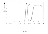
- the figure shows an Auger depth profile of a manufactured according to the inventive method YBa2CU3O x - Al2O3 - YBa2Cu3O x - layer sequence.
- Thin superconducting layers based on single-phase YBa2Cu3O x mixed crystals were produced by high-frequency sputtering of ceramic targets. MgO single crystal wafers oriented in the [100] direction were used as the substrate. To produce a multilayer structure, insulator layers made of amorphous Al2O3 were produced by DC sputtering on the superconductor layer.
- a cathode sputtering system was used to carry out the process, which enables the changing of targets during the coating cycle. For this reason, the substrate holder in the cathode sputtering system was made rotatable and a possibility was provided to mount a maximum of 4 targets.
- the pressure of the atomizing gas atmosphere and the substrate temperature were continuously checked or regulated during the layer deposition process. Both metallic aluminum and aluminum oxide can be used as the target for the insulator layers. In the former case, the sputtering process must be carried out in a reactive gas phase, i.e. Pure oxygen is used as the atomizing gas. If an aluminum oxide target is used, it is expedient to work with an inert gas / oxygen gas atmosphere.
- the YBa2Cu3O x superconductor layer was produced using the following parameters: Target YBa2Cu3O x , sintered Substrate MgO, oriented in the [100] direction Substrate temperature 580 to 600 oC Inert gas pressure (e.g. argon) 6 Pa Oxygen pressure 4 Pa Power area density 4 W / cm2 high-frequency power (13.56 MHz) Separation rate 0.07 nm / s Layer thickness 500 nm.
- Al2O3 insulator layer was carried out with the following parameters: Target aluminum Substrate MgO, oriented in the [100] direction / superconducting YBa2Cu3O x layer Substrate temperature 580 to 600 oC Inert gas pressure - Oxygen pressure 1.1 Pa Power area density 2 W / cm2 DC power Separation rate 0.035 nm / s Layer thickness 170 nm.
- the insulator layer has been deposited with a layer thickness of 170 nm.
- the layer thickness of the insulator layer it is possible to adapt the layer thickness of the insulator layer to the desired conditions and it can also be deposited in smaller layer thicknesses accordingly.
Landscapes
- Engineering & Computer Science (AREA)
- Manufacturing & Machinery (AREA)
- Chemical & Material Sciences (AREA)
- Ceramic Engineering (AREA)
- Superconductor Devices And Manufacturing Methods Thereof (AREA)
- Superconductors And Manufacturing Methods Therefor (AREA)
- Physical Vapour Deposition (AREA)
- Inorganic Compounds Of Heavy Metals (AREA)
Applications Claiming Priority (2)
| Application Number | Priority Date | Filing Date | Title |
|---|---|---|---|
| DE3921363 | 1989-06-29 | ||
| DE3921363A DE3921363A1 (de) | 1989-06-29 | 1989-06-29 | Verfahren zur herstellung von supraleitenden elektronischen duennschichtbauelementen |
Publications (3)
| Publication Number | Publication Date |
|---|---|
| EP0405677A2 true EP0405677A2 (fr) | 1991-01-02 |
| EP0405677A3 EP0405677A3 (en) | 1991-04-17 |
| EP0405677B1 EP0405677B1 (fr) | 1995-09-06 |
Family
ID=6383902
Family Applications (1)
| Application Number | Title | Priority Date | Filing Date |
|---|---|---|---|
| EP90201661A Expired - Lifetime EP0405677B1 (fr) | 1989-06-29 | 1990-06-25 | Dispositif électronique supraconducteur à couches minces et procédé pour sa fabrication |
Country Status (4)
| Country | Link |
|---|---|
| EP (1) | EP0405677B1 (fr) |
| JP (1) | JPH0338075A (fr) |
| KR (1) | KR910002026A (fr) |
| DE (2) | DE3921363A1 (fr) |
Cited By (1)
| Publication number | Priority date | Publication date | Assignee | Title |
|---|---|---|---|---|
| CN114600262A (zh) * | 2019-10-24 | 2022-06-07 | 微软技术许可有限责任公司 | 半导体超导体混合器件 |
Families Citing this family (2)
| Publication number | Priority date | Publication date | Assignee | Title |
|---|---|---|---|---|
| JP2007167366A (ja) * | 2005-12-22 | 2007-07-05 | Teijin Ltd | 神経再生材料 |
| DE102020213680A1 (de) | 2020-10-30 | 2022-05-05 | Forschungszentrum Jülich GmbH | Verfahren zum Sintern keramischer Werkstoffe |
Family Cites Families (3)
| Publication number | Priority date | Publication date | Assignee | Title |
|---|---|---|---|---|
| JPS63266889A (ja) * | 1987-04-24 | 1988-11-02 | Hitachi Ltd | ジヨセフソン接合装置 |
| JPS6431475A (en) * | 1987-07-28 | 1989-02-01 | Univ Tokyo | Superconducting device and forming method thereof |
| JPS6441281A (en) * | 1987-08-07 | 1989-02-13 | Canon Kk | Josephson element |
-
1989
- 1989-06-29 DE DE3921363A patent/DE3921363A1/de not_active Withdrawn
-
1990
- 1990-06-25 EP EP90201661A patent/EP0405677B1/fr not_active Expired - Lifetime
- 1990-06-25 DE DE59009608T patent/DE59009608D1/de not_active Expired - Fee Related
- 1990-06-26 JP JP2165819A patent/JPH0338075A/ja active Pending
- 1990-06-27 KR KR1019900009525A patent/KR910002026A/ko not_active Withdrawn
Cited By (2)
| Publication number | Priority date | Publication date | Assignee | Title |
|---|---|---|---|---|
| CN114600262A (zh) * | 2019-10-24 | 2022-06-07 | 微软技术许可有限责任公司 | 半导体超导体混合器件 |
| US12082512B2 (en) | 2019-10-24 | 2024-09-03 | Microsoft Technology Licensing, Llc | Semiconductor-superconductor hybrid device |
Also Published As
| Publication number | Publication date |
|---|---|
| EP0405677B1 (fr) | 1995-09-06 |
| KR910002026A (ko) | 1991-01-31 |
| DE59009608D1 (de) | 1995-10-12 |
| JPH0338075A (ja) | 1991-02-19 |
| EP0405677A3 (en) | 1991-04-17 |
| DE3921363A1 (de) | 1991-01-10 |
Similar Documents
| Publication | Publication Date | Title |
|---|---|---|
| DE3856452T2 (de) | Herstellungsmethode für ein supraleitendes Bauelement | |
| DE3876473T2 (de) | Verfahren zur herstellung von supraleitenden quanteninterferometern aus hochtemperatur-supraleitern. | |
| DE3850580T2 (de) | Supraleiteranordnung. | |
| DE69119022T2 (de) | Supraleitende Einrichtung mit ultradünnem Kanal aus oxydisch supraleitendem Material und Verfahren zu deren Herstellung | |
| DE68924630T2 (de) | Hochfrequenz-Substrat-Material für Dünnschichtlagen perovskitischer Supraleiter. | |
| DE102004048646B4 (de) | Supraleitende Strombegrenzereinrichtung vom resistiven Typ mit bandförmiger Hoch-Tc-Supraleiterbahn | |
| DE69115209T2 (de) | Verfahren zur Herstellung eines Supraleitungsbauelements mit reduzierter Dicke der supraleitenden Oxidschicht und dadurch hergestelltes Supraleitungsbauelement. | |
| DE68927925T2 (de) | Supraleitender Transistor | |
| DE69119190T2 (de) | Supraleitende Einrichtung mit extrem dünnen supraleitenden Kanal aus oxydischem supraleitendem Material und Methode zu deren Herstellung | |
| DE69132972T2 (de) | Supraleitender Feldeffekttransistor mit inverser MISFET-Struktur und Verfahren zu dessen Herstellung | |
| DE69218348T2 (de) | Supraleitendes Bauelement mit extrem dünnen supraleitenden Kanal und Herstellungsverfahren | |
| DE3878884T2 (de) | Josephson-einrichtung, bestehend aus einer josephson-uebergangsstruktur, welche fuer einen oxidsupraleiter geeignet ist. | |
| DE69015721T2 (de) | Verfahren zur Herstellung einer supraleitenden Schaltung. | |
| DE69123271T2 (de) | Einrichtung mit gestapeltem Josephson-Übergang aus Oxid-Supraleiter Material | |
| DE68918746T2 (de) | Halbleitersubstrat mit dünner Supraleiterschicht. | |
| DE3888341T2 (de) | Halbleitersubstrat mit einem supraleitenden Dünnfilm. | |
| US5250506A (en) | Superconductive switching element with semiconductor channel | |
| DE68923325T2 (de) | Josephson-Einrichtung. | |
| EP0405677B1 (fr) | Dispositif électronique supraconducteur à couches minces et procédé pour sa fabrication | |
| DE69025237T2 (de) | Supraleitende Mehrlagen-Schaltung und Verfahren zu deren Herstellung | |
| DE69223371T2 (de) | Supraleitende Dünnschicht aus oxidisch supraleitendem Material, supraleitender Strompfad und supraleitende Einrichtung mit der supraleitenden Dünnschicht | |
| DE69112775T2 (de) | Verbesserte Konstruktion von Hochtemperatur Supraleiter Übergangsanordnungen. | |
| DE69125456T2 (de) | Verfahren zur Herstellung einer supraleitenden Einrichtung mit reduzierter Dicke der supraleitenden Schicht und dadurch erzeugte supraleitende Einrichtung | |
| DE69116471T2 (de) | Aktive Einrichtung mit oxydischem Supraleiter und deren Herstellungsprozess | |
| DE69219816T2 (de) | Supraleitende Dünnschicht mit mindestens einer isolierten Region, gebildet aus oxydisch supraleitendem Material und Verfahren zu ihrer Herstellung |
Legal Events
| Date | Code | Title | Description |
|---|---|---|---|
| PUAI | Public reference made under article 153(3) epc to a published international application that has entered the european phase |
Free format text: ORIGINAL CODE: 0009012 |
|
| AK | Designated contracting states |
Kind code of ref document: A2 Designated state(s): DE FR GB NL |
|
| PUAL | Search report despatched |
Free format text: ORIGINAL CODE: 0009013 |
|
| RHK1 | Main classification (correction) |
Ipc: H01L 39/22 |
|
| AK | Designated contracting states |
Kind code of ref document: A3 Designated state(s): DE FR GB NL |
|
| 17P | Request for examination filed |
Effective date: 19911014 |
|
| 17Q | First examination report despatched |
Effective date: 19930923 |
|
| GRAA | (expected) grant |
Free format text: ORIGINAL CODE: 0009210 |
|
| AK | Designated contracting states |
Kind code of ref document: B1 Designated state(s): DE FR GB NL |
|
| PG25 | Lapsed in a contracting state [announced via postgrant information from national office to epo] |
Ref country code: NL Free format text: LAPSE BECAUSE OF FAILURE TO SUBMIT A TRANSLATION OF THE DESCRIPTION OR TO PAY THE FEE WITHIN THE PRESCRIBED TIME-LIMIT Effective date: 19950906 |
|
| REF | Corresponds to: |
Ref document number: 59009608 Country of ref document: DE Date of ref document: 19951012 |
|
| GBT | Gb: translation of ep patent filed (gb section 77(6)(a)/1977) |
Effective date: 19951212 |
|
| ET | Fr: translation filed | ||
| NLV1 | Nl: lapsed or annulled due to failure to fulfill the requirements of art. 29p and 29m of the patents act | ||
| PGFP | Annual fee paid to national office [announced via postgrant information from national office to epo] |
Ref country code: GB Payment date: 19960603 Year of fee payment: 7 |
|
| PGFP | Annual fee paid to national office [announced via postgrant information from national office to epo] |
Ref country code: FR Payment date: 19960626 Year of fee payment: 7 |
|
| PLBE | No opposition filed within time limit |
Free format text: ORIGINAL CODE: 0009261 |
|
| STAA | Information on the status of an ep patent application or granted ep patent |
Free format text: STATUS: NO OPPOSITION FILED WITHIN TIME LIMIT |
|
| 26N | No opposition filed | ||
| PG25 | Lapsed in a contracting state [announced via postgrant information from national office to epo] |
Ref country code: DE Effective date: 19970301 |
|
| PG25 | Lapsed in a contracting state [announced via postgrant information from national office to epo] |
Ref country code: GB Free format text: LAPSE BECAUSE OF NON-PAYMENT OF DUE FEES Effective date: 19970625 |
|
| GBPC | Gb: european patent ceased through non-payment of renewal fee |
Effective date: 19970625 |
|
| PG25 | Lapsed in a contracting state [announced via postgrant information from national office to epo] |
Ref country code: FR Free format text: LAPSE BECAUSE OF NON-PAYMENT OF DUE FEES Effective date: 19980227 |
|
| REG | Reference to a national code |
Ref country code: FR Ref legal event code: ST |
|
| REG | Reference to a national code |
Ref country code: FR Ref legal event code: ST |