EP0406524B1 - Mehrnormen-Bildschirmanzeige in einem Fernsehempfänger - Google Patents
Mehrnormen-Bildschirmanzeige in einem Fernsehempfänger Download PDFInfo
- Publication number
- EP0406524B1 EP0406524B1 EP90104634A EP90104634A EP0406524B1 EP 0406524 B1 EP0406524 B1 EP 0406524B1 EP 90104634 A EP90104634 A EP 90104634A EP 90104634 A EP90104634 A EP 90104634A EP 0406524 B1 EP0406524 B1 EP 0406524B1
- Authority
- EP
- European Patent Office
- Prior art keywords
- signal
- horizontal
- circuitry
- vertical
- display
- Prior art date
- Legal status (The legal status is an assumption and is not a legal conclusion. Google has not performed a legal analysis and makes no representation as to the accuracy of the status listed.)
- Expired - Lifetime
Links
- 230000003111 delayed effect Effects 0.000 claims description 21
- 230000001360 synchronised effect Effects 0.000 claims description 14
- 238000000034 method Methods 0.000 claims description 2
- 238000010586 diagram Methods 0.000 description 8
- 238000001514 detection method Methods 0.000 description 7
- 230000000750 progressive effect Effects 0.000 description 2
- 230000002093 peripheral effect Effects 0.000 description 1
- 239000004065 semiconductor Substances 0.000 description 1
Images


Classifications
-
- H—ELECTRICITY
- H04—ELECTRIC COMMUNICATION TECHNIQUE
- H04N—PICTORIAL COMMUNICATION, e.g. TELEVISION
- H04N5/00—Details of television systems
- H04N5/44—Receiver circuitry for the reception of television signals according to analogue transmission standards
- H04N5/445—Receiver circuitry for the reception of television signals according to analogue transmission standards for displaying additional information
-
- H—ELECTRICITY
- H04—ELECTRIC COMMUNICATION TECHNIQUE
- H04N—PICTORIAL COMMUNICATION, e.g. TELEVISION
- H04N5/00—Details of television systems
- H04N5/44—Receiver circuitry for the reception of television signals according to analogue transmission standards
- H04N5/445—Receiver circuitry for the reception of television signals according to analogue transmission standards for displaying additional information
- H04N5/44504—Circuit details of the additional information generator, e.g. details of the character or graphics signal generator, overlay mixing circuits
-
- H—ELECTRICITY
- H04—ELECTRIC COMMUNICATION TECHNIQUE
- H04N—PICTORIAL COMMUNICATION, e.g. TELEVISION
- H04N9/00—Details of colour television systems
- H04N9/64—Circuits for processing colour signals
- H04N9/641—Multi-purpose receivers, e.g. for auxiliary information
Definitions
- the present invention pertains to a television receiver including a microprocessor (MPU) and an on-screen display (OSD) and more particularly to a multistandard OSD including display positioning capabilities.
- MPU microprocessor
- OSD on-screen display
- an MPU is utilized to control all of the functions, e.g. color, synchronization, etc.
- An additional chip which contains all of the OSD circuitry, is coupled to the MPU and provides any on-screen displays.
- Each prior art OSD chip is designed to operate with a specific television receiver, that is, it operates at one specific standard.
- Typical world standards in the television industry include NTSC, PAL, and SECAM.
- multidefinitions which multidefinitions include: improved definition TV (IDTV); extended definition TV (EDTV); high definition (HDTV); as well as interlace scan and progressive scan.
- each chip operates on only one standard, the frequencies within the chip are constant and it is relatively simple to provide features such as horizontal positioning. However, if a different standard signal including different horizontal and vertical frequencies is received, these features can be extremely complex.
- multistandard on screen display circuitry for positioning a picture on the display screen in a television receiver in dependence on the standard of the received TV signal
- a master clock generator for generating a master clock signal synchronised with the horizontal frequency of a received television signal
- horizontal position circuitry adjustable to start horizontal lines of a display at a plurality of predetermined positions in dependence on the standard of a received television signal, the horizontal position circuitry comprising; a counter synchronized with the horizontal frequency of the received television signal, said counter being connected to count pulses of the master clock signal and supply an output signal indicative of the count
- a plurality of input gates for receiving multistandard signals indicative of a plurality of predetermined horizontal line starting positions associated with said standard, for receiving a control signal indicative of the respective standard of the received television signal and for providing in response to the control signal an output signal indicative of a predetermined horizontal line starting position associated with the standard of the received TV signal
- a comparator having first input terminals connected to receive the output
- a method of horizontally positioning a display in a television receiver is also disclosed and claimed in claim 9.
- the preferred embodiment also includes circuitry for providing vertical positioning if desired.
- multistandard television receiver is illustrated embodying the present invention.
- the term "multistandard” refers to the various world standard television systems (e.g. NTSC, PAL, SECAM, etc.) as well as any or all of the various multidefinition systems (IDTV, EDTV, HDTV, interlace scan, progressive scan, etc.).
- IDTV various multidefinition systems
- EDTV various multidefinition systems
- HDTV interlace scan
- progressive scan progressive scan
- An on screen display is produced by dividing each field into a plurality of pixels positioned in horizontal rows and vertical columns.
- Each pixel in turn is composed of dots positioned in horizontal lines and vertical lines. Each dot in each pixel is addressed by horizontal and vertical lines and each pixel is addressed by vertical columns and horizontal rows. The addresses are used to generate the desired display. While the above nomenclature will be used throughout this description it should be understood that this is simply for convenience of description and is not intended to limit the invention in any way.
- the television receiver includes an antenna 10, a tuner 11, IF strip 12, color docoder 13, CRT 14, and MPU 15.
- MPU 15 controls the channel (or operating frequency), the color of the display, and all other controllable features such as brightness, volume, etc.
- a remote unit 16 communicates with MPU 15 for remote control of many controllable features. Only the basic components are illustrated in FIG.1 and many well known peripheral components have been omitted for simplicity.
- FIG.2 illustrates a more detailed block diagram of MPU 15 with the various components, which in this specific embodiment are all formed on a single semiconductor chip.
- FIG.2 also illustrates inputs and outputs to MPU 15, many of which will not be described in detail herein because they are well known to those skilled in the art.
- the main components of MPU 15 to be discussed herein are a CPU 17 and specific circuitry within the multistandard on-screen display (OSD) circuitry 20.
- OSD multistandard on-screen display
- Circuitry 20 includes a phase-locked loop (PLL) 21, a system/mode detection circuit 22, horizontal and vertical counters 24 and 25, respectively, horizontal and vertical position delay circuits 26 and 27, respectively, a 64 character ROM 28, and an MPU interface 30.
- PLL 21 is utilized to synchronize OSD circuitry 20 to any received standard television signal.
- the leading edge of the horizontal flyback pulse portion of a received television signal is used to synchronize PLL 21 to the received television signal.
- the horizontal flyback pulse is also supplied to system/mode detection circuit 22. Master clock signals and horizontal frequency signals from PLL 21 are applied to horizontal counter 24. A third signal synchronized to the horizontal flyback pulses is applied to the vertical counter from PLL 21.
- System/mode detection circuit 22 supplies flags (e.g. mode flag) to PLL 21, horizontal position delay 26, horizontal and vertical counters 24 and 25, and MPU interface 30.
- Horizontal counter 24 supplies dot and column addresses to horizontal position delay circuitry 26, MPU interface 30, and other portions of the circuitry not shown herein.
- Vertical counter 25 supplies line and row addresses to ROM 28 and MPU interface 30.
- Vertical position decay circuitry 27 receives vertical flyback pulses from the standard television signal and supplies a delayed vertical flyback signal to system/mode detection circuit 22 and to vertical counter 25.
- ROM 28 receives signals from MPU interface 30 and supplies signals to remaining portions of OSD circuitry 20 (not illustrated) to generate the predetermined on-screen display.
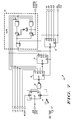
- Horizontal position delay circuit 26 embodying a part of the present invention is illustrated schematically.
- Horizontal position delay circuit 26 includes a counter 35, a comparator 37 and input gates 39.
- Counter 35 includes a first stage 40 and a second stage 41, each of which is constructed to divide an incoming clock signal by 2, 4, 8 and 16.
- the incoming clock signal applied to first stage 40 is obtained from horizontal direction counter 24, as will be explained presently.
- the divide by 16 output of first stage 40 is supplied as a clock input to second stage 41.
- the four outputs of first stage 40 and the four outputs of second stage 41 are applied to a first 8 inputs of comparator 37.
- Counter 35 also includes a D-type flipflop 43 having the output thereof connected to the reset inputs of first stage 40 and second stage 41.
- the clock input of flipflop 43 is connected to receive a horizontal frequency signal M15 which is in phase with the master clock and its derivative signals and synchronized with the horizontal flyback pulses of a received television signal by PLL 21.
- the signal applied to the clock input of flipflop 43 will be at a frequency of approximately 15 KHz or approximately 31 KHz, depending upon the television signal being received.
- Input gates 39 include a first four gates 45 having signal terminals connected to an input terminal 46 and control terminals connected to an input terminal 47 and a second four gates 48 having signal terminals connected to an input terminal 49 and control terminals connected to an input terminal 50.
- Input terminal 46 is connected to receive a 4 bit signal indicative of a predetermined horizontal line starting position when the received telelvison signal has approximately 31 KHz horizontal frequency and input terminal 49 is connected to receive a 4 bit signal indicative of the predetermined horizontal line starting position when the received television signal has approximately a 15 KHz horizontal frequency.
- Input terminals 47 and 50 are connected to receive an inverted mode flag and a mode flag, respectively, from system/mode detection circuit 22, which signals open gates 45 or 48 to allow the proper horizontal frequency signal to pass therethrough.
- the outputs of the four gates 45 and the four gates 48 are connected to the first four of a second eight inputs of comparator 37. The remaining four of the second eight inputs are connected to ground.
- An output of comparator 37 is supplied at an output terminal 51.
- PLL 21 and system/mode detection circuit 22 are synchronized with the horizontal flyback pulse of the received television signal. Because of this synchronization, as is explained more fully in the above described co-pending application, the pulse width of the horizontal flyback pulses affects the horizontal position of the display characters generated by OSD 20. Since the pulse width of the horizontal flyback pulses affects the horizontal position of the display characters, it is required to generate a fixed length pulse from the input horizontal flyback pulse. This fixed length pulse, herein referred to as the delayed horizontal flyback pulse, must be correctly delayed from the input horizontal flyback pulse so that the character display position is aligned correctly on the screen.
- a signal representative of a central bit (DC2) in the address of each pixel in the horizontal line is supplied to the clock input of first stage 40 of counter 35. Because the D-flipflop 43, which is receiving the horizontal frequency at the clock input thereof, resets counter 35 each horizontal line, counter 35 is essentially counting the pixels in each horizontal line.
- comparator 37 By providing at terminal 46 a signal representative of a predetermined position for a 31 KHz horizontal frequency and at terminal 49 a signal for a 15 KHz horizontal frequency, comparator 37 essentially selects the desired pixel in the horizontal line at which the display will begin and provides an output pulse representative thereof. This output pulse from comparator 37 is the delayed horizontal flyback pulse which appears at output terminal 51.
- Horizontal direction counter 24 includes four stages 55, 56, 57 and 58.
- stages 55 and 56 serve as a pixel counter while stages 57 and 58 serve as a column counter.
- a pair of input gates 60 and 61 are operated by the mode flag and the inverted mode flag, respectively, to provide either master clock frequency 7 MHz or master clock frequency 14 MHz (depending upon the received television signal) to the clock input of first stage 55.
- a D-flipflop 63 is connected to receive the synchronized horizontal frequency signal M15 from PLL 21 at the clock input thereof. The output of D-flipflop 63 is connected to the reset of first stage 55 and synchronizes first stage 55 to the horizontal frequency.
- first stage 55 counts the number of dots in a horizontal line.
- First stage 55 divides the input signal by 2, 4 and 8 and these outputs represent 3 bits in the address of the dots in each pixel.
- the third output of first stage 55 is also supplied to the clock input of second stage 56, which divides the clock input by 2 and provides this signal at an output as a fourth (most significant) bit in the dot addresses as well as supplying the signal to the clock input of third stage 57.
- Third stage 57 divides the clock input by 2, 4 and 8 and supplies these signals to three output terminals representing the first 3 bits in a column address.
- the third output of third stage 57 is supplied to the clock input of fourth stage 58 which divides the signal by 2 and 4 and supplies these outputs to two terminals representing the last 2 bits of the column address.
- second stage 56, third stage 57 and fourth stage 58 are reset by the delayed horizontal flyback signal from output terminal 51 of horizontal position delay circuit 26.
- the dot and column addresses are utilized in other circuits of OSD circuitry 20 to accurately generate desired displays at selected positions on the screen of the television.
- vertical position delay circuit 27 is essentially similar to horizontal position delay circuit 26, except that a counter 65 includes three stages connected to count a horizontal frequency signal supplied by PLL 21. All three of the stages of counter 65 are reset by an output from a D-flipflop 66, which is clocked by vertical flyback pulses from the received television signal. As in horizontal position delay circuit 26, the outputs of counter 65 are supplied to one input of a comparator 68 which compares the count to a predetermined word to generate a delayed vertical flyback pulse on an output terminal 69.
- the predetermined word supplied to the second inputs of comparator 68 includes a pair of terminals connected to a high voltage with the remaining terminals connected to ground so that the vertical display always begins at the same position regardless of the type of television signal being received. It will of course be understood that any other word might be applied to the second input terminals of comparator 68 to begin the vertical display at any selected position.
- vertical direction counter 25 is illustrated schematically.
- Vertical direction counter 25 includes a three stage counter 80, 81 and 82.
- An input D-type flipflop 85 is connected to receive the horizontal frequency signal from PLL 21 at the clock input thereof, which signal is also supplied through an inverter to a NAND gate 86.
- Flipflop 85 is set by a height signal which is a high (1) or low (0) signal.
- the characters of the display can be provided with a double height in which case the height signal sets flipflop 85 and the row count is slowed down by one half.
- the output of flipflop 85 is supplied to a second input of NAND gate 86.
- the output signals from NAND gate 86 are supplied at the clock input of first stage 80.
- First stage 80 divides the clock input signal by 2, 4, 8 and 16, all four of which are supplied as the first four bits of a line address signal.
- the fourth output of first stage 80 is supplied as a clock input to second stage 81, which divides the clock input by 2 and supplies this output as the fifth bit of a line address signal.
- the output of second stage 81 is also supplied as an input to a gate 90 along with the delayed vertical flyback pulses from vertical position delay circuit 27 and an inverted system flag 1 signal from system/mode detection circuit 22.
- An output signal from gate 90 is supplied as a clock input to third stage 82 and as a reset to first stages 80 and 81.
- Third stage 82 divides the clock input by 2, 4, 8 and 16 and supplies these four output signals as row address signals in each line.
- the inverted system flag 1 signal supplied to gate 90 controls gate 90 in accordance with the vertical frequency of the television signal being received.
- the delayed vertical flyback signal is supplied to an OR gate in gate 90 and to the reset of third stage 82 so that the row address provided by third stage 82 starts only when the vertical display begins. Further, an inverted delayed vertical flyback signal is applied to the reset of D-flipflop 85 to ensure that line counting by first and second stages 80 and 81 begins with the beginning of the vertical display.
- the line and row addresses are utilized in other circuits of OSD circuitry 20 in conjunction with dot and column addresses to accurately generate desired displays at selected positions on the television screen.
- a television receiver with microprocessor and multistandard OSD circuitry which OSD circuitry includes predetermined selectable horizontal and/or vertical positioning of the display. Further, this selectable positioning of the horizontal and/or vertical display operates automatically with a multistandard OSD circuit.
- the positioning circuitry is relatively simple to construct and is synchronized to the received television signal so that it is accurate and stable.
Landscapes
- Engineering & Computer Science (AREA)
- Multimedia (AREA)
- Signal Processing (AREA)
- Computer Graphics (AREA)
- Controls And Circuits For Display Device (AREA)
- Details Of Television Scanning (AREA)
- Studio Circuits (AREA)
- Television Systems (AREA)
- Synchronizing For Television (AREA)
Claims (9)
- Mehrnormen-Bildschirmanzeigen-Schaltung (20) zum Positionieren eines Bildes an dem Bildschirm eines Fernsehempfängers in Abhangigkeit von der Norm des empfangenen Fernsehsignals, welche Schaltung umfaßt:
einen Haupttakt-Generator (21) zum Erzeugen eines mit der Horizontalfrequenz eines empfangenen Fernsehsignals synchronisierten Haupttaktsignals;
eine Horizontalpositions-Schaltung (24,26), die zum Starten von horizontalen Zeilen einer Anzeige an einer Vielzahl vorgegebener Positionen einstellbar ist in Abhangigkeit von der Norm des empfangenen Fernsehsignals, wobei die Horizontalpositions-Schaltung umfaßt:
einen mit der Horizontalfrequenz des empfangenen Fernsehsignals synchronisierten Zahler (35), der zum Zahlen von Impulsen des Haupttaktsignals und zum Zuführen eines für die Zahlung bezeichnenden Ausgangssignals angeschlossen ist;
eine Vielzahl von Eingangs-Schaltelementen (39), um Mehrnormen-Signale zu empfangen, die für eine Vielzahl vorgegebener, der jeweiligen Norm zugeordneter Horizontalzeilen-Startpositionen bezeichnend sind, um (bei 47,50) ein für die jeweilige Norm des empfangenen Fernsehsignals bezeichnendes Steuersignal zu empfangen und um in Reaktion auf das Steuersignal ein für eine vorgegebene, der Norm des empfangenen Fernsehsignals zugeordnete Horizontalzeilen-Startposition bezeichnendes Ausgangssignal zu schaffen; und einen Komparator (37) mit ersten Eingangsklemmen, die zum Empfangen des für die Zahlung bezeichnenden Ausgangssignals angeschlossen sind, und mit zweiten Eingangsklemmen, die mit der Vielzahl von Eingangs-Schaltelementen gekoppelt sind, welcher Komparator ein verzögertes Horizontal-Rücklaufsignal schafft, wenn das Ausgangssignal des Zahlers (35) im wesentlichen identisch mit dem für die vorgegebene Horizontalzeilen-Startposition bezeichnenden Ausgangssignal ist, wobei das verzögerte Horizontal-Rücklaufsignal die Horizontalzeilenposition bezeichnet, an der die Anzeige des empfangenen Fernsehsignals beginnt. - Mehrnormen-Bildschirmanzeigen-Schaltung nach Anspruch 1, bei der die Horizontalpositions-Schaltung (24,26) weiter einen Horizontalrichtungs-Zähler (24) enthalt mit einem Eingang, der zum Empfang eines Signals von dem Haupttakt-Generator (21) angeschlossen ist, welcher Horizontalrichtungs-Zahler weiter einen Rückstell-Eingang besitzt, der zum Empfang des verzögerten Horizontal-Rücklaufsignals von dem Komparator (37) angeschlossen ist, und Spaltenadressen der Anzeige schafft einschließlich der vorgegebenen Horizontalzeilen-Startposition durch Zahlen von Impulsen des Haupttaktsignals und Verwenden des verzögerten Horizontal-Rücklaufsignals zum Starten der Zahlung für jede Horizontalzeile der Anzeige.
- Mehrnormen-Bildschirmanzeigen-Schaltung nach Anspruch 2, bei der die Horizontalpositions-Schaltung weiter enthält einen Punktzahler (55) mit einer zum Empfang eines Signals von dem Haupttakt-Generator (21) angeschlossenen Eingangsklemme, einer zum Empfang von mit der Horizontalfrequenz eines empfangenen Fernsehsignals synchronisierten Impulsen angeschlossenen Rückstellklemme zum Synchronisieren der Spaltenadressen mit dem empfangenen Fernsehsignal, und einer Ausgangsklemme zum Schaffen von Punktadressen zum Erzeugen der Anzeige auf dem Bildschirm des Fernsehempfängers.
- Mehrnormen-Bildschirmanzeigen-Schaltung nach Anspruch 1, 2 oder 3, die weiter eine zum Starten von Vertikalablenkungen an jeder aus einer Vielzahl von unterschiedlichen vorgegebenen Positionen in Abhängigkeit von der empfangenen Fernseh-Signalnorm einstellbare Vertikalpositionsschaltung (25, 27) umfaßt.
- Mehrnormen-Bildschirmanzeigen-Schaltung nach Anspruch 4, bei der die Vertikalpositionsschaltung (25,27) einen zum Zahlen von mit der Horizontalfrequenz des empfangenen Fernsehsignals synchronisierten Impulsen und zum Zuführen eines für die Zählung bezeichnenden Ausgangssignals angeschlossenen Zähler (65) enthält, welcher Zahler ferner einen Rückstelleingang besitzt, der zum Empfang von Vertikal-Rücklaufimpulsen von dem empfangenen Fernsehsignal zum weiteren Synchronisieren des Ausgangssignals mit dem empfangenen Fernsehsignal angeschlossen ist, und die Vertikalpositionsschaltung weiter einen Komparator (68) enthält mit ersten Eingangsklemmen, die zum Empfang des Ausgangssignals von dem Zähler angeschlossene erste Eingangsklemmen und zum Empfang eines für eine vorgegebene vertikale Zeilenstartposition bezeichnenden Signals angeschlossene zweite Eingangsklemmen besitzt, wobei der Komparator ein verzögertes Vertikalrücklaufsignal schafft, wenn das Ausgangssignal von dem Zähler im wesentlichen identisch mit dem für die vertikale Zeilenstartposition bezeichnenden Signal ist, während das verzögerte Vertikalrücklaufsignal die vertikale Zeilenposition bezeichnet, an dem die Anzeige des empfangenen Fernsehsignals beginnt.
- Mehrnormen-Bildschirmanzeigen-Schaltung nach Anspruch 5, bei der die Vertikalpositionsschaltung (25,27) ferner einen Vertikalrichtungszähler (25) enthält mit einem zum Empfang der mit der Horizontalfrequenz des empfangenen Fernsehsignals synchronisierten angeschlossenen Eingang und einem zum Empfang des verzögerten Vertikalrücklaufsignals von dem Komparator angeschlossenen Rückstelleingang, wobei der Vertikalrichtungszähler Zeilenadreßsignale schafft zum Erzeugen der Anzeige, die die vorgegebene vertikale Zeilenstartposition enthalten.
- Mehrnormen-Bildschirmanzeigen-Schaltung nach Anspruch 6, bei der die Vertikalpositionsschaltung (25,27) ferner enthält einen Reihenzähler (82) mit einer zum Empfang eines durch die mit der Horizontalfrequenz des empfangenen Fernsehsignals synchronisierten Impulse erzeugten Signals, eine zum Empfang der verzögerten Vertikalrücklaufsignale angeschlossene Rückstellklemme und eine Ausgangsklemme zum Schaffen von Reihenadressen zum Erzeugen der Anzeige.
- Fernsehempfänger, welcher umfaßt:
einen Mikroprozessor (17); und
Mehrnormen-Bildschirmanzeigen-Schaltung (20) nach einem der vorangehenden Ansprüche, wobei die Mehrnormen-Bildschirmanzeigen-Schaltung mit dem Mikroprozessor gekoppelt und durch ihn gesteuert und ausgelegt ist, die Anzeigepositionierung des durch den Empfänger empfangenen Fernsehsignals an seinem Bildschirm zu steuern. - Verfahren zum horizontalen Positionieren eines Bildes an dem Anzeigeschirm eines Fernsehempfangers in Abhängigkeit von der Norm des empfangenen Fernsehsignals, mit den Schritten:
Empfangen eines Fernsehsignals mit Horizontal-Rücklaufimpulsen;
Erzeugen eines Horizontalfrequenz-Taktsignals und eines Haupttaktsignals, die mit den Horizontal-Rücklaufimpulsen synchronisiert sind;
Erzeugen von Mehrbit-Punktadressen für jede Horizontalzeile durch Zählen des Haupttaktsignals und Beginnen der Zählung mit jedem Impuls des Horizontalfrequenz-Taktsignals;
Zählen eines ausgewählten Bit jeder Mehrbit-Punktadresse zwischen Zeitabläufen des Horizontalfrequenz-Taktsignals, und Schaffen eines Zählsignals;
Auswählen eines Signals aus einer Vielzahl von Signalen, wobei jedes Signal der Vielzahl von Signalen für eine vorgegebene Horizontalzeilen-Startposition bei der entsprechenden Norm eines empfangenen Fernsehsignals bezeichnend ist;
Vergleichen des Zählsignals mit dem für eine vorgegebene Horizontalzeilen-Startposition bezeichnenden ausgewählten Signal;
Erzeugen eines verzögerten Horizontal-Rücklaufimpulses jedesmal, wenn das Zählsignal im wesentlichen mit dem ausgewählten Signal identisch ist; und
Erzeugen von Spaltenadressen für jede horizontale Zeile der Anzeige durch Zählen von Impulsen des Haupttaktsignals und Benutzen des verzögerten Horizontal-Rücklaufimpulses zum Starten des Zählvorgangs für jede horizontale Zeile.
Applications Claiming Priority (2)
| Application Number | Priority Date | Filing Date | Title |
|---|---|---|---|
| US340640 | 1989-04-20 | ||
| US07/340,640 US4962428A (en) | 1989-04-20 | 1989-04-20 | Multistandard OSD in a TV receiver including display positioning |
Publications (2)
| Publication Number | Publication Date |
|---|---|
| EP0406524A1 EP0406524A1 (de) | 1991-01-09 |
| EP0406524B1 true EP0406524B1 (de) | 1995-08-02 |
Family
ID=23334311
Family Applications (1)
| Application Number | Title | Priority Date | Filing Date |
|---|---|---|---|
| EP90104634A Expired - Lifetime EP0406524B1 (de) | 1989-04-20 | 1990-03-12 | Mehrnormen-Bildschirmanzeige in einem Fernsehempfänger |
Country Status (5)
| Country | Link |
|---|---|
| US (1) | US4962428A (de) |
| EP (1) | EP0406524B1 (de) |
| JP (1) | JP2833144B2 (de) |
| KR (1) | KR0159939B1 (de) |
| DE (1) | DE69021287T2 (de) |
Families Citing this family (29)
| Publication number | Priority date | Publication date | Assignee | Title |
|---|---|---|---|---|
| US5187575A (en) * | 1989-12-29 | 1993-02-16 | Massachusetts Institute Of Technology | Source adaptive television system |
| US5742265A (en) * | 1990-12-17 | 1998-04-21 | Photonics Systems Corporation | AC plasma gas discharge gray scale graphic, including color and video display drive system |
| FR2670982A1 (fr) * | 1990-12-21 | 1992-06-26 | Thomson Consumer Electronics | Procede de synchronisation de fonctions de commande avec des signaux video dans un recepteur de television et dispositif de mise en óoeuvre. |
| JPH0546134A (ja) * | 1991-06-07 | 1993-02-26 | Rohm Co Ltd | 映像表示装置 |
| US5258826A (en) * | 1991-10-02 | 1993-11-02 | Tandy Corporation | Multiple extended mode supportable multimedia palette and multimedia system incorporating same |
| US5270821A (en) † | 1991-11-22 | 1993-12-14 | Acer Incorporated | Video display adjustment and on-screen menu system |
| US5157495A (en) * | 1991-12-20 | 1992-10-20 | Eastman Kodak Company | Multi-mode video standard selection circuit and selection method |
| EP0581936B1 (de) * | 1992-02-20 | 1996-12-04 | Motorola, Inc. | Modulatorschaltung |
| KR950003031B1 (ko) * | 1992-03-30 | 1995-03-29 | 주식회사 금성사 | Tv수상기의 영상신호 보상장치 |
| JPH05304641A (ja) * | 1992-04-24 | 1993-11-16 | Victor Co Of Japan Ltd | テレビジョン受像機 |
| KR950008714B1 (ko) * | 1992-05-12 | 1995-08-04 | 삼성전자주식회사 | 다중모드 모니터의 온스크린 디스플레이 장치 및 방법 |
| JP2585957B2 (ja) | 1992-08-18 | 1997-02-26 | 富士通株式会社 | ビデオデータ変換処理装置とビデオデータ変換装置を有する情報処理装置 |
| KR950011655B1 (ko) * | 1992-10-31 | 1995-10-07 | 삼성전자주식회사 | 방송방식명 표시장치 |
| US5444491A (en) * | 1993-02-26 | 1995-08-22 | Massachusetts Institute Of Technology | Television system with multiple transmission formats |
| JPH0787455A (ja) * | 1993-06-25 | 1995-03-31 | Victor Co Of Japan Ltd | 映像信号再生又は記録再生装置 |
| US5608425A (en) * | 1993-08-31 | 1997-03-04 | Zilog, Inc. | Technique for generating on-screen display characters using software implementation |
| FR2716765B1 (fr) * | 1994-02-28 | 1996-05-31 | Sgs Thomson Microelectronics | Procédé de reconnaisance de standard vidéo, et circuit mettant en Óoeuvre ce procédé. |
| KR0144941B1 (ko) * | 1994-09-30 | 1998-07-15 | 김광호 | 와이드 비젼 디스플레이 장치 |
| US5760838A (en) * | 1994-09-30 | 1998-06-02 | Intel Corporation | Method and system for configuring a display |
| JPH08163457A (ja) * | 1994-10-05 | 1996-06-21 | Mitsubishi Electric Corp | オンスクリ−ン表示装置及びオンスクリ−ン表示方法 |
| KR100305874B1 (ko) * | 1995-06-02 | 2001-11-30 | 모리시타 요이찌 | 다방식 텔레비전수상기 |
| US5784076A (en) * | 1995-06-07 | 1998-07-21 | International Business Machines Corporation | Video processor implementing various data translations using control registers |
| US5771073A (en) * | 1995-06-07 | 1998-06-23 | Massachusetts Institute Of Technology | Advanced television system using a different encoding technique for non-image areas |
| KR0139119B1 (ko) * | 1995-06-21 | 1998-05-15 | 문정환 | Osd 표시 회로 및 위치 검출 회로 |
| JP3525589B2 (ja) * | 1995-11-06 | 2004-05-10 | ソニー株式会社 | 画像表示装置及び画像表示方法 |
| US6141693A (en) * | 1996-06-03 | 2000-10-31 | Webtv Networks, Inc. | Method and apparatus for extracting digital data from a video stream and using the digital data to configure the video stream for display on a television set |
| JP2954043B2 (ja) * | 1996-11-15 | 1999-09-27 | 日本電気アイシーマイコンシステム株式会社 | Osd装置 |
| US6002449A (en) * | 1997-10-15 | 1999-12-14 | Zilog, Inc. | Integrated television processor |
| US6967688B1 (en) * | 2001-07-13 | 2005-11-22 | National Semiconductor Corporation | Method and apparatus that reduces jitter in a display by providing temporal hysteresis |
Family Cites Families (10)
| Publication number | Priority date | Publication date | Assignee | Title |
|---|---|---|---|---|
| US3984828A (en) * | 1975-05-23 | 1976-10-05 | Rca Corporation | Character generator for television channel number display with edging provisions |
| US4451840A (en) * | 1981-11-25 | 1984-05-29 | Rca Corporation | Picture control for television receiver on-screen display |
| US4475124A (en) * | 1982-04-05 | 1984-10-02 | Zenith Electronics Corporation | Synchronizing system for character display |
| DE3342181C2 (de) * | 1983-11-23 | 1986-03-06 | Deutsche Thomson-Brandt Gmbh, 7730 Villingen-Schwenningen | Integrierte Schaltung für den Farbdecoder eines Fernsehempfängers |
| US4626892A (en) * | 1984-03-05 | 1986-12-02 | Rca Corporation | Television system with menu like function control selection |
| FR2562351B1 (fr) * | 1984-03-30 | 1986-06-20 | Labo Electronique Physique | Comparateur de phase a fonctionnement linearise et boucle a verrouillage de phase comprenant un tel comparateur de phase |
| FR2579051B1 (fr) * | 1985-03-15 | 1988-06-24 | Loire Electronique | Dispositif de reglage de convergence pour videoprojecteur |
| NL8500864A (nl) * | 1985-03-25 | 1986-10-16 | Philips Nv | Digitale chrominantiesignaalverwerkingsschakeling. |
| JPS6333980A (ja) * | 1986-07-29 | 1988-02-13 | Sony Corp | 映像表示装置 |
| US4802009A (en) * | 1987-07-13 | 1989-01-31 | Rca Licensing Corporation | Digitally controlled phase locked loop system |
-
1989
- 1989-04-20 US US07/340,640 patent/US4962428A/en not_active Expired - Lifetime
-
1990
- 1990-03-12 DE DE69021287T patent/DE69021287T2/de not_active Expired - Fee Related
- 1990-03-12 EP EP90104634A patent/EP0406524B1/de not_active Expired - Lifetime
- 1990-04-17 KR KR1019900005309A patent/KR0159939B1/ko not_active Expired - Lifetime
- 1990-04-20 JP JP2103262A patent/JP2833144B2/ja not_active Expired - Lifetime
Also Published As
| Publication number | Publication date |
|---|---|
| EP0406524A1 (de) | 1991-01-09 |
| DE69021287T2 (de) | 1996-03-21 |
| US4962428A (en) | 1990-10-09 |
| KR900017389A (ko) | 1990-11-16 |
| DE69021287D1 (de) | 1995-09-07 |
| KR0159939B1 (ko) | 1999-01-15 |
| JPH0321174A (ja) | 1991-01-29 |
| JP2833144B2 (ja) | 1998-12-09 |
Similar Documents
| Publication | Publication Date | Title |
|---|---|---|
| US4962428A (en) | Multistandard OSD in a TV receiver including display positioning | |
| JP3120993B2 (ja) | 複合規格オン・スクリーン表示を有する映像制御装置 | |
| EP0229431B1 (de) | Bild-in-Bild-Farbfernsehempfänger | |
| EP0408834A1 (de) | Bildschirmanzeige ein einem Fernsehempfänger | |
| US20100110062A1 (en) | Metod for Synchronizing Display of Images in a Multi-Display Computer System | |
| PL181550B1 (pl) | Sposób i urzadzenie do zapewniania stanu gotowosci do pracy dekodera danych pomocniczych w odbiorniku telewizyjnym PL PL PL PL PL PL PL | |
| US6532042B1 (en) | Clock supply device for use in digital video apparatus | |
| EP0553910B1 (de) | Fernsehempfänger | |
| US5610667A (en) | Apparatus and method for maintaining synchronism between a picture signal and a matrix scanned array | |
| US5889500A (en) | Single chip display system processor for CRT based display systems | |
| US4490741A (en) | Synchronization signal stabilization for video image overlay | |
| US4868659A (en) | Deflection circuit for non-standard signal source | |
| US6055022A (en) | Apparatus and method for maintaining synchronism between a picture signal and a matrix scanned array | |
| US4019090A (en) | Self-stepping vertical scan system | |
| US6130708A (en) | Trigger generator and waveform monitor | |
| US5835134A (en) | Calibration and merging unit for video adapters | |
| US4524387A (en) | Synchronization input for television receiver on-screen alphanumeric display | |
| US6195087B1 (en) | Method and device for preventing the jumping phenomenon of an OSD display region on a monitor screen | |
| US6433829B1 (en) | Signal processing apparatus for setting up vertical blanking signal of television set | |
| US4536793A (en) | Pulse stretching circuit for a raster display | |
| US6670956B2 (en) | Apparatus and method for automatically controlling on-screen display font height | |
| US5521468A (en) | Synchronization pulse separation circuit for CRT device | |
| KR950004106B1 (ko) | 화상조절회로 | |
| Lunn et al. | A multisystems on screen display for TV MCU | |
| KR960008055B1 (ko) | 멀티싱크 프로젝터 시스템의 주파수 체배회로 |
Legal Events
| Date | Code | Title | Description |
|---|---|---|---|
| PUAI | Public reference made under article 153(3) epc to a published international application that has entered the european phase |
Free format text: ORIGINAL CODE: 0009012 |
|
| AK | Designated contracting states |
Kind code of ref document: A1 Designated state(s): DE FR GB IT |
|
| 17P | Request for examination filed |
Effective date: 19910708 |
|
| 17Q | First examination report despatched |
Effective date: 19930730 |
|
| GRAA | (expected) grant |
Free format text: ORIGINAL CODE: 0009210 |
|
| AK | Designated contracting states |
Kind code of ref document: B1 Designated state(s): DE FR GB IT |
|
| ITF | It: translation for a ep patent filed | ||
| REF | Corresponds to: |
Ref document number: 69021287 Country of ref document: DE Date of ref document: 19950907 |
|
| ET | Fr: translation filed | ||
| PLBI | Opposition filed |
Free format text: ORIGINAL CODE: 0009260 |
|
| PLBF | Reply of patent proprietor to notice(s) of opposition |
Free format text: ORIGINAL CODE: EPIDOS OBSO |
|
| 26 | Opposition filed |
Opponent name: SIEMENS AG Effective date: 19960423 |
|
| PLBF | Reply of patent proprietor to notice(s) of opposition |
Free format text: ORIGINAL CODE: EPIDOS OBSO |
|
| PLBF | Reply of patent proprietor to notice(s) of opposition |
Free format text: ORIGINAL CODE: EPIDOS OBSO |
|
| PLBO | Opposition rejected |
Free format text: ORIGINAL CODE: EPIDOS REJO |
|
| PLBN | Opposition rejected |
Free format text: ORIGINAL CODE: 0009273 |
|
| STAA | Information on the status of an ep patent application or granted ep patent |
Free format text: STATUS: OPPOSITION REJECTED |
|
| 27O | Opposition rejected |
Effective date: 19971105 |
|
| REG | Reference to a national code |
Ref country code: GB Ref legal event code: IF02 |
|
| PGFP | Annual fee paid to national office [announced via postgrant information from national office to epo] |
Ref country code: GB Payment date: 20040205 Year of fee payment: 15 |
|
| PGFP | Annual fee paid to national office [announced via postgrant information from national office to epo] |
Ref country code: FR Payment date: 20040302 Year of fee payment: 15 |
|
| PGFP | Annual fee paid to national office [announced via postgrant information from national office to epo] |
Ref country code: DE Payment date: 20040331 Year of fee payment: 15 |
|
| REG | Reference to a national code |
Ref country code: GB Ref legal event code: 732E |
|
| PG25 | Lapsed in a contracting state [announced via postgrant information from national office to epo] |
Ref country code: IT Free format text: LAPSE BECAUSE OF NON-PAYMENT OF DUE FEES;WARNING: LAPSES OF ITALIAN PATENTS WITH EFFECTIVE DATE BEFORE 2007 MAY HAVE OCCURRED AT ANY TIME BEFORE 2007. THE CORRECT EFFECTIVE DATE MAY BE DIFFERENT FROM THE ONE RECORDED. Effective date: 20050312 Ref country code: GB Free format text: LAPSE BECAUSE OF NON-PAYMENT OF DUE FEES Effective date: 20050312 |
|
| PG25 | Lapsed in a contracting state [announced via postgrant information from national office to epo] |
Ref country code: DE Free format text: LAPSE BECAUSE OF NON-PAYMENT OF DUE FEES Effective date: 20051001 |
|
| GBPC | Gb: european patent ceased through non-payment of renewal fee |
Effective date: 20050312 |
|
| PG25 | Lapsed in a contracting state [announced via postgrant information from national office to epo] |
Ref country code: FR Free format text: LAPSE BECAUSE OF NON-PAYMENT OF DUE FEES Effective date: 20051130 |
|
| REG | Reference to a national code |
Ref country code: FR Ref legal event code: ST Effective date: 20051130 |