EP0407111A2 - Verfahren zur Herstellung einer Diffusionskollektor-Isolationshalbleitervorrichtung - Google Patents
Verfahren zur Herstellung einer Diffusionskollektor-Isolationshalbleitervorrichtung Download PDFInfo
- Publication number
- EP0407111A2 EP0407111A2 EP90307177A EP90307177A EP0407111A2 EP 0407111 A2 EP0407111 A2 EP 0407111A2 EP 90307177 A EP90307177 A EP 90307177A EP 90307177 A EP90307177 A EP 90307177A EP 0407111 A2 EP0407111 A2 EP 0407111A2
- Authority
- EP
- European Patent Office
- Prior art keywords
- type
- collector
- diffused
- epitaxial layer
- counter
- Prior art date
- Legal status (The legal status is an assumption and is not a legal conclusion. Google has not performed a legal analysis and makes no representation as to the accuracy of the status listed.)
- Withdrawn
Links
Images

Classifications
-
- H—ELECTRICITY
- H10—SEMICONDUCTOR DEVICES; ELECTRIC SOLID-STATE DEVICES NOT OTHERWISE PROVIDED FOR
- H10D—INORGANIC ELECTRIC SEMICONDUCTOR DEVICES
- H10D62/00—Semiconductor bodies, or regions thereof, of devices having potential barriers
- H10D62/10—Shapes, relative sizes or dispositions of the regions of the semiconductor bodies; Shapes of the semiconductor bodies
- H10D62/13—Semiconductor regions connected to electrodes carrying current to be rectified, amplified or switched, e.g. source or drain regions
- H10D62/137—Collector regions of BJTs
-
- H—ELECTRICITY
- H10—SEMICONDUCTOR DEVICES; ELECTRIC SOLID-STATE DEVICES NOT OTHERWISE PROVIDED FOR
- H10D—INORGANIC ELECTRIC SEMICONDUCTOR DEVICES
- H10D62/00—Semiconductor bodies, or regions thereof, of devices having potential barriers
- H10D62/10—Shapes, relative sizes or dispositions of the regions of the semiconductor bodies; Shapes of the semiconductor bodies
- H10D62/17—Semiconductor regions connected to electrodes not carrying current to be rectified, amplified or switched, e.g. channel regions
- H10D62/177—Base regions of bipolar transistors, e.g. BJTs or IGBTs
Definitions
- the present invention relates to a method for fabrication of a collector-diffused semiconductor device.
- a collector-diffused isolation (CDI) transistor has a low mask count i.e. there is no need for a multitude of mask layers in order to manufacture an active device.
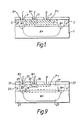
- a known collector-diffused isolation device or transistor is illustrated in Figure 1.
- An epitaxial layer 3 of p-type material is deposited upon a substrate.
- a collector area 5 is diffused or implanted through the epitaxial layer 3 and a base area 7 of the layer 3 is doped or implanted to become P+ type material.
- a collector contact 9 and an emitter contact 11 are provided by doping.
- the collector contact 9 and emitter contact 11 are both of N+ type material.
- the width of the base area 7 is controlled by the epitaxial layer 3 and the base diffusion, consequently it is difficult to fabricate the base area 7 with a narrow width. This leads to a problem with CDI transistors namely that of a low cut-off frequency (F T ) due to the shunt effect of a relatively large capacitance. (See Physics of Semiconductor Devices S.M. Sze p 158-9 (2nd Edition, Wiley)).
- CDI collector-diffused isolation
- a method for fabricating a collector diffused isolation device comprising a P type epitaxial layer upon a substrate with a diffused N+ type collector and a diffused N+ type emitter in a diffused P+ type base volume, the method being characterised in that at least a portion of the P type epitaxial layer is counter-doped to N type for the entire epitaxial depth to facilitate a more accurate definition of the base volume and to allow fabrication of a collector diffused isolation device having a reduced base volume width compared to conventional collector diffused isolation devices whilst selective counter doping preserves collector diffused isolation.
- a method for fabricating a collector diffused isolation device comprising an N type epitaxial layer upon a substrate with a diffused P+ type collector and a diffused P+ type emitter in a diffused N+ type base volume, the method being characterised in that at least a portion of the N type epitaxial layer is counter-doped to P type for the entire epitaxial depth to facilitate a more accurate definition of the base volume and to allow fabrication of a collector diffused isolation device having a reduced base volume width compared to conventional collector diffused isolation devices whilst selective counter doping preserves collector diffused isolation.
- an N+ type material slab 25 is formed, for example by gaseous diffusion or ion implantation.
- an epitaxial layer 23 of P type material is deposited on the P type substrate 21.
- an N type material well 27 is formed through the epitaxial layer 23 and extends into the slab 25 using standard VLSI masking techniques.
- This well 27 may be formed by gaseous diffusion or ion implantation.
- a collector volume 29 is doped to form an N+ type material enclosing the N type material well 27.
- a base area 32 of narrow width is deposited by diffusion or ion implantation, as illustrated in Figure 6.
- An oxide layer 37 is then formed on the surface of layer 23 by thermal oxidation.
- apertures are opened in the oxide layer 37 to allow subsequent contact to collector area 29, and base area 32.
- collector contact 33 and an emitter 35 each of N+ type material are then formed respectively in the collector volume 29 and base area 32 ( Figure 8).
- N-type material well 27 through the P-type epitaxial layer 23 that allows a base area 32 of narrow width to be formed.
- the effect of counter-doping of the epitaxial layer 23 is to form the N type material well 27.
- the N-type material well can be defined by a simple photolithographic technique thus retaining the simplicity of the collector diffused isolation (CDI) approach.
- CDI collector diffused isolation
- N-well CDI transistor is schematically illustrated in Figure 9. If a comparison is made to Figure 1, it will be seen that the collector (C)/base (B) junction area is significantly reduced by the introduction of an N-well 27. Futhermore, the N-well CDI transistor has a lower collector-base capacitance, higher sustaining voltage, a good early voltage and a better collector/base voltage.
Landscapes
- Bipolar Transistors (AREA)
Applications Claiming Priority (2)
| Application Number | Priority Date | Filing Date | Title |
|---|---|---|---|
| GB8915171 | 1989-07-01 | ||
| GB8915171A GB2234111B (en) | 1989-07-01 | 1989-07-01 | A method for fabrication of a collector-diffused isolation semiconductor device |
Publications (2)
| Publication Number | Publication Date |
|---|---|
| EP0407111A2 true EP0407111A2 (de) | 1991-01-09 |
| EP0407111A3 EP0407111A3 (en) | 1991-03-20 |
Family
ID=10659407
Family Applications (1)
| Application Number | Title | Priority Date | Filing Date |
|---|---|---|---|
| EP19900307177 Withdrawn EP0407111A3 (en) | 1989-07-01 | 1990-06-29 | A method for fabrication of a collector-diffused isolation semiconductor device |
Country Status (2)
| Country | Link |
|---|---|
| EP (1) | EP0407111A3 (de) |
| GB (1) | GB2234111B (de) |
Cited By (2)
| Publication number | Priority date | Publication date | Assignee | Title |
|---|---|---|---|---|
| EP0653760A3 (de) * | 1993-11-17 | 1995-11-22 | Samsung Electronics Co Ltd | Spannungserhöhungsschaltung. |
| DE10139515A1 (de) * | 2001-08-10 | 2003-03-06 | Infineon Technologies Ag | Transistor für eine Bandabstandsschaltung |
Families Citing this family (1)
| Publication number | Priority date | Publication date | Assignee | Title |
|---|---|---|---|---|
| KR0171128B1 (ko) * | 1995-04-21 | 1999-02-01 | 김우중 | 수직형 바이폴라 트랜지스터 |
Family Cites Families (5)
| Publication number | Priority date | Publication date | Assignee | Title |
|---|---|---|---|---|
| SE373984B (de) * | 1973-03-19 | 1975-02-17 | Ericsson Telefon Ab L M | |
| GB1557834A (en) * | 1976-11-27 | 1979-12-12 | Ferranti Ltd | Semiconductor devices and to circuit arrangements including such devices |
| JPS5978555A (ja) * | 1982-10-27 | 1984-05-07 | Toshiba Corp | 半導体装置 |
| CN1004456B (zh) * | 1985-04-19 | 1989-06-07 | 三洋电机株式会社 | 半导体器件及其制造方法 |
| EP0255882A3 (de) * | 1986-08-07 | 1990-05-30 | Siemens Aktiengesellschaft | npn-Bipolartransistor mit extrem flachen Emitter/Basis-Strukturen und Verfahren zu seiner Herstellung |
-
1989
- 1989-07-01 GB GB8915171A patent/GB2234111B/en not_active Expired - Lifetime
-
1990
- 1990-06-29 EP EP19900307177 patent/EP0407111A3/en not_active Withdrawn
Cited By (4)
| Publication number | Priority date | Publication date | Assignee | Title |
|---|---|---|---|---|
| EP0653760A3 (de) * | 1993-11-17 | 1995-11-22 | Samsung Electronics Co Ltd | Spannungserhöhungsschaltung. |
| DE10139515A1 (de) * | 2001-08-10 | 2003-03-06 | Infineon Technologies Ag | Transistor für eine Bandabstandsschaltung |
| DE10139515C2 (de) * | 2001-08-10 | 2003-07-31 | Infineon Technologies Ag | Bandabstandsschaltung |
| US6768139B2 (en) | 2001-08-10 | 2004-07-27 | Infineon Technologies Ag | Transistor configuration for a bandgap circuit |
Also Published As
| Publication number | Publication date |
|---|---|
| EP0407111A3 (en) | 1991-03-20 |
| GB2234111B (en) | 1992-12-02 |
| GB2234111A (en) | 1991-01-23 |
| GB8915171D0 (en) | 1989-08-23 |
Similar Documents
| Publication | Publication Date | Title |
|---|---|---|
| US6900519B2 (en) | Diffused extrinsic base and method for fabrication | |
| US4110126A (en) | NPN/PNP Fabrication process with improved alignment | |
| US4137109A (en) | Selective diffusion and etching method for isolation of integrated logic circuit | |
| JPH06112493A (ja) | 縦方向電流によるパワーmosトランジスタを製造するための方法およびこの方法により製造したトランジスタ | |
| JPH06151723A (ja) | モノリシック半導体素子のバイポーラトランジスタ構造、及び前記モノリシック半導体素子の製造方法 | |
| US5858828A (en) | Use of MEV implantation to form vertically modulated N+ buried layer in an NPN bipolar transistor | |
| JPS6322070B2 (de) | ||
| US4404738A (en) | Method of fabricating an I2 L element and a linear transistor on one chip | |
| US6897545B2 (en) | Lateral operation bipolar transistor and a corresponding fabrication process | |
| JPH07326773A (ja) | ダイオードおよびその製造方法 | |
| US4260431A (en) | Method of making Schottky barrier diode by ion implantation and impurity diffusion | |
| US20130207236A1 (en) | High-beta bipolar junction transistor and method of manufacture | |
| US4180827A (en) | NPN/PNP Fabrication process with improved alignment | |
| EP0476571A2 (de) | Halbleiterbauelement mit vertikalen Bipolartransistoren | |
| EP0407111A2 (de) | Verfahren zur Herstellung einer Diffusionskollektor-Isolationshalbleitervorrichtung | |
| JPH025564A (ja) | マルチコレクタ縦型pnpトランジスタ | |
| US6506656B2 (en) | Stepped collector implant and method for fabrication | |
| EP0627767B1 (de) | Verfahren zur Herstellung von JFET-Transistoren und Kondensatoren | |
| EP0375323A1 (de) | Ein vertikaler Hochleistungs-Bipolartransistor, Kompatibel mit einer hochwertigen ECL-Bipolar-Technologie und dessen Herstellungsverfahren | |
| US5001538A (en) | Bipolar sinker structure and process for forming same | |
| JPS61245573A (ja) | 半導体装置 | |
| US6624497B2 (en) | Semiconductor device with a reduced mask count buried layer | |
| US4692784A (en) | Dielectric insulation type semiconductor integrated circuit having low withstand voltage devices and high withstand voltage devices | |
| US5188971A (en) | Process for making a self-aligned bipolar sinker structure | |
| GB2143082A (en) | Bipolar lateral transistor |
Legal Events
| Date | Code | Title | Description |
|---|---|---|---|
| PUAI | Public reference made under article 153(3) epc to a published international application that has entered the european phase |
Free format text: ORIGINAL CODE: 0009012 |
|
| AK | Designated contracting states |
Kind code of ref document: A2 Designated state(s): DE FR IT NL |
|
| PUAL | Search report despatched |
Free format text: ORIGINAL CODE: 0009013 |
|
| RHK1 | Main classification (correction) |
Ipc: H01L 29/10 |
|
| AK | Designated contracting states |
Kind code of ref document: A3 Designated state(s): DE FR IT NL |
|
| 17P | Request for examination filed |
Effective date: 19910917 |
|
| RAP1 | Party data changed (applicant data changed or rights of an application transferred) |
Owner name: PLESSEY SEMICONDUCTORS LIMITED |
|
| 17Q | First examination report despatched |
Effective date: 19931008 |
|
| STAA | Information on the status of an ep patent application or granted ep patent |
Free format text: STATUS: THE APPLICATION IS DEEMED TO BE WITHDRAWN |
|
| 18D | Application deemed to be withdrawn |
Effective date: 19940219 |