EP0408253A2 - Wandler und deren Steuerung - Google Patents
Wandler und deren Steuerung Download PDFInfo
- Publication number
- EP0408253A2 EP0408253A2 EP90307361A EP90307361A EP0408253A2 EP 0408253 A2 EP0408253 A2 EP 0408253A2 EP 90307361 A EP90307361 A EP 90307361A EP 90307361 A EP90307361 A EP 90307361A EP 0408253 A2 EP0408253 A2 EP 0408253A2
- Authority
- EP
- European Patent Office
- Prior art keywords
- control
- voltage
- frequency
- series resonant
- resonant circuit
- Prior art date
- Legal status (The legal status is an assumption and is not a legal conclusion. Google has not performed a legal analysis and makes no representation as to the accuracy of the status listed.)
- Withdrawn
Links
Images





Classifications
-
- H—ELECTRICITY
- H02—GENERATION; CONVERSION OR DISTRIBUTION OF ELECTRIC POWER
- H02M—APPARATUS FOR CONVERSION BETWEEN AC AND AC, BETWEEN AC AND DC, OR BETWEEN DC AND DC, AND FOR USE WITH MAINS OR SIMILAR POWER SUPPLY SYSTEMS; CONVERSION OF DC OR AC INPUT POWER INTO SURGE OUTPUT POWER; CONTROL OR REGULATION THEREOF
- H02M3/00—Conversion of DC power input into DC power output
- H02M3/22—Conversion of DC power input into DC power output with intermediate conversion into AC
- H02M3/24—Conversion of DC power input into DC power output with intermediate conversion into AC by static converters
- H02M3/28—Conversion of DC power input into DC power output with intermediate conversion into AC by static converters using discharge tubes with control electrode or semiconductor devices with control electrode to produce the intermediate AC
- H02M3/325—Conversion of DC power input into DC power output with intermediate conversion into AC by static converters using discharge tubes with control electrode or semiconductor devices with control electrode to produce the intermediate AC using devices of a triode or a transistor type requiring continuous application of a control signal
- H02M3/335—Conversion of DC power input into DC power output with intermediate conversion into AC by static converters using discharge tubes with control electrode or semiconductor devices with control electrode to produce the intermediate AC using devices of a triode or a transistor type requiring continuous application of a control signal using semiconductor devices only
- H02M3/337—Conversion of DC power input into DC power output with intermediate conversion into AC by static converters using discharge tubes with control electrode or semiconductor devices with control electrode to produce the intermediate AC using devices of a triode or a transistor type requiring continuous application of a control signal using semiconductor devices only in push-pull configuration
- H02M3/3376—Conversion of DC power input into DC power output with intermediate conversion into AC by static converters using discharge tubes with control electrode or semiconductor devices with control electrode to produce the intermediate AC using devices of a triode or a transistor type requiring continuous application of a control signal using semiconductor devices only in push-pull configuration with automatic control of output voltage or current
-
- H—ELECTRICITY
- H02—GENERATION; CONVERSION OR DISTRIBUTION OF ELECTRIC POWER
- H02M—APPARATUS FOR CONVERSION BETWEEN AC AND AC, BETWEEN AC AND DC, OR BETWEEN DC AND DC, AND FOR USE WITH MAINS OR SIMILAR POWER SUPPLY SYSTEMS; CONVERSION OF DC OR AC INPUT POWER INTO SURGE OUTPUT POWER; CONTROL OR REGULATION THEREOF
- H02M7/00—Conversion of AC power input into DC power output; Conversion of DC power input into AC power output
-
- H—ELECTRICITY
- H02—GENERATION; CONVERSION OR DISTRIBUTION OF ELECTRIC POWER
- H02M—APPARATUS FOR CONVERSION BETWEEN AC AND AC, BETWEEN AC AND DC, OR BETWEEN DC AND DC, AND FOR USE WITH MAINS OR SIMILAR POWER SUPPLY SYSTEMS; CONVERSION OF DC OR AC INPUT POWER INTO SURGE OUTPUT POWER; CONTROL OR REGULATION THEREOF
- H02M7/00—Conversion of AC power input into DC power output; Conversion of DC power input into AC power output
- H02M7/42—Conversion of DC power input into AC power output without possibility of reversal
- H02M7/44—Conversion of DC power input into AC power output without possibility of reversal by static converters
- H02M7/48—Conversion of DC power input into AC power output without possibility of reversal by static converters using discharge tubes with control electrode or semiconductor devices with control electrode
- H02M7/53—Conversion of DC power input into AC power output without possibility of reversal by static converters using discharge tubes with control electrode or semiconductor devices with control electrode using devices of a triode or transistor type requiring continuous application of a control signal
- H02M7/537—Conversion of DC power input into AC power output without possibility of reversal by static converters using discharge tubes with control electrode or semiconductor devices with control electrode using devices of a triode or transistor type requiring continuous application of a control signal using semiconductor devices only, e.g. single switched pulse inverters
- H02M7/5387—Conversion of DC power input into AC power output without possibility of reversal by static converters using discharge tubes with control electrode or semiconductor devices with control electrode using devices of a triode or transistor type requiring continuous application of a control signal using semiconductor devices only, e.g. single switched pulse inverters in a bridge configuration
- H02M7/53871—Conversion of DC power input into AC power output without possibility of reversal by static converters using discharge tubes with control electrode or semiconductor devices with control electrode using devices of a triode or transistor type requiring continuous application of a control signal using semiconductor devices only, e.g. single switched pulse inverters in a bridge configuration with automatic control of output voltage or current
- H02M7/53878—Conversion of DC power input into AC power output without possibility of reversal by static converters using discharge tubes with control electrode or semiconductor devices with control electrode using devices of a triode or transistor type requiring continuous application of a control signal using semiconductor devices only, e.g. single switched pulse inverters in a bridge configuration with automatic control of output voltage or current by time shifting switching signals of one diagonal pair of the bridge with respect to the other diagonal pair
-
- Y—GENERAL TAGGING OF NEW TECHNOLOGICAL DEVELOPMENTS; GENERAL TAGGING OF CROSS-SECTIONAL TECHNOLOGIES SPANNING OVER SEVERAL SECTIONS OF THE IPC; TECHNICAL SUBJECTS COVERED BY FORMER USPC CROSS-REFERENCE ART COLLECTIONS [XRACs] AND DIGESTS
- Y02—TECHNOLOGIES OR APPLICATIONS FOR MITIGATION OR ADAPTATION AGAINST CLIMATE CHANGE
- Y02B—CLIMATE CHANGE MITIGATION TECHNOLOGIES RELATED TO BUILDINGS, e.g. HOUSING, HOUSE APPLIANCES OR RELATED END-USER APPLICATIONS
- Y02B70/00—Technologies for an efficient end-user side electric power management and consumption
- Y02B70/10—Technologies improving the efficiency by using switched-mode power supplies [SMPS], i.e. efficient power electronics conversion e.g. power factor correction or reduction of losses in power supplies or efficient standby modes
Definitions
- the present invention relates to converters such as include resonant inverters. This invention also relates to the control of an inverter, and to a DC to DC converter.
- Resonant inverters advantageously have low switching losses and low switching stresses.
- resonant operation is complex due to the fast dynamics of the high-frequency resonant tank circuit; and, hence, control is difficult.
- one known resonant inverter output load voltage or current control method is to vary the frequency of the rectangular wave signal supplied to the resonant circuit by the inverter via closed loop control.
- Commonly assigned U.S. Patent No. 4,541,041, issued on September 10, 1985 to J.N. Park and R.L. Steigerwald which is hereby incorporated by reference, discloses in part such a frequency control technique.
- the resonant nature of the circuit allows for control of output voltage or current through variation of the frequency at which the inverter's controllable switch means operate.
- Such a frequency control method has been found satisfactory under normal output load conditions for particular types of resonant inverters (i.e., heavy or medium load conditions for a series resonant inverter and light load conditions for a parallel resonant inverter).
- the drawback to frequency control is that it may be inadequate to maintain a desired output voltage or current under extended output load conditions (i.e., light or no load conditions for a series resonant inverter and heavy load conditions for a parallel resonant inverter).
- frequency control of a series resonant inverter will normally be adequate to maintain a desired output voltage during heavy or medium load conditions (i.e., low load resistance); that is, for heavy or medium load conditions, a series resonant circuit has a high quality factor Q and thus a good dynamic range of voltage or current change as frequency is varied.
- a series resonant circuit exhibits a low quality factor Q and thus only a small dynamic range of output voltage or current change can be achieved as a function of frequency.
- a resonant inverter control which provides an improved dynamic range of output voltage or current control is disclosed in U.S. Patent No. 4,672,528, issued June 9, 1987 to J.N. Park and R.L. Steigerwald and assigned to the assignee of the present invention.
- This patent which is hereby incorporated by reference, describes a resonant inverter which is controlled using either a frequency control mode or a phase shift control mode.
- output voltage is controlled by varying the frequency of the rectangular wave signal supplied to the resonant circuit within an operable range of the controllable switch means.
- Selecting means allows the control to operate in the phase shift control mode when the frequency of the rectangular wave signal is at an extremity of the operable range of the controllable switch means.
- each state trajectory corresponds to particular values of instantaneous resonant tank energy, output voltage, output current and switching frequency.
- One aspect of this invention seeks to provide a resonant inverter control which utilizes a combination of optimal control methods and phase modulation to maintain output load voltage substantially constant during all loading conditions.
- Another aspect of this invention seeks to provide a resonant inverter control which switches automatically between different control means to maintain a substantially constant output load voltage.
- An embodiment of the present invention exhibits an improved dynamic range of output load voltage control and/or maintains a desired output load voltage.
- a resonant inverter is controlled using a combination of optimal trajectory control and phase modulation.
- optimal control means are employed to continuously monitor resonant capacitor voltage, resonant inductor current, rectangular wave voltage applied to the resonant tank circuit and output load voltage, thereby determining the instantaneous "states" of the resonant inverter.
- a control law defined in terms of state plane analysis, enables maintenance of stable operation on state trajectories corresponding to particular values of the aforementioned state determinants. In this way, the improved control enables a time optimal response corresponding to a change in load conditions and, hence, a fast and efficient transition between state trajectories.
- a first control means When operating within the operable frequency range of the controllable switch means (i.e. below this maximum frequency and above the resonant frequency), a first control means provides frequency control signals which frequency modulate the rectangular wave voltage applied to the series resonant circuit so as to provide a constant output voltage and maintain stable operation.
- inverter control At an extremity of the operable frequency range of the controllable switch means, inverter control automatically switches to a second control means.
- the second control means calculates a phase modulation angle corresponding to the desired output voltage and generates a phase shift control signal representative thereof.
- a method for controlling output load voltage through a combination of optimal control methods and phase modulation.
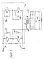
- a preferred resonant inverter control of the present invention will be described with reference to the dc-to-dc converter shown in Figure 1.
- An external source (not shown) provides input dc voltage V s to the converter at terminals 10 and 11.
- a full bridge inverter 12 Connected across terminals 10 and 11 is a full bridge inverter 12 having four switching devices that are capable of carrying reverse current and capable of being turned off by a switching signal.
- the switching devices are illustrated as bipolar junct-ion transistors (BJTs) S1, S2, S3 and S4. Each respective switching device has a diode D1, D2, D3 and D4 connected in inverse parallel therewith, respectively.
- the switching devices are turned on at zero current, and the inverse parallel diodes are commutated naturally. Hence, fast recovery diodes are not required.
- other switching devices with gate turn-off capability could be used instead of the BJTs, such as FETs each having an integral parasitic diode for carrying reverse current or monolithic Darlington power transistors.
- FETs field-effect transistors
- the full bridge inverter is illustrated for purposes of description only and that the control technique of the present invention is not limited to such an inverter.
- a series resonant tank circuit comprising an inductor 14, a capacitor 16, and the primary winding of an isolation transformer 18, is connected between junctions a and b.
- the secondary winding of transformer 18 is connected to the input of a full wave rectifier 20.
- the output of the rectifier is connected in parallel with a filter capacitor 22 and an output load (not shown) across which the converter output voltage V o is produced.
- a desired converter output load voltage V d may be maintained during heavy load and medium load conditions by frequency control of the rectangular wave voltage V ab .
- variation of frequency within the operable range OF would be insufficient to attain the desired output load voltage V d .
- the present invention therefore, employs a control technique for enhancing the dynamic range of converter output voltage control primarily needed under light load or no load conditions.
- the switches are controlled by a method of optimal trajectory control.
- This method is derived from optimal control theory and state plane analysis.
- the "control law" of the system is determined by the desired state of the system.
- An instantaneous state of the system is a function of resonant capacitor voltage, resonant inductor current, voltage applied to the resonant tank circuit and output load voltage.
- An instantaneous state corresponds to a specific state trajectory. The desired state trajectory, therefore, determines the control law of the system.
- Figure 3 illustrates a state plane diagram for the resonant inverter of Figure 1.
- switching cycle interval is defined as the time necessary to traverse a state trajectory.
- state trajectory 23 represents the desired resonant inverter operation and corresponds to a particular operating frequency and to specific values of the above-listed state determinants (i.e., resonant capacitor voltage, resonant inductor current, voltage applied to the resonant tank circuit, and output load voltage).
- Trajectory 23 comprises trajectory segments AB, BC, CD and DA corresponding to the conduction intervals of switching devices S1-S4 and diodes D1-D4. Each trajectory segment is a circular arc with a center and a radius determined by the state of the switching devices.
- trajectory segment AB having center (V s - V o , 0) represents the conduction interval of switching devices S1 and S4.
- trajectory segment BC having center (-V s - V O , 0) represents the conduction interval for diodes D2 and D3
- trajectory segment CD having center (-V S + V O , 0) represents the conduction interval for switching devices S2 and S3
- trajectory segment DA having center (V s + V o , 0) represents the conduction interval for diodes D1 and D4.
- the desired or optimal trajectory determines the control law of the system and, hence, the construction thereof.
- another parameter characterizing each trajectory segment is the trajectory radius R d measured either from center (V s + V o ,O) or center (-V s - V o ,O).
- a control circuit computes radius R d from continuous measurements of the state determinants (i.e., resonant capacitor voltage, resonant inductor current, voltage applied to the resonant tank circuit, and output load voltage). In this way, the control circuit maintains system operation corresponding to the desired state trajectory by alternately switching the pairs of diagonally opposed switching devices.
- a control signal V CONTROL generated by an outer control loop, to be described hereinafter, enables the system to respond by making a time optimal transition to another steady state trajectory.
- a resonant inverter control system constructed in accordance with the control law of equation (2) advantageously enables time optimal control of the switching devices when operating above resonance within the operable frequency range thereof.
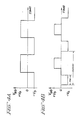
- optimal trajectory control according to Oruganti et al. is limited to bi-level or frequency modulation. That is, as shown in Figure 4A, the voltage applied to the resonant circuit is a rectangular wave signal having two levels: +V S and -V S .
- frequency of the rectangular wave signal may be varied to control output load voltage.
- the control range of output voltage is limited as the frequency increases to the maximum operating frequency of the switching devices.
- the present invention modifies and improves the above-described optimal trajectory control system to provide a new resonant control which yields a significantly increased range of controlled output load voltages under all loading conditions.
- the present invention combines optimal trajectory control with phase modulation.
- phase modulated signal takes the general tri-level form illustrated in Figure 4B, where pulse width pw varies proportionately as the phase modulation angle ⁇ .
- Figure 5 is a graph of the magnitude of fundamental harmonic F1 versus phase modulation angle ⁇ . As shown, for a 50% duty cycle (i.e., ⁇ - 0), the fundamental harmonic F1 is at its maximum value 4 ⁇ V s . As ⁇ increases, the amplitude of the fundamental harmonic decreases. Therefore, phase modulation can be used according to the present invention to decrease the amplitude of the fundamental harmonic of the voltage applied to the series resonant inverter. As a result, and as is evident from Figure 2, a broader range of controlled output load voltage may be obtained under all loading conditions by decreasing the effective voltage applied to the series resonant circuit.
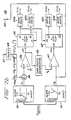
- FIG. 6 is a block diagram illustrating a resonant inverter control system employing the series resonant inverter control of the present invention.
- a commanded output voltage V REF is compared to output voltage V o by a summer 24.
- the resulting error signal V ERR is inputted to a proportional plus integral (PI) compensator 26 which generates control signal V CONTROL .
- Control signal V CONTROL is provided to series resonant inverter control 28 which drives inverter 12.
- Control signals proportional to the aforementioned state determinants are also inputted to series resonant inverter control 28. These signals are represented as: k1i L , k3v c , k3V o , and k3V s , where k1 and k3 are constant scale factors to be described hereinafter.
- FIGS 7a and 7b connected at points 27 and 29, respectively, illustrate the preferred embodiment of the improved resonant inverter control 28 of the present invention.
- the state trajectory of the present invention (not shown), therefore, is a modification of that of Figure 3 to account for the differences in a switching cycle interval resulting from the application of phase modulation to be described hereinafter.
- control circuit involves the use of sensing devices to detect instantaneous values of state determinants v c , i L , V s and V o . Since these sensing devices involve scaling to produce signals proportional to the respective state determinants, the following description, therefore, includes the aforementioned exemplary scale factors represented as constants k1 and k3.
- control signal k1i L which is proportional to resonant inductor current, is derived from a suitable current sensor 19.
- Typical current sensors are well known in the art and may comprise, as examples: Hall effect current sensors, current sensing resistors, or current sensing transformers.
- control signal k1i L is applied to a comparator 30.
- the output signal F of comparator 30 is either +1 or -1, depending upon the sign of inductor current i L .
- the signal F is inputted to multipliers 32 and 34, the value of F being the multiplicative factor thereof.
- the control signal k1i L is also applied to a multiplier 36 which performs a squaring operation to produce the signal k2(Z o i L ) 2, where Z o ⁇ L/C , a constant, is the characteristic impedance of the series resonant circuit, and k2 is also a constant.
- Control signal k3V s which is proportional to the applied source voltage, is supplied by a source voltage sensor 21 to a multiplier 31 which multiplies control signal k3v s by cos ⁇ , where ⁇ is the aforementioned phase modulation angle value.
- Suitable voltage sensors are well known in the art and may comprise, for example, a voltage dividing network of resistors.
- Signal k3V s cos ⁇ is applied to multiplier 32 and is thereby multiplied by signal F.
- Control signal k3V o which is proportional to the output load voltage, is produced by a voltage sensor 23 and applied to multiplier 34 to yield a signal Fk3V o .
- a summer 40 adds the signal Fk3V o to still another sensed control signal k3v c , which is sensed by a voltage sensor 25 and is proportional to the voltage across the resonant capacitor.
- the resulting signal k3(v c - FV o ) is added to the aforementioned signal Fk3V s cos ⁇ by summer 42 to yield the signal k3(v c - FV o - FV s cos ⁇ ).
- the latter signal is inputted to a multiplier 44 which performs a squaring operation.
- the resulting squared signal k2(v c - FV o - FV s cos ⁇ )2 is added to the hereinabove derived signal k2(Z o i L )2 by a summer 46 and, as shown in Figure 7b, is then inputted to gain amplifier 48 having the transfer function -k4/k2 where k4 is a constant.
- the output of amplifier 48 is a signal -k4[(v c - FV o - FV s cos ⁇ )2 + (Z o i L )2],which is hereinafter referred to as the optimal control signal.
- Control signal V CONTROL is provided to a frequency modulation controller 50 and a phase modulation controller 52.
- the transfer function of frequency modulation controller 50 is shown in Figure 7b and may be represented mathematically as: where V F is the output voltage of frequency modulation controller 50, V T is a threshold voltage representing operation at an extremity of the operable frequency range for the controllable switch means, and C1 is a constant.
- Voltage V F is added in a summer 54 to the output signal of gain amplifier 48, and the result is inputted to the non-inverting input of a comparator 56.
- the output signal from comparator 56 is supplied to a sawtooth generator 58.
- phase modulation Controller 52 is also shown in Figure 7b and may be represented mathematically as: where V ⁇ is the output voltage from phase modulation controller 52, ⁇ being proportional to phase modulation angle ⁇ , and C2 is a constant. Voltage V ⁇ is inputted to the inverting input of a comparator 60. The output signal V G of sawtooth generator 58 is supplied to the noninverting input of comparator 60. Voltage V ⁇ is also supplied to multiplier 31 for which cos ⁇ is the multiplicative factor.
- the output signals CP1 and CP2 from comparators 56 and 60, respectively, provide the clock pulses for D-type (delay) flip-flops 62 and 64, respectively.
- D flip-flop 62 is a divide-by-two flip-flop; that is, the output frequency is one-half that of the clock frequency.
- the output signals from the D flip-flops control the base drive circuitry 65a-65d for the respective switching devices S1-S4. Suitable base drive circuitry is well-known in the art.
- the sawtooth generator produces a voltage ramp signal V G operating at twice the frequency of gate drive circuitry 65a-65d.
- the voltage ramp signal V G resets to zero each time the output signal at Q1 of D flip-flop 62 transitions from logic level 0 to 1 or 1 to 0.
- the output ramp voltage of sawtooth generator 58 is compared with voltage V ⁇ by comparator 60 which provides clock pulses for D flip-flop 64.
- D flip-flop 64 For a positive edge triggered D flip-flop 64, for example, when the output signal of comparator 60 transitions from a low logic level to a high logic level, the signal at output Q2 of D-flip-flop 64 latches to the same value as the signal at output Q1 of D flip-flop 62.
- the output voltage V F of frequency modulation controller 50 is C1V CONTROL
- there is frequency modulation That is, the output voltage C1V CONTROL of frequency modulation controller 50 is added to the output signal of summing amplifier 48 and applied to the non-inverting input of comparator 56.
- the output signal CP1 of comparator 56 provides clock pulses to D flip-flop 62 to toggle its state and, as stated above, also drives sawtooth generator 58.
- D flip-flop 64 is toggled almost simultaneously with D flip-flop 62. In this way, for V CONTROL ⁇ V T , frequency modulation using optimal control is achieved when operating within the operable frequency range of the switching devices.
- the output voltage V F of frequency modulation controller 50 is C1V T , a constant, so that the switching frequency of switching devices S1, S2, S3 and S4 is fixed at an extremity of the operable frequency range thereof.
- the output voltage V ⁇ of phase modulation controller 52 is C2(V CONTROL - V T ).
- This voltage V ⁇ is compared with the output signal VG of sawtooth generator 58 by comparator 60.
- the clock pulses CP2 from comparator 60 to D flip-flop 64 are delayed by an amount of time proportional to phase modulation angle ⁇ .
- Voltage V ⁇ also enables multiplier 31 to multiply source voltage V S by cos ⁇ .
- phase modulation is employed to produce the tri-level voltage waveform shown in Figure 4B for controlling the series resonant inverter.
- Figures 8a-8i are waveforms that illustrate in detail the operation of the new resonant inverter control for a specific case of V CONTROL > V T .
- the output signal CP1 of comparator 56 has a constant pulse width and is represented by the signal of Figure 8a.
- the output signals at Q1 and Q1 are illustrated in Figures 8b and 8c, respectively.
- Voltage ramp signal V G from sawtooth generator 58, which is reset each time the output signals from D flip-flop 62 change state is shown in Figure 8d.
- Voltage V ⁇ which determines the phase modulation angle ⁇ , is illustrated as a voltage between 0 and 10V in Figure 8e.
- phase modulation angle ⁇ ⁇ 4 radians for this example.
Landscapes
- Engineering & Computer Science (AREA)
- Power Engineering (AREA)
- Inverter Devices (AREA)
- Dc-Dc Converters (AREA)
- Feedback Control In General (AREA)
Applications Claiming Priority (2)
| Application Number | Priority Date | Filing Date | Title |
|---|---|---|---|
| US379461 | 1989-07-13 | ||
| US07/379,461 US4951185A (en) | 1989-07-13 | 1989-07-13 | Resonant inverter employing frequency and phase modulation using optimal trajectory control |
Publications (2)
| Publication Number | Publication Date |
|---|---|
| EP0408253A2 true EP0408253A2 (de) | 1991-01-16 |
| EP0408253A3 EP0408253A3 (en) | 1991-03-27 |
Family
ID=23497361
Family Applications (1)
| Application Number | Title | Priority Date | Filing Date |
|---|---|---|---|
| EP19900307361 Withdrawn EP0408253A3 (en) | 1989-07-13 | 1990-07-05 | Converters and the control thereof |
Country Status (5)
| Country | Link |
|---|---|
| US (1) | US4951185A (de) |
| EP (1) | EP0408253A3 (de) |
| JP (2) | JP3311743B2 (de) |
| KR (1) | KR910003901A (de) |
| CA (1) | CA2012811A1 (de) |
Cited By (6)
| Publication number | Priority date | Publication date | Assignee | Title |
|---|---|---|---|---|
| EP0784374A3 (de) * | 1996-01-11 | 1998-07-22 | The Miller Group, Ltd. | Leistungsversorgung |
| US6115273A (en) * | 1998-07-09 | 2000-09-05 | Illinois Tool Works Inc. | Power converter with low loss switching |
| EP1078378A4 (de) * | 1998-05-22 | 2004-04-21 | Minebea Co Ltd | Variabler induktivität |
| US6865096B1 (en) | 1998-07-09 | 2005-03-08 | Illinois Tool Works Inc. | Power convertor with low loss switching |
| WO2011006861A3 (de) * | 2009-07-14 | 2011-05-05 | Siemens Aktiengesellschaft | Störungsarme spannungsversorgung |
| EP2720365A3 (de) * | 2012-10-12 | 2017-09-27 | Fuji Electric Co., Ltd. | Bidirektionaler Gleichstromwandler |
Families Citing this family (28)
| Publication number | Priority date | Publication date | Assignee | Title |
|---|---|---|---|---|
| JP2588786B2 (ja) * | 1990-02-26 | 1997-03-12 | オリジン電気株式会社 | X線電源装置 |
| US5452197A (en) * | 1993-02-04 | 1995-09-19 | Vanner Weldon, Inc. | Static DC to AC power converter including separate high and low power converters |
| ATE134087T1 (de) * | 1993-03-22 | 1996-02-15 | Siemens Ag | Verfahren und vorrichtung zur arbeitspunktregelung eines reihenschwingkreis- wechselrichters |
| US5534766A (en) * | 1994-04-01 | 1996-07-09 | General Electric Company | Fuzzy logic power supply controller |
| DE19724931A1 (de) * | 1997-06-12 | 1998-12-17 | Philips Patentverwaltung | Leistungsversorgungseinheit mit einem pulsdauermodulierten Wechselrichter, insbesondere für einen Röntgengenerator |
| US20080068132A1 (en) * | 2006-05-16 | 2008-03-20 | Georges Kayanakis | Contactless radiofrequency device featuring several antennas and related antenna selection circuit |
| WO2007141349A1 (es) * | 2006-06-05 | 2007-12-13 | Suinsa Medical Systems S.A. | Etapa inversora electrónica de potencia |
| JP2010506559A (ja) * | 2006-10-13 | 2010-02-25 | コーニンクレッカ フィリップス エレクトロニクス エヌ ヴィ | 二次回路に給電する一次共振インバーター回路 |
| JP5495675B2 (ja) * | 2009-08-26 | 2014-05-21 | 三菱電機株式会社 | 発光ダイオード点灯装置及び照明器具及び照明システム |
| US8390373B2 (en) * | 2010-06-08 | 2013-03-05 | MUSIC Group IP Ltd. | Ultra-high efficiency switching power inverter and power amplifier |
| CN103078510B (zh) * | 2011-10-25 | 2015-11-25 | 通用电气公司 | 谐振电源、磁共振成像系统及控制方法 |
| CN103076580B (zh) * | 2011-10-25 | 2016-02-03 | 通用电气公司 | 梯度放大器、逆变器控制器、磁共振成像系统及控制方法 |
| CN103078515A (zh) | 2011-10-25 | 2013-05-01 | 通用电气公司 | 谐振电源、变换器控制器、磁共振成像系统及控制方法 |
| CN103105565B (zh) * | 2011-11-09 | 2015-07-08 | 丁一舟 | 采用调频移相的串联谐振耐压局放试验方法 |
| EP2811638B1 (de) | 2012-02-03 | 2017-12-20 | Fuji Electric Co., Ltd. | Steuerungsvorrichtung für gleichspannungsresonanzwandler |
| JP5906418B2 (ja) * | 2012-06-15 | 2016-04-20 | パナソニックIpマネジメント株式会社 | 電力変換装置 |
| WO2015004989A1 (ja) | 2013-07-11 | 2015-01-15 | 富士電機株式会社 | 双方向dc/dcコンバータ |
| US9509225B2 (en) * | 2014-09-16 | 2016-11-29 | Continental Automotive Systems, Inc. | Efficient LLC resonant converter having variable frequency control and fixed frequency phase-shift PWM |
| JP6141908B2 (ja) * | 2015-05-18 | 2017-06-07 | 東芝デベロップメントエンジニアリング株式会社 | 電流共振型dc−dcコンバータ |
| JP6573502B2 (ja) * | 2015-08-07 | 2019-09-11 | 新電元工業株式会社 | Dc−dcコンバータ |
| JP6526546B2 (ja) * | 2015-11-26 | 2019-06-05 | 株式会社日立情報通信エンジニアリング | 共振形電源装置 |
| JP2019047539A (ja) * | 2017-08-29 | 2019-03-22 | 新電元工業株式会社 | スイッチング電源 |
| US10917017B1 (en) | 2019-12-17 | 2021-02-09 | Ge Precision Healthcare | System and method to control a resonant power converter |
| JP7541298B2 (ja) | 2021-01-13 | 2024-08-28 | 富士電機株式会社 | 電力変換装置、電力変換装置の制御装置、および、電力変換制御方法 |
| US20240235403A1 (en) * | 2021-06-30 | 2024-07-11 | Mitsubishi Electric Corporation | Power conversion device |
| CN116633141A (zh) * | 2022-02-14 | 2023-08-22 | 台达电子企业管理(上海)有限公司 | 谐振变换器的参数估计方法、谐振变换器的控制方法与谐振变换器 |
| FR3152681A1 (fr) * | 2023-09-03 | 2025-03-07 | Valeo Eautomotive Germany Gmbh | Convertisseur continu-continu, engin de mobilite comportant un tel convertisseur continu-continu, procede de commande d’un convertisseur continu-continu et programme d’ordinateur correspondant |
| CN119813717A (zh) * | 2024-12-23 | 2025-04-11 | 杭州电子科技大学 | 适用于对称型cllc谐振变换器的快速切载控制方法 |
Family Cites Families (4)
| Publication number | Priority date | Publication date | Assignee | Title |
|---|---|---|---|---|
| US4477868A (en) * | 1982-09-30 | 1984-10-16 | General Electric Company | High frequency series resonant dc-dc converter |
| US4541041A (en) * | 1983-08-22 | 1985-09-10 | General Electric Company | Full load to no-load control for a voltage fed resonant inverter |
| US4672528A (en) * | 1986-05-27 | 1987-06-09 | General Electric Company | Resonant inverter with improved control |
| US4670832A (en) * | 1986-06-12 | 1987-06-02 | General Electric Company | Resonant inverter having improved control at enablement |
-
1989
- 1989-07-13 US US07/379,461 patent/US4951185A/en not_active Ceased
-
1990
- 1990-03-22 CA CA002012811A patent/CA2012811A1/en not_active Abandoned
- 1990-07-05 EP EP19900307361 patent/EP0408253A3/en not_active Withdrawn
- 1990-07-12 KR KR1019900010541A patent/KR910003901A/ko not_active Withdrawn
- 1990-07-13 JP JP18442790A patent/JP3311743B2/ja not_active Expired - Fee Related
-
2002
- 2002-03-04 JP JP2002057039A patent/JP3392128B2/ja not_active Expired - Fee Related
Cited By (10)
| Publication number | Priority date | Publication date | Assignee | Title |
|---|---|---|---|---|
| EP0784374A3 (de) * | 1996-01-11 | 1998-07-22 | The Miller Group, Ltd. | Leistungsversorgung |
| EP1078378A4 (de) * | 1998-05-22 | 2004-04-21 | Minebea Co Ltd | Variabler induktivität |
| US6115273A (en) * | 1998-07-09 | 2000-09-05 | Illinois Tool Works Inc. | Power converter with low loss switching |
| US6426888B2 (en) | 1998-07-09 | 2002-07-30 | Illinois Tool Works Inc. | Power convertor with low loss switching |
| US6625046B2 (en) | 1998-07-09 | 2003-09-23 | Illinois Tool Works Inc. | Power convertor with low loss switching |
| US6865096B1 (en) | 1998-07-09 | 2005-03-08 | Illinois Tool Works Inc. | Power convertor with low loss switching |
| US7336512B2 (en) | 1998-07-09 | 2008-02-26 | Illinois Tool Works Inc. | Power convertor with low loss switching |
| US7778056B2 (en) | 1998-07-09 | 2010-08-17 | Geissler Steven J | Power converter with low loss switching |
| WO2011006861A3 (de) * | 2009-07-14 | 2011-05-05 | Siemens Aktiengesellschaft | Störungsarme spannungsversorgung |
| EP2720365A3 (de) * | 2012-10-12 | 2017-09-27 | Fuji Electric Co., Ltd. | Bidirektionaler Gleichstromwandler |
Also Published As
| Publication number | Publication date |
|---|---|
| JP3311743B2 (ja) | 2002-08-05 |
| US4951185A (en) | 1990-08-21 |
| JP2002262569A (ja) | 2002-09-13 |
| KR910003901A (ko) | 1991-02-28 |
| JP3392128B2 (ja) | 2003-03-31 |
| CA2012811A1 (en) | 1991-01-13 |
| EP0408253A3 (en) | 1991-03-27 |
| JPH03128672A (ja) | 1991-05-31 |
Similar Documents
| Publication | Publication Date | Title |
|---|---|---|
| US4951185A (en) | Resonant inverter employing frequency and phase modulation using optimal trajectory control | |
| USRE33866E (en) | Resonant inverter employing frequency and phase modulation using optimal trajectory control | |
| US5519306A (en) | Constant voltage circuit and a stabilized power supply unit | |
| CN1405963B (zh) | 改进开关电源半桥转换器的稳定性和动态响应的装置和方法 | |
| US6351401B1 (en) | Series resonant converter comprising a control circuit | |
| US5051880A (en) | Mixed mode regulation controller for a resonant power converter | |
| EP0107313B1 (de) | Stromgesteuerte-Resonanzenergiequelle | |
| US4244015A (en) | Pulse width modulated inverter | |
| US4649467A (en) | High efficiency MOSFET sine wave generator | |
| WO1990002441A1 (en) | Regulated transformer rectifier unit | |
| US4317165A (en) | Inverter having improved efficiency and regulation | |
| JPH0126273B2 (de) | ||
| JPH03117366A (ja) | 直列共振インバータに対する負荷補償利得制御方式 | |
| GB2114780A (en) | Current control pulse width modulated inverter machine drive system | |
| RU2216845C2 (ru) | Способ управления обратимым преобразователем энергии переменного тока в энергию постоянного тока | |
| JP3183559B2 (ja) | 交流電子負荷装置 | |
| EP0081302B1 (de) | Reihenresonanz Gleichspannungswandler mit integrierendem Rückführungskreis | |
| JP2976603B2 (ja) | 直列共振コンバータ制御回路 | |
| JP2604302Y2 (ja) | 共振形dc−dcコンバータ | |
| JP2738354B2 (ja) | 広入力圧電トランスコンバータ | |
| GB1594400A (en) | Symmetry control system for a converter | |
| JP3332046B2 (ja) | 放電灯回路装置 | |
| RU1815776C (ru) | Широтно-импульсный N-фазный инвертор | |
| JPH0746072Y2 (ja) | インバ−タの出力電圧補償回路 | |
| JP2913682B2 (ja) | 周波数同調回路 |
Legal Events
| Date | Code | Title | Description |
|---|---|---|---|
| PUAI | Public reference made under article 153(3) epc to a published international application that has entered the european phase |
Free format text: ORIGINAL CODE: 0009012 |
|
| AK | Designated contracting states |
Kind code of ref document: A2 Designated state(s): DE FR GB NL |
|
| PUAL | Search report despatched |
Free format text: ORIGINAL CODE: 0009013 |
|
| AK | Designated contracting states |
Kind code of ref document: A3 Designated state(s): DE FR GB NL |
|
| 17P | Request for examination filed |
Effective date: 19910905 |
|
| 17Q | First examination report despatched |
Effective date: 19930701 |
|
| STAA | Information on the status of an ep patent application or granted ep patent |
Free format text: STATUS: THE APPLICATION IS DEEMED TO BE WITHDRAWN |
|
| 18D | Application deemed to be withdrawn |
Effective date: 19931112 |